TenGEMAC IP Core Data Sheet

Core Facts |
|
|
Provided with Core |
|
|
Documentation |
User Guide, Design Guide |
|
Design File Formats |
Encrypted hdl File |
|
Instantiation Templates |
VHDL |
|
Reference Designs & Application Notes |
QuartusII Project, See Reference Design Manual |
|
Additional Items |
Demo on Arria10 GX and Arria10 SoC development board |
|
Support |
|
|
Support Provided by Design Gateway Co., Ltd. |
|
Design Gateway Co.,Ltd
E-mail: ip-sales@design-gateway.com
URL: design-gateway.com
Features
· 10 Gbps Ethernet
· 10G PHY interface: 64-bit XGMII interface at 156.25 MHz
· Same clock domain for transmit and receive XGMII interface
· User interface: 64-bit Avalon-ST interface, directly connect to TOE10G IP or UDP10G IP
· Low transmit and receive latencies (3 clock cycles for transmit side, 7 clock cycles fo receive side)
· FCS inserting (CRC-32) to the transmit packet
· FCS checking (CRC-32) for the received packet
· Not append the zero padding in the transmit packet
· Not remove the zero padding from the received packet
· Support the 1st byte of Received XGMII data on byte0 (bit[7:0]) or byte4 (bit[39:32])
Table 1: Example Implementation Statistics
|
Family |
Example Device |
Fmax (MHz) |
ALMs |
Registers1 |
Pin2 |
Block Memory bit3 |
Design Tools |
|
Cyclone10 GX |
10CX220YF780E5G |
156.25 |
1,346 |
1,216 |
- |
- |
QuartusII 18.0 |
|
Arria10 SX |
10AS066N3F40E2SGE2 |
156.25 |
1,360 |
1,259 |
- |
- |
QuartusII 16.0 |
|
Arria10 GX |
10AX115S2F45I2SG |
156.25 |
1,362 |
1,256 |
- |
- |
QuartusII 16.0 |
Notes:
1) Actual logic resource dependent on percentage of unrelated logic
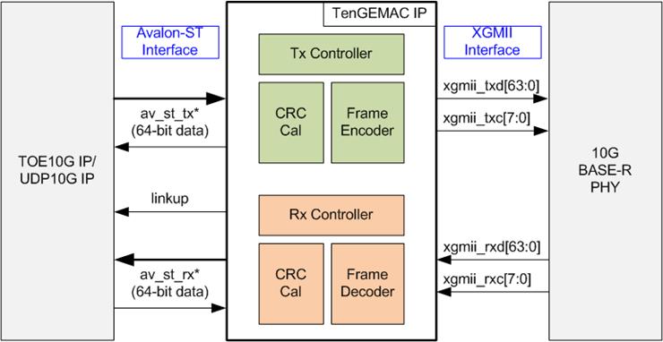
Figure 1: TenGEMAC IP Block Diagram
Applications
By using DG Network IP suite (TOE10G IP/UDP10G IP and TenGEMACIP), the system implemented on FPGA can transfer Ethernet packet via 10Gb Ethernet following TCP/IP protocol or UDP/IP protocol with good performance, low data latency, and small resource utilization. It is the solution to implement Ethernet streaming and monitoring system without CPU and external memory usage.
General Description
On the other hand, the received packet from XGMII interface (10G BASE-R PHY) is verified by TenGEMAC IP. The preamble, SFD, and FCS are removed from the received packet before forwarding to Avalon-ST interface. If the FCS is not correct, the IP asserts the error signal to Avalon-ST interface.
Data input stream of one packet on Avalon-ST interface must be transferred without pausing because TenGEMAC IP does not include Tx buffer to pause data transmission to 10G Ethernet PHY (BASE-R). Similarly, the received packet from 10G Ethernet PHY is forwarded to Avalon-ST interface continuously because there is no internal buffer of receive path in TenGEMAC IP.
TenGEMAC IP does not support zero padding function, so the user logic on Avalon-ST interface must append the padding by itself for the small packet which is less than 60 byte size. TenGEMAC IP supports to receive the packet from XGMII interface when the 1st byte is placed on byte0 (xgmii_rxd[7:0]) and byte 4 (xgmii_rxd[39:32]) only. Otherwise, the received packet is ignored.
Functional Description
TenGEMAC IP is designed to support data transmission in both directions at the same time. The logic to transmit data and receive data are run independently.
Transmit Block
· CRC Cal
This module is designed to calculate 32 bit CRC from 64-bit data, input from Avalon-ST interface. The polynomial of CRC-32 to create FCS following IEEE802.3 standard is shown as follows.
P(X) = X32 + X26 + X23 + X22 + X16 + X12 + X11 + X10 + X8 + X7 + X5 + X4 + X2 + X1 + 1
FCS is appended to the packet as the footer after finishing forwarding all data.
· Frame Encoder
This module inserts the header and the footer to the transmit packet from Avalon-ST interface. 7-byte preamble and 1-byte SFD (Start of frame delimiter) are appended as the header of the packet while 4-byte FCS and 1-byte EFD (End of frame delimiter) are appended as the footer of the packet. After finishing one frame, 12-Idle cycle is inserted to be IFG (interframe gap) between two packets.
· Tx Controller
The controller monitors the control signals on Avalon-ST interface. When the new frame is found, it will assert the control signal to the Frame encoder for inserting the header and the footer into the frame. After that, the controller de-asserts ready signal on Avalon-ST interface for 3 clock cycles to complete FCS, EFD and interframe gap insertion process.
Receive Block
· CRC Cal
This module is the same module as CRC Cal in Transmit Block. The FCS output from this module is applied to verify the received packet. The error will be asserted on Rx Avalon-ST interface if the FCS in the received packet is not correct.
· Frame Decoder
The data and control signals from XGMII interface are decoded by this module to check link up status, start of frame, and end of frame. The data type output from the decoder is forwarded to Rx controller to validate the data sequence in the packet. The received packet which removes the header and the footer is rearranged to align the 1st byte data of the packet on byte7 only. Therefore, the 1st byte data on Avalon-ST stream interface is always on av_st_rx_data[63:56].
· Rx Controller
The controller checks SFD and FCS in the received packet. The controller asserts the data valid to Avalon-ST interface when the packet header is correct. The error is asserted by the controller when the FCS of the packet is not correct.
TOE10G IP/UDP10G IP
TOE10G IP implements TCP/IP stack and the offload engine while UDP10G IP implements UDP/IP stack and the offload engine. More details of the IP are described in the datasheet.
https://dgway.com/products/IP/TOE10G-IP/dg_toe10gip_data_sheet_intel_en.pdf
https://dgway.com/products/IP/UDP10G-IP/dg_udp10gip_data_sheet_intel_en.pdf
10 Gb BASE-R PHY
The 10GBASE-R PHY Intel FPGA IP core allows connectivity directly with any XFP or SFP+ optical module. The PHY IP core can be used with either Intel FPGA IP for 10G Ethernet MAC or with a custom EMAC via a 64-bit XGMII interface running at 156.25 Mbps. This PHY IP core is made available as part of the transceiver functionality of the Intel FPGAs. For more details, please download the IP datasheet from the following link.
Core I/O Signals
Descriptions of all signal I/Os are provided in Table 2.
Table 2: Core I/O Signals
|
Signal |
Dir |
Description |
|
RstB |
In |
Reset IP core. Active Low. |
|
Clk |
In |
156.25 MHz fixed clock frequency input, synchronous to XGMII interface. |
|
IPVersion[31:0] |
Out |
IP version number |
|
Linkup |
Out |
Asserted to �1� when Rx XGMII sends Idle code (PHY initialization is finished). |
|
Avalon-ST Interface |
||
|
av_st_tx_data[63:0] |
In |
Transmitted data to Avalon-ST interface. Valid when av_st_tx_valid is asserted to �1�. |
|
av_st_tx_empty[2:0] |
In |
Specify the number of bytes which are unused of the final av_st_tx_data in the frame. The signal is valid when av_st_tx_valid and av_st_tx_endofpacket are asserted to �1�. |
|
av_st_tx_valid |
In |
Valid signal of transmitted data. Assert to �1� when av_st_tx_data is valid. |
|
av_st_tx_endofpacket |
In |
Assert to �1� to indicate the final word in the frame. Valid when av_st_tx_valid is asserted to �1�. |
|
av_st_tx_ready |
Out |
Handshaking signal. Asserted to �1� when av_st_tx_data has been accepted. This signal is not de-asserted to �0� when the packet is transmitting. |
|
av_st_rx_data[63:0] |
Out |
Received data. Valid when av_st_rx_valid is asserted to �1�. |
|
av_st_rx_empty[2:0] |
Out |
Specify the number of bytes which are unused of the final av_st_rx_data in the frame. The signal is valid when av_st_rx_valid and av_st_rx_endofpacket are asserted to �1�. |
|
av_st_rx_valid |
Out |
Received data valid signal. Asserted to �1� when av_st_rx_data/empty are valid. |
|
av_st_rx_endofpacket |
Out |
Asserted to �1� to indicate the final word in the frame. Valid when av_st_rx_valid is asserted to �1�. |
|
av_st_rxstatus_error |
Out |
Asserted at the end of the frame to indicate that the frame has an error. �0�: normal packet, �1�: error packet. Valid when av_st_rx_valid and av_st_rx_endofpacket are asserted to �1�. |
|
XGMII Interface |
||
|
xgmii_txd[63:0] |
Out |
Transmitted data to PHY |
|
xgmii_txc[7:0] |
Out |
Transmitted control to PHY |
|
xgmii_rxd[63:0] |
In |
Received data from PHY |
|
xgmii_rxc[7:0] |
In |
Received control from PHY |
Timing Diagram
IP Initialization
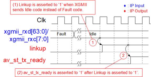
Figure 2: Linkup status
After finishing reset sequence, the IP monitors the received data from XGMII interface. When PHY is not ready, Fault code is returned from XGMII interface.
(1) After PHY finishes the initialization, XGMII sends Idle code instead of Fault code. After that, the IP changes linkup to �1�.
(2) Next, av_st_tx_ready is asserted to �1� to start packet transferring between Avalon-ST interface and XGMII interface.
Transmit interface
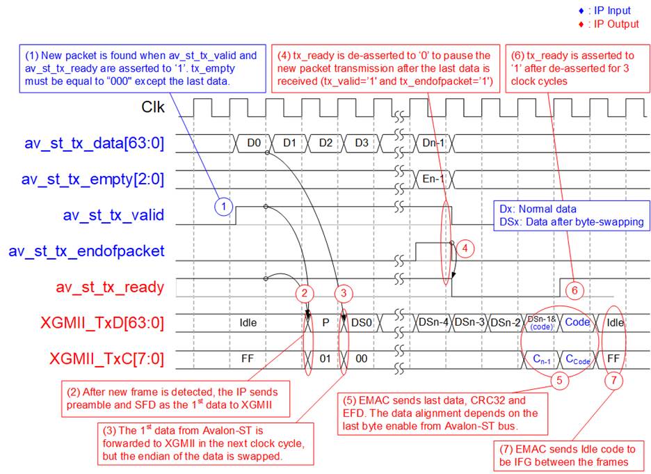
Figure 3: Transmit packet timing diagram
The example to send the data stream from Avalon-ST to XGMII is shown in Figure 3.
(1) The new packet is found when av_st_tx_valid is asserted to �1� with the IP ready status (av_st_tx_ready=�1�). All 64-byte data from Avalon-ST must be valid during packet transmission, except the last data. The number of unused bytes of the last data can be monitored by av_st_tx_empty signal.
(2) The IP starts the operation to calculate FCS (CRC-32) and appends 7-byte preamble and SFD to the packet as the 1st data.
(3) The IP forwards the 1st data from Avalon-ST to XGMII in the 2nd clock, but the endian is swapped. More details of byte-swapping are shown in Figure 4. TxC value during data forwarding is always equal to 0x00, except the last data which depends on tx_empty input at the end of frame.
(4) After the last data is found (detected by tx_valid=�1� and tx_endofpacket=�1�), the IP ready (av_st_tx_ready) is de-asserted to �0� for 3 clock cycles. During the gap size, the IP inserts 4-byte FCS, EFD, and 12-byte Idle for IFG. The gap size is also applied to compensate the time usage for inserting 8-byte header (7-byte preamble and SFD).
(5) The last data from Avalon-ST is forwarded to XGMII. If the last data is not aligned to 8, the IP will append the footer (4-byte FCS, EFD,and 12-byte Idle) to the remaining byte. The remaining footer is transmitted to XGMII in the next clock.
(6) The IP asserts tx_ready to �1� after de-asserting for 3 clock cycles.
(7) The IP sends at least 12-byte Idle code and waits for the new packet from user.
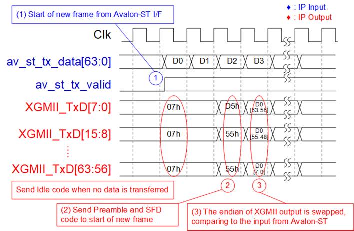
Figure 4: Transmit packet endian
Figure 4 shows more details of the endian relation between the data input from Avalon-ST interface and the data output to XGMII interface. The endian of the data is swapped. After sending Idle code, Preamble, and SFD, byte0 of the 1st Avalon-ST data (D0[7:0]) is placed on XGMII_TxD[63:56], byte1 on XGMII_TxD[55:48], and so on.
Receive Interface
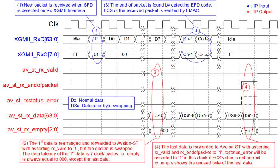
Figure 5: Received packet timing diagram when the 1st data is on byte0
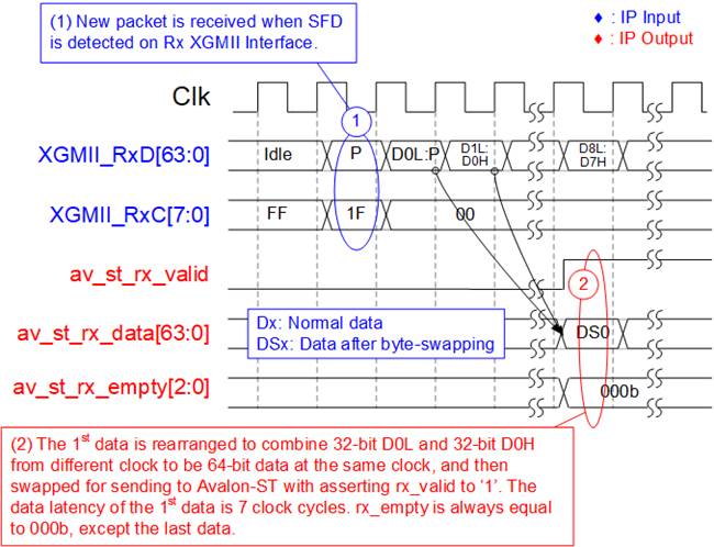
Figure 6: Received packet timing diagram when the 1st data is on byte4
The examples to receive the data stream from XGMII to Avalon-ST are shown in Figure 5 and Figure 6. Two examples are displayed to show the different format of the 1st byte data which may be placed on byte0 or byte4. Though the 1st data is different, the latency of the output (measured from the 1st data) in both examples are similar (7 clock cycles). The details of timing diagram are as follows.
(1) The IP detects SFD code on XGMII interface. The IP rearranges the received packet following the position of the SFD code. The 1st data is placed on the data bus in the next clock which may be valid for 32-bit or 64-bit.
(2) After receiving the 1st data for 7 clock cycles, the IP sends the 1st data which is reformatted to place the 1st byte on byte7 only. The data endian between XGMII and Avalon-ST is swapped, as shown in Figure 7. rx_empty is always equal to 000, except the last data which shows the number of unused bytes.
(3) The IP detects EFD code on XGMII interface. FCS is loaded to compare with the calculated FCS value.
(4) After that, the IP asserts av_st_rx_endofpacket and rx_valid to �1� with the last data on rx_data bus. In this clock, av_st_rxstatus_error will be de-asserted to �0� if the received FCS is equal to the calculated FCS. Otherwise, rxstatus_error is asserted to �1�.
After the IP sends the last data, av_st_rx_valid is de-asserted to �0� at least 1 clock cycle. The gap size of rx_valid is found because preamble, SFD, EFD, and IFG on XGMII interface are removed by EMAC IP.
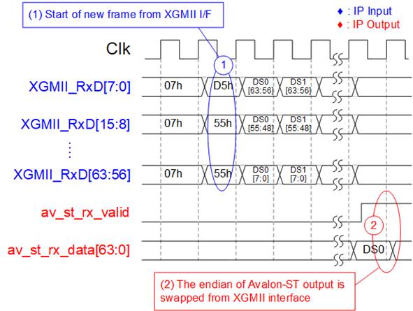
Figure 7: Received packet endian
Similar to Tx path, the endian of the data input from XGMII interface to the data output of Avalon-ST interface is swapped as shown in Figure 7.
Verification Methods
The TenGEMAC IP Core functionality was verified by simulation and also proved on real board design by using Arria10 GX development board and Arria 10 SoC development board.
Recommended Design Experience
User must be familiar with HDL design methodology to integrate this IP into system.
Ordering Information
This product is available directly from Design Gateway Co., Ltd. Please contact Design Gateway Co., Ltd. For pricing and additional information about this product using the contact information on the front page of this datasheet.
Revision History
|
Revision |
Date |
Description |
|
1.0 |
Jul-3-2019 |
New release |
|
1.1 |
2-Oct-2020 |
Update company info |
|
1.2 |
23-Sep-21 |
Add IPVersion port and support on Arria10 SoC development board |