AES256XTSSTG-IP with NVMe-IP Reference design
3 AES256XTSSTGIP reference design
1 Introduction
This document describes detailed of AES256XTSSTGIP, AES256XTSSTG2XIP and AES256XTSSTG4XIP with NVMe IP core reference design. This document will focus on AES256XTSSTGIP, which can serve as a reference for the other modules in the series. The only difference is the width of the data. In this reference design, AES256XTSSTGIP are applied to encrypt data to NVMe SSD and decrypt data from NVMe SSD via NVMeIP. This document will show detail of hardware design and detail of AES256XTSSTGIP in both encryption section and decryption section.
AES256XTSSTGIP reference design is based on NVMe-IP reference design. Users can find the detailed of NVMe-IP reference design from following link: https://dgway.com/NVMe-IP_X_E.html#docs
2 Hardware Overview
The AES256XTSSTGIP reference design is based on the NVMe-IP reference design. Figure 1 shows the block diagram of the NVMe-IP reference design. The operation of NVMe-IP begins when the Test PC sends write or read command parameters to the TestGen module. Subsequently, the TestGen module initiates the writing or reading of pattern data to or from the NVMe SSD via an n-bit FIFO. NVMe-IP handles the management of pattern data between the n-bit FIFO and the NVMe SSD.
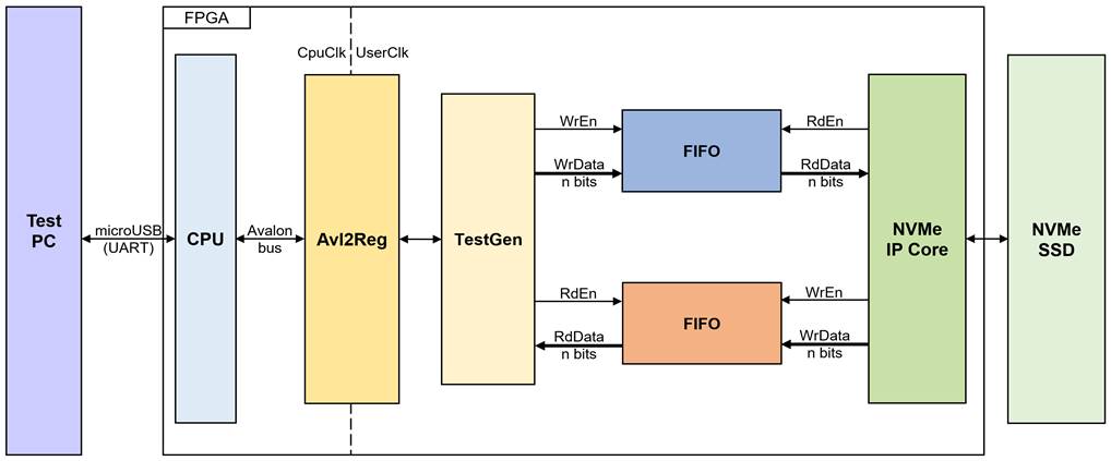
Figure 1 NVMe-IP reference design block diagram
Note: n are integers representing the total data path width.
1) n=128 for AES256XTSSTGIP and NVMe-IP Gen3
2) n=256 for AES256XTSSTG2XIP and NVMeG4-IP or NVMe-IP Gen4
3) n=512 for AES256XTSSTG4XIP and NVMeG5-IP or NVMe-IP Gen5
3 AES256XTSSTGIP reference design
AES256XTSSTGIP reference design has concept to encrypt and decrypt data from or to NVMe SSD. So AES256XTSSTGIP is applied to NVMe-IP reference design as shown in Figure 2. Both FIFO n-bit are replaced by AES256XTSSTGIP. One FIFO is replaced by AES256XTSSTG encryption module (AES256XTSSTGENCTOP), another FIFO is replaced by AES256XTSSTG decryption module (AES256XTSSTGDECTOP).

Figure 2 AES256XTSSTGIP reference design block diagram
In the reference design, dip switches are included to facilitate the change of the key used for encryption and decryption. Specifically, SW6 (GPIO_DIP_SW0 - GPIO_DIP_SW3) are utilized for this purpose. Dip switches are employed to configure the encryption key and tweak key for both AES256XTSSTGENCTOP and AES256XTSSTGDECTOP. The position of the dip switch is shown in Figure 3 and Figure 4.
The configuration of the dip switch is as follows:
1) GPIO_DIP_SW0 and GPIO_DIP_SW1 are responsible for configuring the encryption key (EKEY).
2) GPIO_DIP_SW2 and GPIO_DIP_SW3 are responsible for configuring the tweak key (TKEY).
The specific relationship between the dip switch settings and the encryption key and tweak key configuration as shown in Table 1 and Table 2.
Table 1 Relationship between the dip switch and the encryption key
|
SW1 |
SW0 |
Encryption key Value |
|
0 |
0 |
0x00112233445566778899AABBCCDDEEFF00112233445566778899AABBCCDDEEFF |
|
0 |
1 |
0xFFEEDDCCBBAA99887766554433221100FFEEDDCCBBAA99887766554433221100 |
|
1 |
0 |
0x0000111122223333444455556666777788889999AAAABBBBCCCCDDDDEEEEFFFF |
|
1 |
1 |
0xFFFFEEEEDDDDCCCCBBBBAAAA9999888877776666555544443333222211110000 |
Table 2 Relationship between the dip switch and the tweak key
|
SW3 |
SW2 |
Tweak key Value |
|
0 |
0 |
0x00112233445566778899AABBCCDDEEFF00112233445566778899AABBCCDDEEFF |
|
0 |
1 |
0xFFEEDDCCBBAA99887766554433221100FFEEDDCCBBAA99887766554433221100 |
|
1 |
0 |
0x0000111122223333444455556666777788889999AAAABBBBCCCCDDDDEEEEFFFF |
|
1 |
1 |
0xFFFFEEEEDDDDCCCCBBBBAAAA9999888877776666555544443333222211110000 |
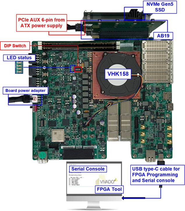
Figure 3 NVMe-IP Gen5 demo setup on VHK158 Evaluation board
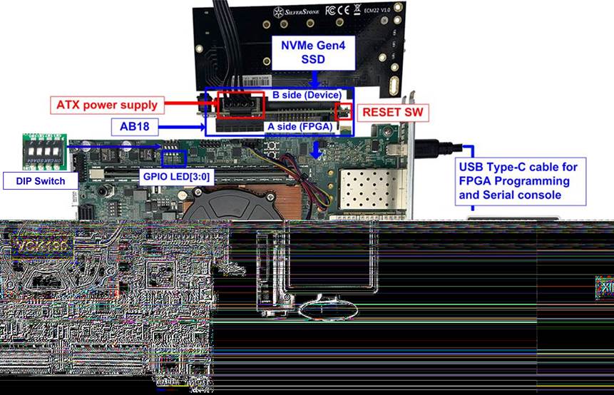
Figure 4 NVMe-IP Gen4 demo setup on VCK190 Evaluation board
3.1 AES256XTSSTGENCTOP
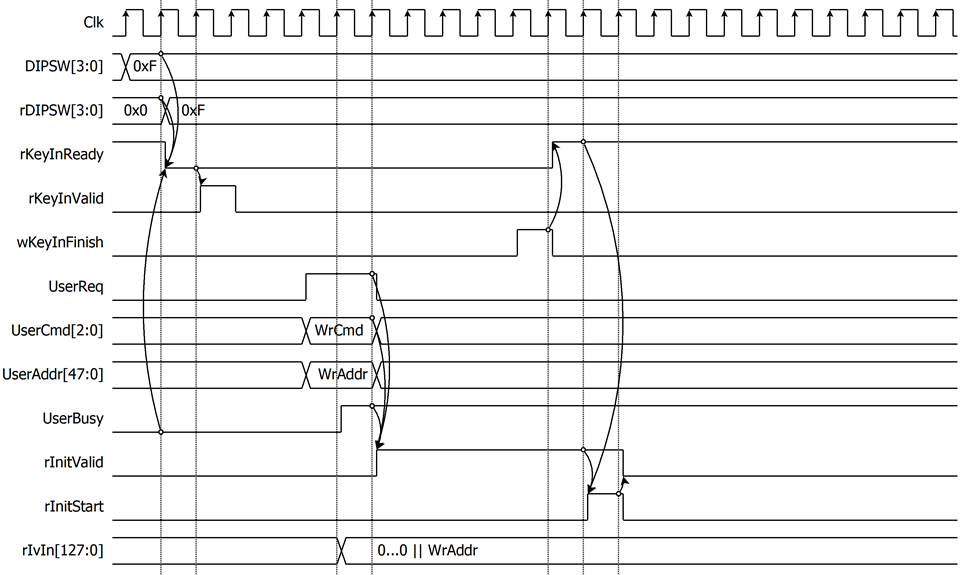
Figure 5 AES256XTSSTGENCTOP block diagram
The AES256XTSSTGENCTOP consists of two n-bit FIFO and one AES256XTSSTGENC, as shown in Figure 5.
3.1.1 Parameter setting
For AES256XTSSTGENC encryption key setting, the process will start when a change in the DIPSW is detected and UserBusy=‘0’, the rKeyInReady will be cleared, and the rKeyInValid will be active only one clock in the next cycle. Once the key generation process is complete, the wKeyInFinish will be active only one clock, and the rKeyInReady will be asserted to ‘1’ in the next cycle. The KeyIn used in the encryption process will change according to the value of the DIPSW, as shown in Table 1 Relationship between the dip switch and the encryption keyTable 1 and Table 2.
The encryption process starts when the user sends a write command to NVMe-IP, as shown in Figure 6. After the NVMe-IP sets UserBusy=‘1’, rInitValid will be asserted to ‘1’, and rIvIn is set to the value of UserAddr with the left-padded zeros. To prevent the loss of NVMe commands, if the user changes the key while sending command. rInitValid is specifically designed to hold the command until the IP is ready for processing. the rInitStart=‘1’ when rInitValid=‘1’ and rKeyInReady=‘1’. The rInitValid will be cleared when rInitStart=‘1’.
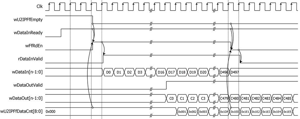
Figure 6 Timing diagram example of encryption parameter setting
3.1.2 Encryption
For encryption process, n-bit plain data, which will be input data for AES256XTSSTGENC, is stored in FIFOIn. FIFOIn has wFfRdEn as the read enable signal of the FIFO, and wFfRdEn is asserted to ‘1’ when FIFOIn is not empty (wU2IPFfEmpty!=‘0’), wDataInReady=‘1’ and the available space of FIFOOut is more than 32 words. rDataInValid is delayed one clock cycle from wFfRdEn. When the wDataOutValid is set to ‘1’, the FIFOOut uses as the write enable signal for the FIFO. The encrypted data is then stored from the wDataOut[n-1:0].
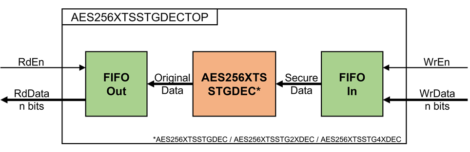
Figure 7 Timing diagram example of data encryption
3.2 AES256XTSSTGDECTOP

Figure 8 AES256XTSSTGDECTOP block diagram
The AES256XTSSTGDECTOP consists of two n-bit FIFO and one AES256XTSSTGDEC, as shown in Figure 7Figure 8.
3.2.1 Parameter setting
For AES256XTSSTGDEC encryption key setting, the process will start when a change in the DIPSW is detected and UserBusy=‘0’, the rKeyInReady will be cleared, and the rKeyInValid will be active only one clock in the next cycle. Once the key generation process is complete, the wKeyInFinish will be active only one clock, and the rKeyInReady will be asserted to ‘1’ in the next cycle. The KeyIn used in the encryption process will change according to the value of the DIPSW, as shown in Table 1 and Table 2.
The decryption process starts when the user sends a read command to NVMe-IP, as shown in Figure 9. After the NVMe-IP sets UserBusy=‘1’, rInitValid will be asserted to ‘1’, and rIvIn is set to the value of UserAddr with the left-padded zeros. To prevent the loss of NVMe commands, if user change the key while sending command. rInitValid is specifically designed to hold the command until the IP ready for processing. the rInitStart=‘1’ when rInitValid=‘1’ and rKeyInReady=‘1’. The rInitValid will be cleared when rInitStart=‘1’.
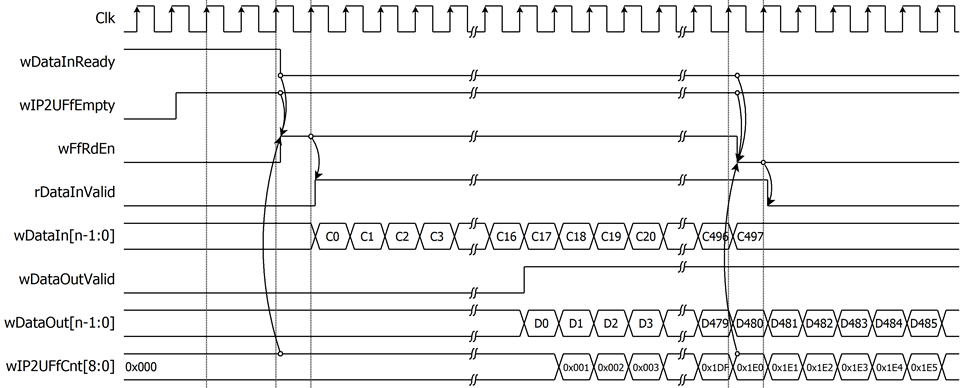
Figure 9 Timing diagram example of decryption parameter setting
3.2.2 Decryption
For decryption process, n-bit cipher data, which will be input data for AES256XTSSTGDEC, is stored in FIFOIn. FIFOIn has wFfRdEn as the read enable signal of the FIFO, and wFfRdEn is asserted to ‘1’ when FIFOIn is not empty (wIP2UFfEmpty!=‘0’), wDataInReady=‘1’ and the available space of FIFOOut is more than 32 words. rDataInValid is delayed one clock cycle from wFfRdEn. When the wDataOutValid is set to ‘1’, the FIFOOut uses as the write enable signal for the FIFO. The decrypted data is then stored from the wDataOut[n-1:0].

Figure 10 Timing diagram example of data decryption
3.3 Auto IV Increment mode
In the reference design example, Full Drive Encryption (FDE) is employed to encrypt all data on the SSD. The Auto IV Increment mode is employed for the purpose of ensuring continuous data encryption. As shown in Figure 11, the data is encrypted using UserAddr (or Logical Block Address - LBA) as the initialization vector (IV). For example, if the user intends to write data and the starting UserAddr/LBA is 0x0000_0000_0123, the first 512 bytes of data will be written to the address 0x0000_0000_0123. Subsequently, the next 512 bytes of data will be written to the address 0x0000_0000_0124, and this pattern will continue until the end of the data.

Figure 11 AES256XTSSTGENCTOP operation timing diagram for AES256XTSSTGIP
In case the user intends to read data and the starting UserAddr/LBA is 0x0000_0000_0124, the first 512 bytes of data will be read from the address 0x0000_0000_0124. Subsequently, the next 512 bytes of data will be read from the address 0x0000_0000_0125, and this pattern will continue until the end of the data.

Figure 12 AES256XTSSTGDECTOP operation timing diagram for AES256XTSSTGIP
4 Example Test Result
The objective is to compare the read and write performance of an 1TB Crucial T700 storage device utilizing AES256XTSSTG4XIP with NVMeIP, as opposed to using NVMeIP alone. The AES256XTSSTG4XIP is fully compatible with NVMeIP. The tests were conducted on a VHK158 Evaluation Board with PCIe Gen5, the data write speeds of around 11000 Mbyte/sec and read speeds of around 8000 Mbyte/sec for both setups.

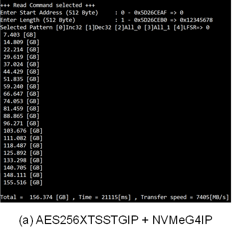
Figure 13 Input and Test result when running Write command
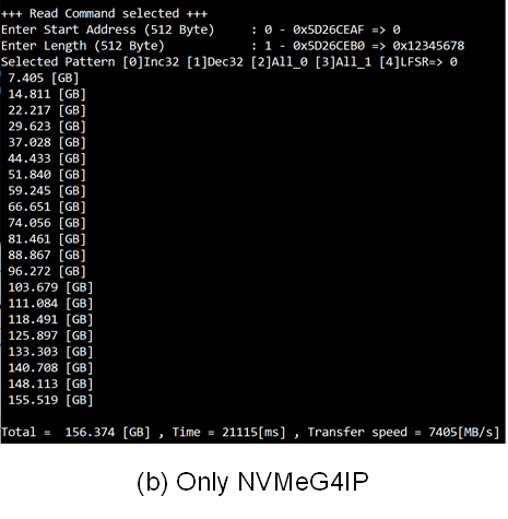
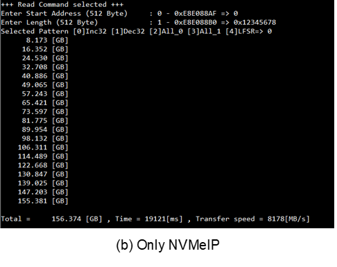
Figure 14 Input and Test result when running Read command
5 Revision History
|
Revision |
Date (D-M-Y) |
Description |
|
1.02 |
16-Sep-24 |
Add information for the reference design on VHK158 |
|
1.01 |
20-Sep-23 |
Update description |
|
1.00 |
25-Aug-23 |
Initial version release |