XXVGMACRSFEC-IP reference design
2.1 25G Ethernet PMA (25G BASE-R)
3.1 Reset EMAC and Transceiver
3.4 Function list in User application
1 Introduction
With the increasing network speeds in data center and industrial systems, errors in data transmission are also becoming more frequent. The reasons for these errors are many, including attenuation over distance in optical cables and equipment quality. To mitigate these errors, the 25Gb Ethernet standard now includes Forward Error Correction (FEC) in the form of Reed-Solomon FEC (RS-FEC). As shown in Figure 1‑1, incorporating RS-FEC into the 25Gb Ethernet standard can enhance the network quality in terms of Bit Error Rate (BER). For instance, the BER of the right system with a value of 10-12 is improved from 5x10⁻⁵ due to the implementation of RS-FEC(1). A BER of 10-12 is considered to be �Nearly free-error� and is commonly used in practice for other Ethernet speed rates.
*(1) Source: https://blogs.cisco.com/sp/25-gigabit-pluggable-transceivers-for-data-center-applications
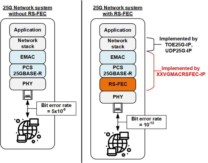
Figure 1‑1 Bit Error Rate in 25Gb network system
Despite the potential increase in system latency that comes with integrating RS-FEC into the Ethernet standard, our XXVGMACRSFEC-IP was specifically designed to address this issue. While RS-FEC is a block coding method, we have ensured that our solution maintains a low-latency system without sacrificing performance, achieving 25G Ethernet as per standard specifications. In addition, our XXVGMACRSFEC-IP includes both MAC and PCS layer logics for 25GBASE-R, enabling seamless integration with our TOE25G-IP and UDP25G-IP solutions for a complete network solution.

Figure 1‑2 Demo system for latency measurement
The purpose of this reference design is to showcase the IP performance in terms of latency. To achieve this, the design utilizes the loopback capability at the physical connection, as shown in Figure 1‑2, to demonstrate round-trip latency. The demo measures latency results from three parts - the XXVGMACRSFEC IP, the Xilinx GTY transceiver, and SFP28 loopback connector - in both transmit and receive directions. Despite the integration of RS-FEC, the average latency of 473.60 ns (as shown in the Figure 1‑2) is relatively low.
However, measuring latency time individually in transmit and receive paths at the physical layer is challenging. As a result, the latency time of the XXVGMACRSFEC IP in transmit and receive paths is obtained through simulation.
The reference design comprises three primary components: the XXVGMACRSFEC IP, the transceiver, and Test logic. The Test logic is applied to measure the round-trip latency of the system, which refers to the time it takes for the first data of a packet to be transmitted and returned.
2 Hardware overview
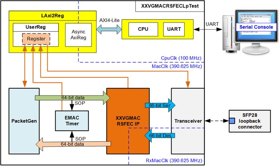
Figure 2‑1 Demo block diagram
The test system utilizes a Serial interface (UART) to connect the CPU on the FPGA with a PC, enabling the user of a Serial console as a user interface. Integrating with XXVGMACRSFEC-IP, the FPGA system can operate the 25G Ethernet system and measure its latency time as the round-trip latency time. During initialization, the system can be configured to operate in two loopback modes. The first mode is an external loopback, which requires an SFP28 loopback module connected to the transceiver operating in normal mode. The second mode is an internal loopback, which is operated by configurating the transceiver to operate Near-End PMA loopback.
The XXVGMACRSFEC-IP is connected to the transceiver for physical data communication, while the user interface of the XXVGMACRSFEC-IP connects to PacketGen, which creates, sends, receives, and verifies test data packets utilizing the physical loopback capability. Additionally, the design includes EMAC Timer to measure the round-trip latency time from the start-of-packet of the transmitted packet to the start-of-packet of the received packet. The CPU firmware controls the register files of UserReg via the AXI4-Lite bus, which is used to control hardware modules or read their status.
The design comprises three clock domains: CpuClk which runs the CPU system, MacClk which is primarily used in the system and applied in the user interface of the IP, and RxMacClk which is used by the IP to interface with the receive interface of the transceiver. The frequency of MacClk and RxMacClk is 390.625 MHz for 25G Ethernet, which is relatively high frequency in the FPGA system. As the purpose of this demo is to showcase round-trip latency, the user logic in this demo operates at MacClk. However, it is recommended to include another clock in the system to run user logic at a lower clock frequency. AsyncAxiReg inside LAxi2Reg is included to facilitate clock domain crossing in the system (CpuClk and MacClk). Further details of each module within the XXVGMACRSFECLpTest are described below.
2.1 25G Ethernet PMA (25G BASE-R)
Xilinx�s GTY Transceiver has been designed to support Physical Medium Attachment (PMA) for 25G BASE-R. To configure the transceiver parameters for the operation of the 25G PMA, Xilinx provides the UltraScale FPGAs Transceivers Wizard. An example configuration of the Xilinx GTY transceiver parameter on the KCU116 board is provided below.
Table 2‑1 Parameter value of Xilinx GTY transceiver
|
Parameter name |
Value |
|
Line Rate (Gb/s) |
25.78125 |
|
PLL type |
QPLL0 |
|
Requested reference clock (MHz) |
156.25 |
|
Actual Reference Clock (MHz) |
322.265625 |
|
Encoding/Decoding |
Async. Gearbox for 64B/66B |
|
User data width |
64 |
|
Internal data width |
64 |
|
TXOUTCLK source |
TXPROGDIVCLK |
|
RXOUTCLK source |
RXPROGDIVCLK |
|
Differential swing and emphasis mode |
Custom |
|
Insertion loss at Nyquist (dB) |
30 |
|
Equalization mode |
Auto |
|
Link coupling |
AC |
|
Termination |
Programmable |
|
Programmable termination voltage (mV ) |
800 |
|
PPM offset between receiver and transmitter |
200 |
For further information on the Transceivers Wizard and GTY Transceiver, please refer to the link provided.
UG573: UltraScale Architecture GTY Transceivers
PG182: UltraScale FPGAs Transceivers Wizard
https://docs.xilinx.com/v/u/en-US/pg182-gtwizard-ultrascale
2.2 XXVGMACRSFEC-IP
The XXVGMACRSFEC-IP is a module that incorporates a 25G Ethernet MAC and an integrated PCS featuring RS-FEC. It connects to a transceiver (PMA) on one end and a user interface on the other. Specifically, the user interface is a 64-bit AXI4-Stream interface.
For additional information, please refer to the datasheet.
https://dgway.com/products/IP/GEMAC-IP/dg_xxvgmacrsfecip_data_sheet_xilinx.pdf
2.3 PacketGen

Figure 2‑2 PacketGen interface
PacketGen is the test logic of XXVGMACRSFEC-IP that comprises two individual logic blocks: TxMAC and RxMAC. The TxMAC logics transmit the data stream to the tx_axis_* interface, which is the 64-bit AXI4 stream standard. On the other hand, the RxMAC logics receive and verify the data stream from the rx_axis_* interface, which is also follow the 64-bit AXI4 stream standard. The UserReg controls and initiates the operation of PacketGen. To commence the data transfer with a specified transfer length, the UserStart is set to 1b with UserLen parameters. For more details information of PacketGen, please refer below.
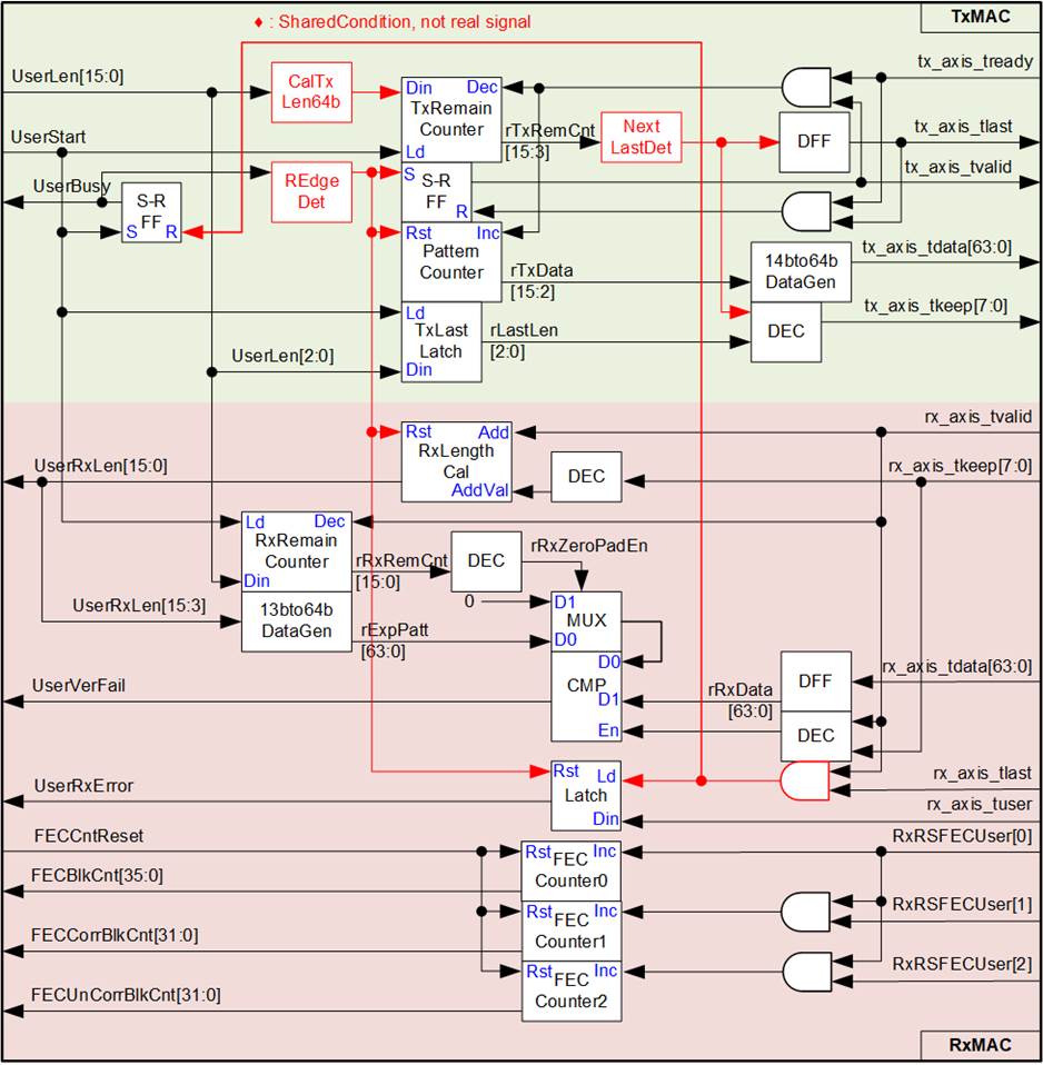
Figure 2‑3 PacketGen block
The PacketGen module�s logic diagram is shown in Figure 2‑3, which comprises two sections: TxMAC on the top and RxMAC at the bottom. Upon setting UserStart to 1b, the busy status (UserBusy) becomes 1b until the last data of the returned packet is received. The rising edge of UserBusy is utilized to reset the internal signals for the new transfer. To generate a transmitted packet until the last data of the packet is completely transferred, tx_axis_tvalid is set to 1b. The TxRamain Counter computes the total amount of transmitted data from the UserLen input. It is decremented after each data is accepted to determine the last beat of Tx packet transmission by setting tx_axis_tlast to 1b. The 64-bit transmitted data (tx_axis_tdata) is formed using a 16-bit incremental pattern that always starts with a zero value. If the packet size is not aligned to 64-bit units (UserLen[2:0] is not equal to 0), the byte valid (tx_axis_tkeep) will not set to an all-one value at the last data. The three lower bits of UserLen are decoded to determine the value of tx_axis_tkeep at the last beat of data transfer.
The loopback logic returns the transmitted packet from the tx_axis_* interface to the rx_axis_* interface. To determine the current amount of data in the received packet, the RxLength Cal decodes the byte valid (rx_axis_tkeep) and the data valid (rx_axis_tvalid), and outputs the result to UserRxLen. UserRxLen is also used to generate the expected 64-bit data (rExpPatt) for comparison with the received data (rx_axis_tdata). In cases where the packet length is less than 60 bytes, the received data includes the zero-padding data. To generate the expected data for comparison with the zero-padding, the RxRemain Counter determines the end of the actual data transfer by decrementing while each data is received. Once all data has been received, rRxZeroPadEn is set to 1b to switch the expected value of received data from the rExpPatt signal to be zero value instead. If the received data does not match the expected value, UserVerFail is set to 1b to indicate the verification error. Upone completion of the received packet, rx_axis_tuser is monitored to detect EMAC errors and assert UserRxError.
Furthermore, the signal quality of the test system can be assessed by monitoring the RxRSFECUser signal, which generates three signals through three counters. The first counter, FECBlkCnt, counts the total number of received RSFEC blocks after FECCntReset is asserted. This counter is incremented when RxRSFECUser[0] is set to 1b. The second counter, FECCorrClkCnt, counts the total number of received RSFEC blocks that contain correctable errors after FECCntReset is asserted. This counter is incremented when both RxRSFECUser[0] and RxRSFECUser[1] are set to 1b. Lastly, the third counter, FECUnCorrBlkCnt, counts the total number of received RSFEC blocks that contain uncorrectable errors after FECCntReset is asserted. This counter is incremented when both RxRSFECUser[0] and RxRSFECUser[2] are set to 1b. If the last counter is not equal to zero, it indicates a potential problem with the test system�s signal quality. Additionally, if the calculated error rate, which is (FECCorrBlkCnt + FECUnCorrClkCnt)/FECBlkCnt, is too high, it also suggests a problem with the signal quality.
Next, the timing diagrams that show the signal details during operation are provided.
Transmit packet

Figure 2‑4 TxMAC timing diagram
1) To initiate packet transmission, UserBusy is set to 1b. The total clock cycles required for transmitting the packet are calculated by reading the UserLen value and using rTxRemCnt. For example, in Figure 2‑4, a 1514-byte packet requires 190 clock cycles (rounding up UserLen/8).
2) When UserBusy rises, the first data is transmitted by setting tx_axis_tvalid to 1b including the first data generated on tx_axis_tdata. Eacg 64-bit data output is created by using the 16-bit data counter, rTxData. While transmitting the packet, tx_axis_tkeep is always set to FFh to indicate 64-bit valid data, except for the last data, which may have fewer valid bytes. The data transfer is continuous by setting tx_axis_tvalid to 1b until the last data is sent.
3) While transmitting each data with both tx_axi_tvalid and tx_axi_tready set to 1b, rTxRemCnt is decremented to indicate the remaining transmitted data, and rTxData is incremented to generate the next value of transmitted data on tx_axis_tdata.
4) If the total amount of data exceeds one, the last data generating is indicated by checking rTxRemCnt=2 and tx_axis_tvalid=1b. The last data is transferred by setting tx_axis_tlast to 1b and setting tx_axis_tkeep to the valid bytes of the last data, decoded from rLastLen[2:0] (the latched value of UserLen[2:0]).
5) XXVGEMACRSFEC-IP then pauses data transmission for 3 or 7 cycles by de-asserting tx_axis_tready to 0b while creating the Ethernet frames.
6) After the loopback logic returns the last data of the packet, the operation is finished, and UserBusy is set to 0b.
Receive packet
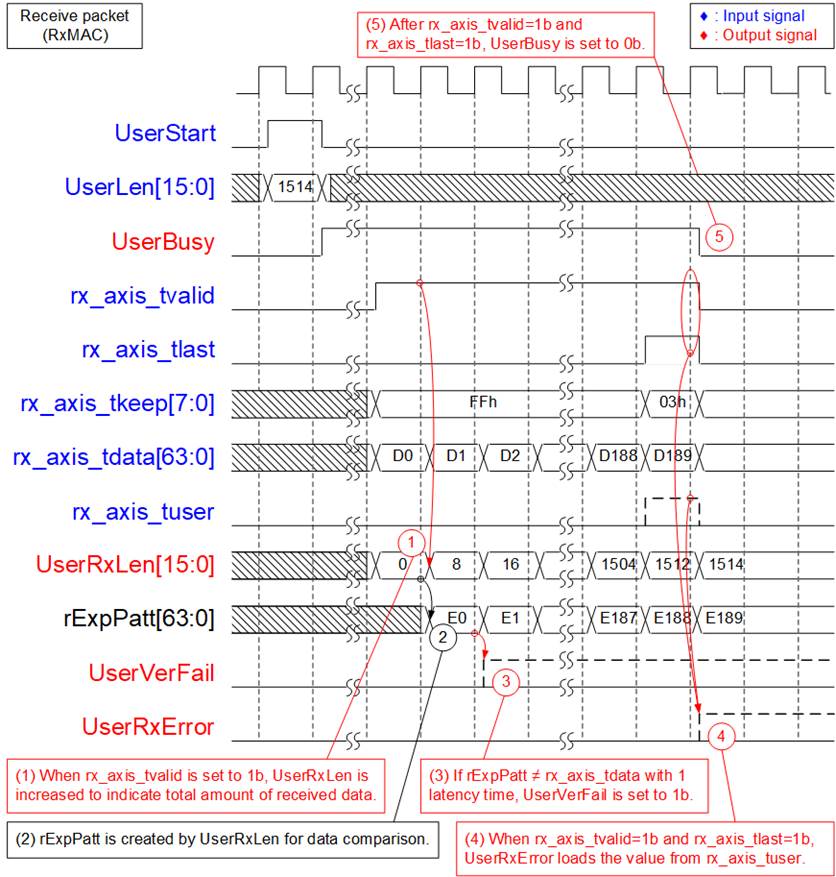
Figure 2‑5 RxMAC Timing diagram
1) The first data of received packet is transferred by setting rx_axis_tvalid to 1b, along with the 64-bit data on rx_axis_tdata and the 8-bit byte enable on rx_axis_tkeep. The packet is continuously transferred by keeping rx_axis_tvalid set to 1b until the last data is transferred. UserRxLen is incremented by 8 for every data, except the last data which has a variable number of valid bytes that must be decoded from the rx_axis_tkeep. UserRxLen is used to count the total amount of received data in byte units.
2) UserRxLen is also used to generate the 64-bit expected data, rExpPatt, for verifying with the received data. The first expected data (E0) is valid the next clock after receiving the first data (D0) on rx_axis_tdata, so it needs to add one clock latency time to the received data for comparing with rExpPatt.
3) If the received data does not match the expected data (rExpPatt), the verification fail flag (UserVerFail) is set to 1b.
4) When the last data of the packet is received, indicated by rx_axis_tvalid and rx_axis_tlast being set to 1b, UserRxError loads its value from rx_axis_tuser. If UserRxError is set to 1b, it means the XXVGMACRSFEC-IP has detected an error on the MAC layer.
5) After the last data of the packet is received, UserBusy is set to 0b and the module returns to Idle status. The module is then ready to receive a new command.
2.4 EMAC Timer
As illustrated in Figure 2‑1, the EMAC Timer is utilized to calculate the round-trip latency of the XXVGMACRSFEC-IP and the transceiver with loopback capability. To achieve loopback, an external loopback module or the transceiver�s internal loopback can be used. The latency time is measured from the transmission of the first data of the Tx packet to the reception of first data of the Rx packet on the XXVGMACRSFEC-IP�s user interface.
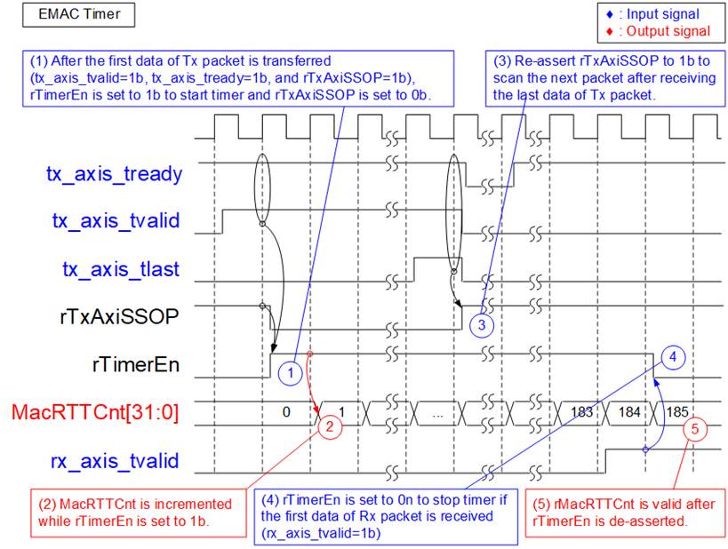
Figure 2‑6 EMAC Timer Timing Diagram
The following details explain the EMAC operation.
1) Initially, rTxAxiSSOP is set to 1b to detect the first data beat of the transmitted packet. After the first data of the Tx packet is transferred (tx_axis_tready=1b, tx_axis_tvalid=1b, and rTxAxiSSOP=1b), rTxAxiSSOP is de-asserted to 0b, and rTimerEn is set to 1b to activate the round-trip latency timer.
2) At the beginning of each operation, the round-trip latency timer (MacRTTCnt) is reset to a zero value. It is incremented every clock cycle while rTimerEn is set to 1b.
3) After the last data of the transmitted packet is transferred (tx_axis_tvalid=1b and tx_axis_tlast=1b and tx_axis_tready=1b), rTxAxiSSOP is re-asserted to 1b to scan the next packet.
4) Once the first data of the received packet is transferred, rTimerEn is set to 0b.
5) At this point, the round-trip latency measurement is completed, and the result of MacRTTCnt is valid, indicating the latency time in clock cycle unit. The CPU reads the MacRTTCnt value, which is then converted to nanoseconds by multiplying it with 2.56 (the time period of 390.625 MHz).
2.5 CPU and Peripherals
The 32-bit AXI4-Lite is used for CPU access to peripherals such as Timer and UART in the test system. Control and status signals are connected to be registers for CPU access as a peripheral through the 32-bit AXI4-Lite bus. The CPU assigns a different base address and address range to each peripheral, allowing access to one peripheral at a time.
In the reference design, the test hardware is connected to the CPU system as a peripheral with a specified base address and range. Therefore, the LAxi2Reg module that interfaces with the CPU must support the AXI4-Lite bus standard for CPU writing and reading, as shown in Figure 2‑7.
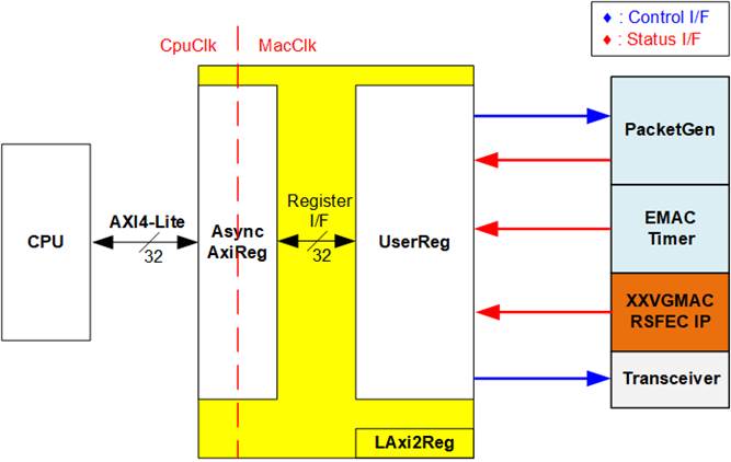
Figure 2‑7 LAxi2Reg block diagram
The LAxi2Reg module includes two parts: AsyncAxiReg and UserReg. AsyncAxiReg is designed to convert the AXI4-Lite signals to a simple Register interface with a 32-bit data bus size, similar to AXI4-Lite data bus size. In addition, AsyncAxiReg includes asynchronous logic to support clock domain crossing between the CpuClk domain and MacClk domain.
UserReg includes the Register file for the parameters and the status signals of the test logics. There are four hardware modules connected to UserReg which are PacketGen, EMAC Timer, XXVGMACRSFEC-IP, and Transceiver. Further details of AsyncAxiReg and UserReg are described below.
2.5.1 AsyncAxiReg

Figure 2‑8 AsyncAxiReg interface
The AXI4-Lite bus interface signals are categorized into five groups: LAxiAw* (Write address channel), LAxiw* (Write data channel), LAxiB* (Write response channel), LAxiAr* (Read address channel), and LAxir* (Read data channel). More information on creating custom logic for the AXI4-Lite bus can be found in the following document.
According to the AXI4-Lite standard, the write channel and read channels operate independently for both control and data interfaces. Therefore, the logic in the AsyncAxiReg module that interfaces with the AXI4-Lite bus is divided into four groups: Write control logic, Write data logic, Read control logic, and Read data logic, as shown on the left side of Figure 2‑8. The Write control I/F and Write data I/F of the AXI4-Lite bus are latched and transferred to become the Write register interface with clock domain crossing registers. Similarly, the Read control I/F of the AXI4-Lite bus is latched and transferred to the Read register interface, while Read data is returned from the Register interface to the AXI4-Lite bus via clock domain crossing registers. In the Register interface, RegAddr is a shared signal for write and read access, loading the value from LAxiAw for write access or LAxiAr for read access.
The Register interface is compatible with a single-port RAM interface for write transaction. However, the read transaction of the Register interface has been slightly modified from the RAM interface by adding the RdReq and RdValid signals to control read latency time. Since the address of the Register interface is shared for both write and read transactions, the user cannot write and read the register simultaneously. The timing diagram of the Register interface is shown in Figure 2‑9.
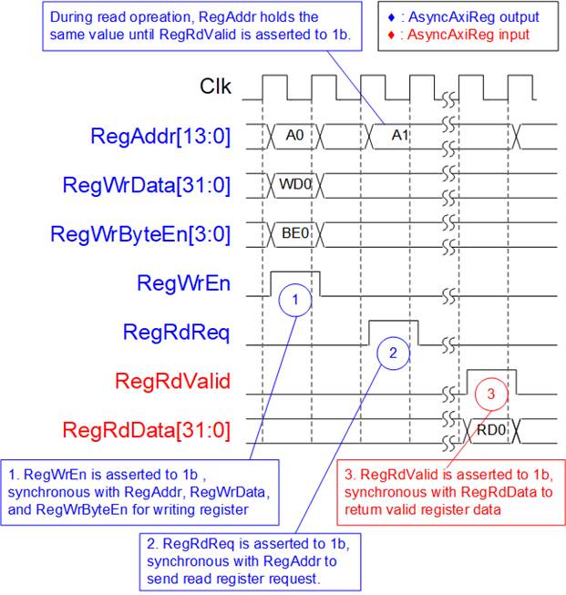
Figure 2‑9 Register interface timing diagram
1) Timing diagram to write register is similar to that of a single-port RAM. The RegWrEn signal is set to 1b, along with a valid RegAddr (Register address in 32-bit units), RegWrData (write data for the register), and RegWrByteEn (write byte enable). The byte enable consists of four bits that indicate the validity of the byte data. For example, bit[0], [1], [2], and [3] are set to 1b when RegWrData[7:0], [15:8], [23:16], and [31:24] are valid, respectively.
2) To read register, AsyncAxiReg sets the RegRdReq signal to 1b with a valid value for RegAddr. The 32-bit data is returned after the read request is received. The slave detects the RegRdReq signal being set to start the read transaction. In the read operation, the address value (RegAddr) remains unchanged until RegRdValid is set to 1b. The address can then be used to select the returned data using multiple layers of multiplexers.
3) The slave returns the read data on RegRdData bus by setting the RegRdValid signal to 1b. After that, AsyncAxiReg forwards the read value to the LAxir* interface.
2.5.2 UserReg
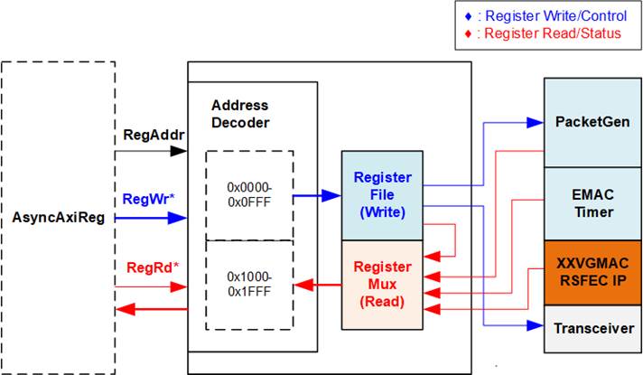
Figure 2‑10 UserReg block diagram
The UserReg module includes the registers for write and read access with four hardware modules: PacketGen, EMAC Timer, XXVGMACRSFEC-IP, and Transceiver. The register file within UserReg has a 32-bit bus size, so write byte enable (RegWrByteEn) is not utilized. When writing to hardware registers, the CPU must use a 32-bit pointer to place a 32-bit valid value onto the write data bus. On the other hand, when the CPU reads the hardware registers, a 32-bit read data is returned. To select the active register for write or read access, the address is decoded by Address Decoder. The address space is divided into two areas, as shown in Figure 2‑10.
1) 0x0000 � 0x0FFF: Write-only access register for the control signals.
2) 0x1000 � 0x1FFF: Read-only access register for the status signals.
The Address Decoder separates the accessing area of the request transaction by decoding the upper bits of RegAddr, while the lower bits are utilized to select the active register in the specific area. Since there is only one status register in UserReg, a single-level multiplexer is applied to select the read data. The latency time of read data is equal to one clock cycle due to the use of one D Flip-flop of RegRdReq to create RegRdValid. More detailed information regarding the address mapping within the UserReg module is presented in Table 2‑2.
Table 2‑2 Register map Definition
|
Address |
Register Name |
Description |
|
Wr/Rd |
(Label in the �xxvgmacrsfeclptest.c�) |
|
|
BA+0x0000 � BA+0x0FFF: User Logic Write Area |
||
|
BA+0x0000 |
User start command |
Wr[0] � Start PacketGen operation by setting 1b. The logic creates and sends the data packet and then waits its return. |
|
Wr |
(USRCMD_INTREG) |
|
|
BA+0x0004 |
Packet length |
Wr[31:0] � Total amount of transmitted data in byte unit. Valid from 1-9014 bytes. |
|
Wr |
(USRTXLEN_INTREG) |
|
|
BA+0x0008 |
MAC Reset |
Wr[0] � Set to 1b for resetting the EMAC module and the transceiver and set to 0b for releasing the reset. |
|
Wr |
(MACRST_INTREG) |
|
|
BA+0x000C |
Loopback mode |
Wr[0] � Set to 1b for enabling the transceiver loopback (Near-end PMA) and set to 0b for using transceiver in normal operation (Use loopback connector). This register affects when only MAC Reset is active. |
|
Wr |
(MACLPBACK_INTREG) |
|
|
BA+0x0010 |
Reset Error Counter |
Wr[0] � Set to 1b to clear all FEC counter value in PacketGen module which can be read from FECBLKL/HCNT_INTREG, FECCORRCLKCNT_INREG, and FECUNCORRBLKCNT_INTREG. |
|
Wr |
(FECCNTRST_INTREG) |
|
|
BA+0x1000 � BA+0x1FFF: User Logic Read Area |
||
|
BA+0x1000 |
User status |
Rd [0] � PacketGen Busy (0b: Idle, 1b: PacketGen module is busy) [1] � Mapped to Linkup signal of XXVGMACRSFEC-IP (1b: Linkup) [2] � Data verification error (0b: Normal, 1b: Error) [3] � Latched Rx MAC error indicator (0b: Normal, 1b: Error) Bit[3:2] are auto-cleared when new operation is started or reset. |
|
Rd |
(USRSTS_BUSY) |
|
|
BA+0x1004 |
Total receive length |
Rd[15:0] � Current amount of received data from XXVGMACRSFEC-IP in byte unit. The value is cleared to 0 when the new operation is started by setting USRCMD_INTREG[0] to 1b. |
|
Rd |
(USRRXLEN_INTREG) |
|
|
BA+0x1010 |
Current receive RSFEC block (Low) |
Rd[31:0] � 32 lower bits (bit[31:0]) of the current number of received RSFEC code blocks |
|
Rd |
(FECBLKLCNT_INTREG) |
|
|
BA+0x1014 |
Current receive RSFEC block (High) |
Rd[3:0] � 4 upper bits (bit[35:32]) of the current number of received RSFEC code blocks |
|
Rd |
(FECBLKHCNT_INTREG) |
|
|
BA+0x1018 |
Current Correctable RSFEC block |
Rd[31:0] � The current number of RSFEC code blocks that contain the correctable error |
|
Rd |
(FECCORRBLKCNT_INTREG) |
|
|
BA+0x101C |
Current Uncorrectable RSFEC block |
Rd[31:0] � The current number of RSFEC code blocks that contain the uncorrectable error |
|
Rd |
(FECUNCORRBLKCNT_INTREG) |
|
|
BA+0x1020 |
Round-trip latency time |
Rd[31:0] � Round-trip latency time in clock cycle unit. The value is measured by a hardware counter from Transmit to Receive path. |
|
Rd |
(USRTIMER_INTREG) |
|
|
BA+0x1800 |
IP version |
Rd[31:0] � Mapped to IPVersion output from XXVGMACRSFEC-IP when the system integrates the IP. Otherwise, it is equal to 0. |
|
Rd |
(IPVER_INTREG) |
|
3 CPU Firmware on FPGA
Upon FPGA boot-up, a welcome message is displayed and user selects the transceiver loopback mode, either external or internal.
· External loopback mode is a normal operation of the transceiver but a loopback connector must be plugged in at the physical interface to initialize the system.
· Internal loopback mode is an optional setting of the transceiver, it is set to �Near-End PMA Loopback�, in which the transmit path is redirected to the receive path within the transceiver itself. This mode does not require any additional equipment to complete the initialization process.
After the user selects the mode, it is registered in the hardware, and both the transceiver and XXVGMACRSFEC-IP are reset. The CPU then waits for the physical layer's initialization by detecting the link up status, which is an output of the IP. More details of this step are described in the Reset EMAC and Transceiver menu (topic 3.1).
Once the IP initialization is complete, a completion message and the Main menu are displayed respectively. In summary, user only selects the transceiver loopback mode and waits for the initialization process. There are three test operations available for the user to select, and more details about each menu are described as follows.

Figure 3‑1 System initialization using External loopback mode
3.1 Reset EMAC and Transceiver
This menu allows the user to change the transceiver loopback mode and also reset both the transceiver and the IP. The sequence of resetting the system is as follows.
1) Ask user to select the transceiver loopback mode, either external or internal.
2) Reset the physical layers, which include the IP and the transceivers, by setting MACRST_INTREG[0] to 1b.
3) Change the transceiver setting by registering the mode in MACLPBACK_INTREG[0].
4) Release the physical layers� reset by setting MACRST_INTREG[0] to 0b.
5) Wait for the IP initialization by monitoring its link up (USRSTS_INTREG[1]=1b).
Note: If the IP initialization takes longer than 5 seconds, a message displaying the link down status is shown. For the external loopback mode, it is often due to the unplugged loopback connector.
6) Display a completion message after all reset sequences and initialization processes are complete.
3.2 Loopback Transfer Test
This menu is designed to measure the IP�s round-trip latency by sending a data packet through the transmit interface and waiting for its return through the receive interface. The PacketGen module creates, sends, and waits for the data packet, and there is a latency measurement part for determining the latency time. The sequence of Loopback Transfer Test is as follows.
1) Ask user for the following test parameters
a) Input packet length: The unit of the packet length is byte and the valid range of value is 1 � 9014 bytes. The input can be decimal unit or hexadecimal unit.
b) Input number of the packets: The number of packets in this test operation and the valid range of value is 1 � 256 packets. The input can be decimal unit or hexadecimal unit.
2) Register the packet length in the hardware by setting USRTXLEN_INTREG[15:0] to the packet length value set by user.
3) Initialize the variables required for the latency calculation, which are the average, minimum, and maximum latency. These variables are initially set to 0, 0xFFFF_FFFF, and 0, respectively.
4) Run the following steps multiple times for the number of packets.
a) Set the start command to the user logic in the hardware by setting USRCMD_INTREG[0] to 1b. Then, USRSTS_BUSY[0] is applied to check whether the operation is complete or not, where 1b means the operation is in progress and 0b means the operation is finished.
b) Check the errors while waiting the user logic to complete its operation by checking the status (USRSTS_INTREG). There�re three cases considered as errors which are the user logic fails to verify the received data, the user logic receives an error indication from the received data, and the link connection is down.
c) After each test, check the received packet length by comparing it with the packet length set by user. In case the set packet length is below 60 bytes, the compared packet length is set to 60 bytes instead due to the zero-padding feature.
d) Update the calculated latency variables.
5) After the tests are finished, �Loopback test complete� is displayed.
6) Calculate and display the latency times and the current transceiver loopback mode.
3.3 Bit Error Rate Test
This menu enables users to check the bit error rate transferring data from the Tx to Rx interface using the loopback circuit. The error rate is calculated by dividing the number of received RSFEC code blocks that contains errors by the total number of received RSFEC code blocks during a specified time. To conduct the Bit Error Rate Test, follow these steps.
1) Ask the user to enter the test duration in seconds, valid from 1 to 10800 (3 hours). The input can be decimal unit or hexadecimal unit.
2) Reset the error counter value in hardware by setting FECCNTRST_INTREG[0] to 1b.
3) Start the timer and wait until the timer reaches the duration specified in step 1). While the timer is running, the user can input certain keys to select one of two options.
a) Press �0� to display the current value of all RSFEC counters by reading
FECBLKH/LCNT_INTREG[3:0], FECCORRBLKCNT_INTREG[31:0], and
FECUNCORRBLKCNT_INTREG[31:0]. After that, display all read values on the console and re-display the two options.
b) Press �1� to exit the test early. After selecting this option, the console will display �Cancel operation� and the test will be terminated.
Once the timer reaches the set duration, the test will end and the console will display �Finish operation�.
4) Display the test result on the console, which include the total runtime, the total number of received RSFEC code blocks, the total number of correctable error RSFEC blocks, and the total number of uncorrectable error RSFEC blocks.
3.4 Function list in User application
This topic describes the function list to run the operation of XXVGMACRSFEC-IP in the loopback demo reference design.
|
int ber_test(void) |
|
|
Parameters |
None |
|
Return value |
0: The operation is successful -1: Receive invalid input or error is found |
|
Description |
Run Bit Error Rate Test following description in topic 3.3. |
|
int check_error(void) |
|
|
Parameters |
None |
|
Return value |
0: No error -1: Errors have been occurred |
|
Description |
Read USRSTS_INTREG register for the user status. If the data verification has failed, the error indication has been received, or the link connection is down, print error messages and then return -1. If none of these conditions are met, return 0 to indicate normal operation. |
|
void show_latency(unsigned int avg, unsigned int min, unsigned int max) |
|
|
Parameters |
avg: Average round-trip time in clock cycle unit min: Minimum round-trip time in clock cycle unit max: Maximum round-trip time in clock cycle unit |
|
Return value |
None |
|
Description |
Display the latency performance by converting the measured latencies from clock cycle unit to nanosecond unit and printing them with two-digit decimals. Additionally, the transceiver loopback mode is displayed to show the current mode of operation. |
|
void wait_ethlink(void) |
|
|
Parameters |
None |
|
Return value |
None |
|
Description |
Read USRSTS_LINKUP[1] to check the link connection status. If the link connection is down, print a message every 5 seconds to indicate that the link connection is still down. This function is applied for blocking the software sequence until the ethernet MAC initialization status is found. |
|
void init_eth(void) |
|
|
Parameters |
None |
|
Return value |
None |
|
Description |
Run Reset EMAC and Transceiver following description in topic 3.1. |
|
int loopback_test(void) |
|
|
Parameters |
None |
|
Return value |
0: The operation is successful -1: Receive invalid input or error is found |
|
Description |
Run Loopback Transfer Test following description in topic 3.2. |
4 Revision History
|
Revision |
Date |
Description |
|
1.0 |
10-Apr-23 |
Initial version release |