TOE10GLL-IP (Cut-through mode) reference design
Rev1.2 3-Jul-23
2.1 Xilinx Transceiver (PMA for 10GBASE-R)
3.6 Function list in User application
4.1 “tcpdatatest” for half duplex test
4.2 “tcp_client_txrx_40G” for full duplex test
1 Introduction
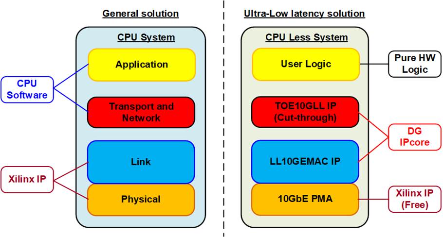
Figure 1‑1 Low-latency solution
The general solution for implementing TCP/IP data processor with FPGA is mostly designed by using CPU system for running TCP/IP stack. While the lower layers - link layer and physical layer, can be implemented by Xilinx IP core which is 10/25G Ethernet Subsystem, as shown on the left side of Figure 1‑1. Though this solution is flexible to design the application on CPU, the result shows much latency time for processing both TCP/IP stack and the application.
To achieve the lowest latency solution, the design on the right side of Figure 1‑1 is designed - the full hardware logic system for processing TCP/IP packet. This solution is fit with the time-sensitive application that implements the user logic by the hardware logic for transferring TCP data with TOE10GLL-IP. TOE10GLL-IP in cut-through mode implements TCP/IP stack with ultra-low latency. Also, it is recommended to connect with the low latency 10G Ethernet MAC IP (LL10GEMACIP) to achieve the lowest latency system. The lowest layer of hardware, PMA layer, is provided by Xilinx as a free PMA IP.
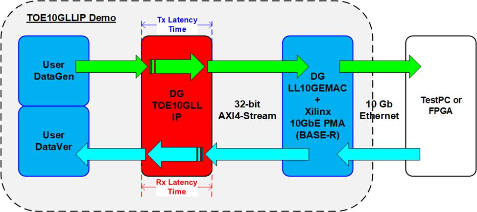
Figure 1‑2 Test logic for TOE10GLL-IP
The simple test logic is designed to show TCP/IP stack implementation with achieving low latency time as shown in Figure 1‑2. User logic can be separated into two parts: UserDataGen and UserDataVer. UserDataGen generates the 32-bit incremental data pattern and transfers to TOE10GLL-IP to build TCP packet. Next, TCP packet is forwarded to LL10GEMAC-IP and Xilinx 10GbE PMA (BASE-R). The target device can be designed by TestPC or another FPGA which runs the same hardware but verifies the received data by UserDataVer. When using TestPC, the test software is run on TestPC for data verification. Besides, the latency time of TOE10GLL-IP when transmitting data is measured by using the timer.
On the other hand, TOE10GLL-IP receives TCP packet from LL10GEMAC-IP and extracts TCP payload data of the valid packet to UserDataVer. UserDataVer verifies TCP payload data that is transmitted by Test software on PC or another FPGA board. Similar to Tx path, the latency time of TOE10GLL-IP when receiving data is measured by the timer. The latency time for both directions is measured from start-of-frame to start-of-frame
CPU system is included for user to interface with hardware logic via Serial console. Network parameters of the test system can be set by the user from the console as well as the parameters of the test logic such as total transfer length and packet size. Also, the test results, latency time, and the progress of test operation, are returned to CPU and then displayed on the console. More details of the demo are described as follows.
2 Hardware overview
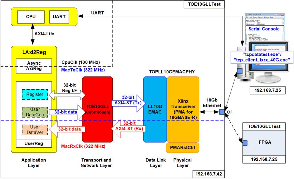
Figure 2‑1 Demo Block Diagram
The test system includes CPU for the ease of user interface and flexibility of test environment. User can set the test parameters such as network parameters and transfer size. Also, the current status of the test system such as current transfer size is displayed on Serial console for monitoring the test progress. To connect the hardware with CPU system, AXI4-Lite bus must be implemented by LAxi2Reg. LAxi2Reg converts AXI4-Lite interface to be the user interface of TOE10GLL-IP module. Also, LAxi2Reg includes AsyncAxiReg - asynchronous module between CpuClk (independent clock for running the CPU system) and MacTxClk (clock output, generated by Xilinx transceiver module).
The user interface of TOE10GLL-IP connects to UserReg within LAxi2Reg module to control and monitor the TOE10GLL-IP operation. UserReg includes UserDataGen and UserDataVer to generate 32-bit test data and verify the received data with TOE10GLL-IP. While Register files inside UserReg are written and read by CPU firmware to set test parameters and read current status of TOE10GLL-IP and the test system. Another side of TOE10GLL-IP is connected to 10G Ethernet MAC controller (LL10GEMAC-IP) by using 32-bit AXI4 stream interface (AXI4-ST). LL10GEMAC-IP implements the Ethernet MAC layer and PCS layer with low latency time. Tx and Rx interface of AXI4-ST are run in the different clock domains: MacTxClk and MacRxClk respectively.
LL10GEMAC-IP provided by Design Gateway requires to run with Xilinx Transceiver which is configured to be PMA module for 10GBASE-R interface. PMARstCtrl is designed to control the reset sequence of Xilinx Transceiver
Another side of 10Gb Ethernet is the target device, Test PC or another FPGA board. When using TestPC, the test application (tcpdatatest and tcp_client_txrx_40G) must be run for transferring TCP data. Otherwise, another FPGA board is applied by implementing TOE10GLL-IP to transfer data in the different direction to show the best performance.
2.1 Xilinx Transceiver (PMA for 10GBASE-R)
PMA IP core for 10Gb Ethernet (BASE-R) can be generated by using Vivado IP catalog. In FPGA Transceivers Wizard, the user uses the following settings.
· Transceiver configuration preset : GT-10GBASE-R
· Encoding/Decoding : Raw
· Transmitter Buffer : Bypass
· Receiver Buffer : Bypass
· User/Internal data width : 32
The example of Transceiver wizard in Ultrascale model is described in the following link.
https://www.xilinx.com/products/intellectual-property/ultrascale_transceivers_wizard.html
2.2 LL10GEMAC
The IP core by Design Gateway implements low-latency EMAC and PCS logic for 10Gb Ethernet (BASE-R) standard. The user interface is 32-bit AXI4-stream bus. Please see more details from LL10GEMAC datasheet on our website.
https://dgway.com/products/IP/Lowlatency-IP/dg_ll10gemacip_data_sheet_xilinx_en.pdf
2.3 PMARstCtrl
When the buffer inside Xilinx Transceiver is bypassed, the user logic must control reset signal of Tx and Rx buffer. The module is designed by state machine to run following step.
(1) Assert Tx reset of the transceiver to ‘1’ for one cycle.
(2) Wait until Tx reset done, output from the transceiver, is asserted to ‘1’.
(3) Finish Tx reset sequence and de-assert Tx reset to allow the user logic beginning Tx operation.
(4) Assert Rx reset to the transceiver.
(5) Wait until Rx reset done is asserted to ‘1’.
(6) Finish Rx reset sequence and de-assert Rx reset to allow the user logic beginning Rx operation.
2.4 TOE10GLL
TOE10GLL-IP is the IP core provided by Design Gateway to implement the TCP/IP stack and offload engine for the low latency solution. User interface has two signal groups, i.e., control signals and data signals. The IP can be configured to run in two modes, i.e., Cut-through mode for low-latency application and Simple mode for simple user interface. This reference design shows the usage in Cut-through mode. More details are described in datasheet.
https://dgway.com/products/IP/Lowlatency-IP/dg_toe10gllip_data_sheet_xilinx_en.pdf
2.5 CPU and Peripherals
32-bit AXI4-Lite is applied to be the bus interface for the CPU accessing the peripherals such as Timer and UART. To control and monitor the test system, the control and status signals are connected to register for CPU access as a peripheral through 32-bit AXI4-Lite bus. CPU assigns the different base address and the address range to each peripheral for accessing one peripheral at a time.
In the reference design, the CPU system is built with one additional peripheral to access the test logic. Therefore, the hardware logic must be designed to support AXI4-Lite bus standard for CPU write access and read access. LAxi2Reg module is designed to connect the CPU system as shown in Figure 2‑2.
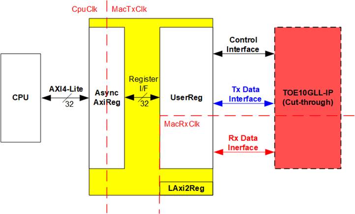
Figure 2‑2 LAxi2Reg block diagram
LAxi2Reg consists of AsyncAxiReg and UserReg. AsyncAxiReg is designed to convert the AXI4-Lite signals to be the simple register interface which has 32-bit data bus size (similar to AXI4-Lite data bus size). Besides, AsyncAxiReg includes asynchronous logic to support clock crossing between CpuClk domain and MacTxClk domain. Tx data interface and Rx data interface of TOE10GLL-IP are run in different clock domain, MacTxClk and MacRxClk. Therefore, UserReg module consists of the logics which run in two clock domains.
UserReg includes the register file of the parameters and the status signals of test logics, including TOE10GLL-IP. Both data interface and control interface of TOE10GLL-IP are connected to UserReg. More details of AsyncAxiReg and UserReg are described as follows.
2.5.1 AsyncAxiReg

Figure 2‑3 AsyncAxiReg Interface
The signal on AXI4-Lite bus interface can be split into five groups, i.e., LAxiAw* (Write address channel), LAxiw* (Write data channel), LAxiB* (Write response channel), LAxiAr* (Read address channel), and LAxir* (Read data channel). More details to build custom logic for AXI4-Lite bus are described in following document.
According to AXI4-Lite standard, the write channel and the read channel are operated independently. Also, the control and data interface of each channel are run separately. The logic inside AsyncAxiReg to interface with AXI4-Lite bus is split into four groups, i.e., Write control logic, Write data logic, Read control logic, and Read data logic as shown in the left side of Figure 2‑3. Write control I/F and Write data I/F of AXI4-Lite bus are latched and transferred to be Write register interface with clock domain crossing registers. Similarly, Read control I/F of AXI4-Lite bus are latched and transferred to be Read register interface. While the returned data from Register Read I/F is transferred to AXI4-Lite bus by using clock domain crossing registers. In register interface, RegAddr is shared signal for write and read access. Therefore, it loads the address from LAxiAw for write access or LAxiAr for read access.
The simple register interface is compatible with single-port RAM interface for write transaction. The read transaction of the register interface is slightly modified from RAM interface by adding RdReq and RdValid signals for controlling read latency time. The address of register interface is shared for write and read transaction, so user cannot write and read the register at the same time. The timing diagram of the register interface is shown in Figure 2‑4.
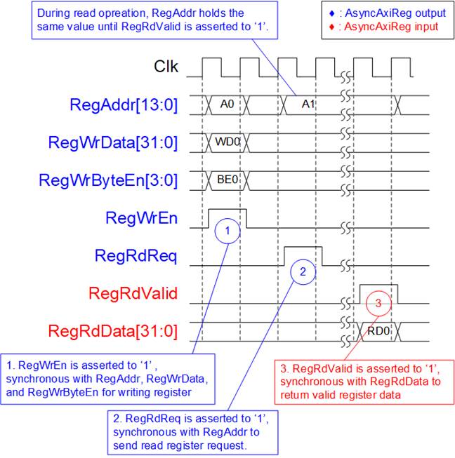
Figure 2‑4 Register interface timing diagram
1) To write register, the timing diagram is similar to single-port RAM interface. RegWrEn is asserted to ‘1’ with the valid signal of RegAddr (Register address in 32-bit unit), RegWrData (write data of the register), and RegWrByteEn (the write byte enable). Byte enable has four bits to enable 4-byte data. Bit[0], [1], [2], and [3] are equal to ‘1’ when RegWrData[7:0], [15:8], [23:16], and [31:24] are valid respectively.
2) To read register, AsyncAxiReg asserts RegRdReq to ’1’ with the valid value of RegAddr. 32-bit data is returned after receiving the read request. The slave detects RegRdReq asserted to start the read transaction. During read operation, the address value (RegAddr) does not change until RegRdValid is asserted to ‘1’. Therefore, the address can be used for selecting the returned data by using multiple levels of multiplexer.
3) The read data is returned on RegRdData bus by the slave with asserting RegRdValid to ‘1’. After that, AsyncAxiReg forwards the read value to LAxir* interface.
2.5.2 UserReg
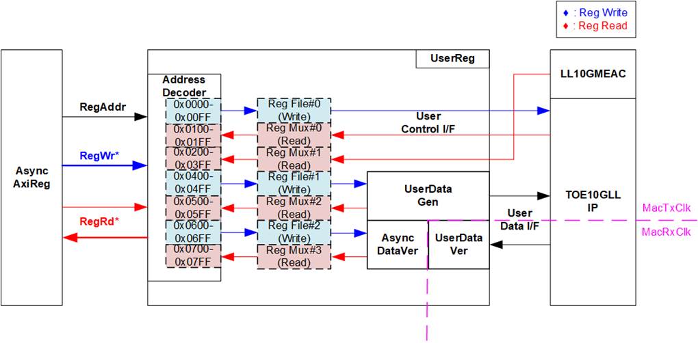
Figure 2‑5 UserReg block diagram
The logic inside UserReg consists of three operations, i.e., Register interface (Address decoder, RegFile, and RegMux), Data pattern generator (UserDataGen), and Data pattern verification (UserDataVer and AsyncDataVer).
Register block decodes the address which is requested from AsyncAxiReg and then selects the active register for write or read transaction. UserDataGen sends 32-bit test data to TOE10GLL-IP for write data interface while UserDataVer block reads and verifies 32-bit data from TOE10GLL-IP for read data interface following AXI4-Stream interface standard. AsyncDataVer is asynchronous circuit of UserDataVer which is run in MacRxClk domain to interface with other modules which are run in MacTxClk domain and vice versa. More details of Register block, UserDataGen, and UserDataVer are described as follows.
Register Block
The address range assigned in UserReg is split into four areas for four hardware logics.
· 0x0000 – 0x01FF: TOE10GLL-IP
· 0x0200 – 0x03FF: LL10GEMAC-IP
· 0x0400 – 0x05FF: UserDataGen
· 0x0600 – 0x07FF: UserDataVer
Address decoder decodes the upper bit of RegAddr for selecting the active hardware that is TOE10GLL-IP, LL10GEMAC-IP, UserDataGen, or UserDataVer. The register file inside UserReg is 32-bit bus size. Therefore, write byte enable (RegWrByteEn) is not applied in the test system and the CPU uses 32-bit pointer to set the hardware register.
To read register, multi-level multiplexers (mux) select the data to return to CPU by using the address. The lower bit of RegAddr is fed to the submodule to select the active data from each submodule. While the upper bit is applied in UserReg to select the returned data from each submodule. Totally, the latency time of read data is equal to two clock cycles. Therefore, RegRdValid is created by RegRdReq with asserting two D Flip-flops. More details of the address mapping within UserReg module are shown in Table 2‑1.
Table 2‑1 Register map Definition
|
Address |
Register Name |
Description |
|
Wr/Rd |
(Label in “toe10glltest.c”) |
|
|
BA+0x0000 – BA+0x01FF: TOE10GLL-IP interface BA+0x0200 – BA+0x03FF: LL10GEMAC-IP interface More details of each signal are described in TOE10GLL-IP and LL10GEMAC-IP datasheet. |
||
|
BA+0x0000 – BA+0x00FF: Input signals of TOE10GLL-IP (Write access only) |
||
|
BA+0x0000 |
TOE_RST_INTREG |
[0]: Mapped to RstB of TOE10GLL-IP |
|
BA+0x0004 |
TOE_OPM_INTREG |
[1:0]: Mapped to DstMacMode of TOE10GLL-IP [16]: Mapped to ARPICMPEn of TOE10GLL-IP |
|
BA+0x0008 |
TOE_SML_INTREG |
[31:0]: Mapped to SrcMacAddr[31:0] of TOE10GLL-IP |
|
BA+0x000C |
TOE_SMH_INTREG |
[15:0]: Mapped to SrcMacAddr[47:32] of TOE10GLL-IP |
|
BA+0x0010 |
TOE_DMIL_INTREG |
[31:0]: Mapped to DstMacAddr[31:0] of TOE10GLL-IP |
|
BA+0x0014 |
TOE_DMIH_INTREG |
[15:0]: Mapped to DstMacAddr[47:32] of TOE10GLL-IP |
|
BA+0x0018 |
TOE_SIP_INTREG |
[31:0]: Mapped to SrcIPAddr of TOE10GLL-IP |
|
BA+0x001C |
TOE_DIP_INTREG |
[31:0]: Mapped to DstIPAddr of TOE10GLL-IP |
|
BA+0x0020 |
TOE_TMO_INTREG |
[31:0]: Mapped to TimeOutSet of TOE10GLL-IP |
|
BA+0x0040 |
TOE_CMD_INTREG |
[1:0]: Mapped to TCPCmd of TOE10GLL-IP. When this register is written, TCPCmdValid of TOE10GLL-IP is asserted to ‘1’ for one cycle. |
|
BA+0x0044 |
TOE_SPN_INTREG |
[15:0]: Mapped to TCPSrcPort[15:0] of TOE10GLL-IP |
|
BA+0x0048 |
TOE_DPN_INTREG |
[15:0]: Mapped to TCPDstPort[15:0] of TOE10GLL-IP |
|
BA+0x0080 |
TOE_TIC_INTREG |
[0]: Set ‘1’ to clear read value of TOE_STS_INTREG[2] (TOE10GLL-IP interrupt) |
|
BA+0x0100 – BA+0x01FF: Output signals of TOE10GLL-IP (Read access only) |
||
|
BA+0x0100 |
TOE_VER_INTREG |
[31:0]: Mapped to IP version of TOE10GLL-IP |
|
BA+0x0104 |
TOE_STS_INTREG |
[0]: Mapped to InitFinish of TOE10GLL-IP [1]: Mapped to TCPConnOn of TOE10GLL-IP [2]: TOE10GLL-IP Interrupt. Asserted to ‘1’ when IPInt of TOE10GLL-IP is asserted to ‘1’. This flag is cleared by TOE_TIC_INTREG. [20:16]: Mapped to IPState of TOE10GLL-IP |
|
BA+0x0108 |
TOE_INT_INTREG |
[31:0]: Mapped to IntStatus of TOE10GLL-IP |
|
BA+0x010C |
TOE_DMOL_INTREG |
[31:0]: Mapped to DstMacAddrOut[31:0] of TOE10GLL-IP |
|
BA+0x0110 |
TOE_DMOH_INTREG |
[15:0]: Mapped to DstMacAddrOut[47:32] of TOE10GLL-IP |
|
BA+0x0200 – BA+0x03FF: Output signals of LL10GEMAC-IP (Read access only) |
||
|
BA+0x0200 |
EMAC_VER_INTREG |
[31:0]: Mapped to IP version of DG LL10GEMAC-IP |
|
BA+0x0204 |
EMAC_STS_INTREG |
[0]: Mapped to Linkup of LL10GEMAC-IP |
|
Address |
Register Name |
Description |
|
Wr/Rd |
(Label in “toe10glltest.c”) |
|
|
BA+0x0400 – BA+0x07FF: UserDataGen and UserDataVer interface |
||
|
BA+0x0400 – BA+0x04FF: Input signals of UserDataGen (Write access only) |
||
|
BA+0x0400 |
USRTX_CMD_INTREG |
[0]: Start flag to generate test data by UserDataGen. Set ‘1’ to start sending data. This flag is auto-cleared after running the operation. [1]: Set ‘1’ to clear USRTX_LENL/H_INTREG and USRTX_TMR_INTREG. |
|
BA+0x0420 |
USRTX_PKL_INTREG |
[10:0]: Packet length in byte unit for assigning TCPTxPkLen, input of TOE10GLL-IP. |
|
BA+0x0424 |
USRTX_PSH_INTREG |
[0]: PSH flag for assigning TCPTxPSH, input of TOE10GLL-IP |
|
BA+0x0428 |
USRTX_TDL_INTREG |
[31:0]: Bit[31:0] of total size in byte unit to generate test data by UserDataGen. The value is cleared by USRTX_CMD_INTREG[1]. |
|
BA+0x042C |
USRTX_TDH_INTREG |
[15:0]: Bit[47:32] of total size in byte unit to generate test data by UserDataGen. The value is cleared by USRTX_CMD_INTREG[1]. |
|
BA+0x0500 – BA+0x05FF: Output signals of UserDataGen (Read access only) |
||
|
BA+0x0500 |
USRTX_STS_INTREG |
[0]: Busy signal of UserDataGen (‘0’-Idle, ‘1’-Data is transmitting) |
|
BA+0x0504 |
USRTX_TMR_INTREG |
Timer value which shows latency time in Tx interface of TOE10GLL-IP [15:0]: Tx latency time of TOE10GLL-IP in clock cycle unit The value is cleared by USRTX_CMD_INTREG [1]. |
|
BA+0x0508 |
USRTX_LENL_INTREG G |
[31:0]: Bit[31:0] of complete size of transmitted data in byte unit which is calculated by the sum of TCPTxCplLen, output from TOE10GLL-IP. The value is cleared by USRTX_CMD_INTREG [1]. |
|
BA+0x050C |
USRTX_LENH_INTREG |
[15:0]: Bit[47:32] of complete size of transmitted data in byte unit which is calculated by the sum of TCPTxCplLen, output from TOE10GLL-IP. The value is cleared by USRTX_CMD_INTREG [1]. |
|
BA+0x0600 – BA+0x06FF: Input signals of UserDataVer (Write access only) |
||
|
BA+0x0600 |
USRRX_CMD_INTREG |
[0]: Enable data verification of UserDataVer (‘0’: Disable data verification, ‘1’: Enable data verification) [1]: Set ‘1’ to clear USRRX_LENL/H_INTREG and USRRX_TMR_INTREG are reset. |
|
BA+0x0604 |
USRRX_RXC_INTREG |
[0]: Set ‘1’ to clear read value of USRRX_STS_INTREG[1] (TCPRxError of TOE10GLL-IP) |
|
BA+0x0700 – BA+0x07FF: Output signals of UserDataVer (Read access only) |
||
|
BA+0x0700 |
USRRX_STS_INTREG |
[0]: Verify fail (‘0’-No error, ‘1’-Received data is incorrect) [1]: Receive error interrupt. Asserted to ‘1’ when TCPRxError from TOE10GLL-IP shows error status. This flag can be cleared by. USRRX_RXC_INTREG. |
|
BA+0x0704 |
USRRX_TMR_INTREG |
Timer value which shows latency time in Rx interface of TOE10GLL-IP [15:0]: Rx Latency time of TOE10GLL-IP in clock cycle unit. The value is cleared by USRRX_CMD_INTREG[1]. |
|
BA+0x0708 |
USRRX_ERR_INTREG |
[7:0]: Latch signal of TCPRxError, output of TOE10GLL-IP. The value does not change after detecting error. The value is reset after this register is read by CPU. |
|
BA+0x0720 |
USRRX_LENL_INTREG |
[31:0]: Bit[31:0] of current size of received data in byte unit which is counted when the packet received from TOE10GLL-IP is valid. The value is cleared by USRRX_CMD_INTREG[1]. |
|
BA+0x0724 |
USRRX_LENH_INTREG |
[15:0]: Bit[47:32] of current size of received data in byte unit which is counted when the packet received from TOE10GLL-IP is valid. The value is cleared by USRRX_CMD_INTREG [1]. |
|
BA+0x0728 |
USRRX_FAILPOSL_INTREG |
[31:0]: Bit[31:0] of the first position in byte unit that data verification detects failure. The value is cleared by USRRX_CMD_INTREG [1]. |
|
BA+0x072C |
USRRX_FAILPOSH_INTREG |
[15:0]: Bit[47:32] of the first position in byte unit that data verification detects failure. The value is cleared by USRRX_CMD_INTREG [1]. |
|
BA+0x0730 |
USRRX_EXPPAT_INTREG |
[31:0]: Expected data that IP should receive when data verification is failed. |
|
BA+0x0734 |
USRRX_RDPAT_INTREG |
[31:0]: Received data which is an incorrect data when data verification is failed. |
User Data Generator
After start signal is asserted by user (TrnStart=’1’), UserDataGen loads the parameters from user (Total data size and packet size) and then starts generating the test data by using 32-bit incremental pattern. Also, checksum is calculated to be TOE10GLL-IP input in Cut-through mode. Busy signal (TrnBusy) is designed for user monitoring the operation. It is de-asserted to ‘0’ when the module finishes the operation.

Figure 2‑6 UserDataGen block
There are two state machines in UserDataGen for controlling Write interface of FIFO (Write S/M) and Read interface of FIFO (Read S/M) respectively. Two FIFOs are applied to store packet size with checksum (PkFifo) and data (DataFifo). After user asserts start flag (TrnStart), UserDataGen asserts busy signal (TrnBusy). The user parameters (PSHFlagSet, PacketSizeSet, and TotDataLenSet) are loaded to the logic. CalPac/CalLen module reads the packet size and total transfer size to calculate the packet size (rCurPkLenLat) for generating to TOE10GLL-IP and the remaining transfer size (rRemTotDataCnt).
Write FIFO interface
The calculated packet size (rCurPkLenLat) is loaded to be initial value of the packet counter (WrPacCount) to control the number of generated data in each packet. After the final data is generated to DataFifo, Write S/M writes 16-bit data checksum of a packet (rDataCSum) and 11-bit packet size (rCurPkLenLat) to PkFIFO. After that, Write S/M checks the remained transfer size (rRemTotDataCnt) and decides to generate the next packet or complete the operation. If there is remained transfer size, it waits until PkFifo is not full before starting the next packet generating. Otherwise, the process is finished. The packet size of every packet except the final packet is equal to PacketSizeSet. While the packet size of the final packet is equal to the remained transfer size (rRemTolDataCnt).
When Write S/M stays in stWrData, the test data is generated by TestPatt Count. The test data must be re-aligned following the byte offset when the packet size is not aligned to 32-bit. The re-aligned data is stored to DataFifo and fed to CSumCal to calculate data checksum of each packet. Write enable of DataFifo is de-asserted when DataFifo has too less free space, monitored by data_count. After the final data of a packet is generated, the complete flag of data checksum calculation (DataCsumCalEn) is asserted. The complete flag is fed to be write enable of PkFifo.
Read FIFO interface
The read FIFO operation begins when PkFIFO is not empty (empty=’0’). PkFifo is read by asserting PkFfRdEn as the first step. The read data of PkFifo is loaded to RdPacCount and latch the be output to the IP (TCPTxPkLen and TCPTxCSum). After that, Read S/M changes to stRdTrn to read one packet data from DataFifo and forward to TOE10GLL-IP by asserting DataFfRdAck. DataFifo is FWFT type, so TCPTxData which is read data of DataFifo is valid at the same time as DataFfRdAck asserted. TCPTxValid is asserted to ‘1’ to send one data packet continuously until finishing one packet transmission. Data transferring is paused when the IP is not ready (TCPTxReady=’0’). RdPacCount is the counter to check the remained size of each packet. When the next data is the final data of a packet, TCPTxEOP is prepared and then asserted to ‘1’ at the same time as the final data transmitted. Also, TCPTxByteEn is calculated from the packet size to be the byte enable of the final data. TCPTxByteEn of other data in a packet is always equal to 1111b.

Figure 2‑7 Write FIFO I/F of UserDataGen timing diagram
1) The operation begins when user asserts TrnStart to ‘1’. The state changes to stWrChkLen and TrnBusy is asserted to ‘1’. At the same time, the input parameters such as TotDataLenSet and PacketSizeSet are loaded to the internal logic.
2) rCurPkLenLat calculates the packet size which is equal to PacketSizeSet for every packet which is not the last packet. After that, the state changes to stWrLdSize.
3) rWrRemPkCnt loads the initial value from rCurPkLenLat and the state changes to stWrData to start generating data.
4) wDataFfWrEn is asserted to ‘1’ when rDataFfWrAFull=’0’ (DataFifo is not full) and the state is stWrData. After wDataFfWrEn is asserted, rDataFfWrEn is asserted to ‘1’ and rDataFfWrData is created to store to DataFifo.
5) When DataFifo shows full status (rDataFfWrAFull=’1’), wDataFfWrEn is de-asserted to ‘0’ to pause generating test data. Next, rDataFfWrEn is de-asserted and rDataFfWrData holds the same value.
6) After the final data of a packet is generated (rWrRemPkCnt=1 and wDataFfWrEn=’1’), the state changes to stWtCSum. Also, the complete flag to calculate data checksum (rDataCsumCalEn[0]) is asserted to ‘1’.
7) After data checksum post-processing is finished (rDataCsumCalEn[4]: 4-clock cycle latency time of rDataCSumCalEn[0] is asserted to ‘1’), the state completes the current loop operation. The state returns to stWrChkLen and rRemTotDataCnt is decreased by the completed packet size.
8) If the remained transfer size (rRemTotDataCnt) is not equal to 0, the state changes to stWrLdSize for starting the next loop. When the current loop is the final loop, rCurPkLenLat loads the packet size from the remained transfer size (rRemTotDataCnt).
9) If the remained transfer size (rRemTotDataCnt) is equal to 0, the state waits until all data in DataFifo is transferred to TOE10GLL-IP completely (DataFfEmpty=’1’). After that, the state returns to stWrIdle and TrnBusy is de-asserted to ‘0’.
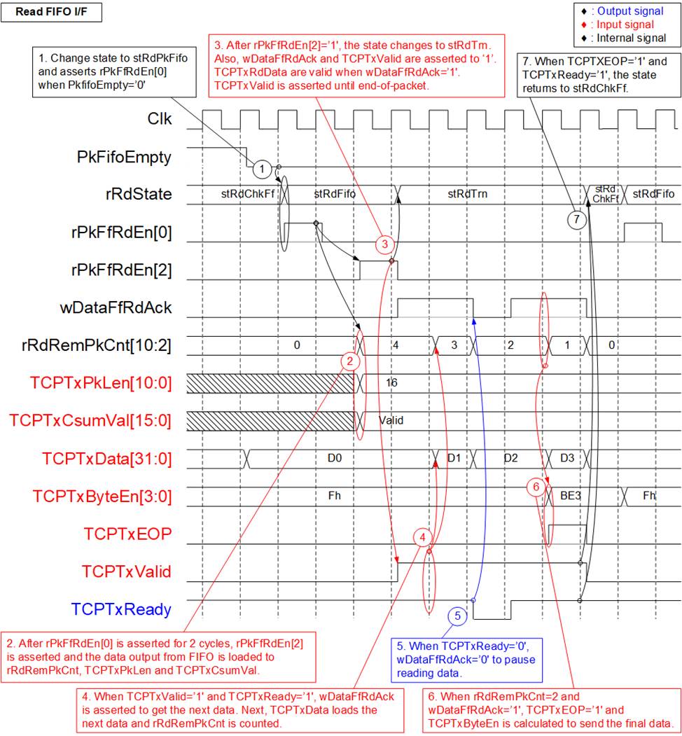
Figure 2‑8 Read FIFO I/F of UserDataGen timing diagram
1) Read operation begins when PkFifo is not empty (PkFifoEmpty=’0’). The state changes to stRdFifo. At the same time, asserts the read enable to PkFifo (rPkFfRdEn[0]=’1’) to read the packet information (11-bit packet size and 16-bit data checksum).
2) After asserting rPkFfRdEn[0] for 2 clock cycles (rPkFfRdEn[2]=’1’), the read data of PkFifo is loaded to be IP output (TCPTxPkLen - packet size, TCPTxCsumVal – data checksum) and the initial value of internal packet counter (rRdRemPkCnt). rPkFfRdEn[2] is applied to show packet information is loaded completely.
3) After rPkFfRdEn[2] is asserted to ‘1’, the state changes to stRdTrn. In this state, one packet data is read from DataFifo and forwarded to TOE10GLL-IP. TCPTxValid is asserted to ‘1’ and the read data of DataFifo is mapped to be TCPTxData (data output to TOE10GLL-IP). Also, read acknowledge of DataFifo (wDataFfAck) is asserted to ‘1’ to get the next data when the state is stRdTrn and the IP accepts the data (TCPTxReady=’1’).
4) When wDataFifo is asserted to ‘1’, the packet counter (rRdRemPkCnt) is down-counted. Also, the next data (D1) is read from DataFifo.
5) If TOE10GLL-IP is not ready to receive data by de-asserting TCPTxReady to ‘0’, wDataFfRdAck is de-asserted to ‘0’ to pause transmitting data. Therefore, TCPTxData holds the same value.
6) When the next data is the final data of a packet (rRdRemPkCnt=2 and wDataFfRdAck=’1’), TCPTxEOP is asserted to ‘1’ and the final data (D3) is transmitted to TOE10GLL-IP.
7) After the final data is transferred completely (TCPTxEOP=’1’ and TCPTxReady=’1’), the state changes to stRdChkFf. Also, TCPTxValid is de-asserted to ‘0’. If PkFifo still has the next packet information, repeat step 1) to start forwarding the next packet.
User Data Verification
UserDataVer receives the data from TOE10GLL-IP and then verifies the value if verification enable (VerifyEn) is set to ‘1’ by the user. The expected pattern is 32-bit incremental pattern. The received packet from TOE10GLL-IP may have the error when the signal quality of ethernet connection is bad condition to make the packet broken. If the packet error is found, the expected data for data verification reloads the value to start from the latest position which receives the valid packet.
Note: When the received packet is error, TOE10GLL-IP starts the data recovery process. After that, the same data packet is re-transmitted again.
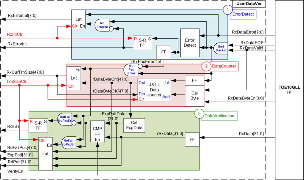
Figure 2‑9 UserDataVer block
As shown in Figure 2‑9, UserDataVer has three operations, i.e., Error detection (1) to detect the error from TOE10GLL-IP, Data counter (2) to count total number of valid data, and Data verification (3) to verify the received data.
ErrorDetect (1) reads the error output from TOE10GLL-IP (RxDataError) when the end of packet is received (RxDataEOP=’1’ and RxDataValid=’1’). If the error is detected, the interrupt flag (RxErrorInt) is asserted to ‘1’ and RxDataError is latched (RxErrorLat). After the user asserts the signal to clear interrupt (RxIntClr), the interrupt flag will be cleared.
DataCounter (2) includes the counter to count total number of receive data from TOE10GLL-IP. Valid signal of received data (RxDataValid) and byte enable (RxDataByteEn) are monitored to check the number of valid bytes in each cycle that can be equal to 1 – 4 bytes. After that, the data counter (rDataByteCnt) is increased by the amount of valid received data. To support the re-transmitted packet from error recovery process, latch register is designed to store the latest total amount of received data at the end of valid packet, named rDataByteOK. rDataByteOK is loaded to 48-bit data counter before starting receiving the new packet. Therefore, it guarantees that total data count shows the amount of valid data only. After finishing the test operation, the user can assert clear flag (TrnSizeClr) to clear the data counter before running the next test.
DataVerification (3) has CalExpData which calculates the expected data from the current data count, generated in block (2). Only 34-bit of the data count is applied. Bit[1:0] is byte offset for 32-bit expected data re-alignment while bit[33:2] is 32-bit expected data. The expected data (rExpPattData) is compared with the received data (rRxData) when the user enables the verification flag (VerifyEn). If data verification error is found and the packet is not error, Failed flag (RdFail) is asserted to ‘1’. The other signals to show verification error information, i.e., the error position in byte unit (RdFailPos), the expected value (ExpPatt), and the received value (RdPatt) are latched to show the details of the first data which is error. The error flag is cleared by asserting TrnSizeClr to ‘1’.
Asynchronous module for UserDataVer
Most logics in UserReg are run in the same clock as Tx interface of TOE10GLL-IP (MacTxClk), except UserDataVer module which is run in the same clock as Rx interface of TOE10GLL-IP (MacRxClk). Therefore, the signal interface of UserDataVer must be fed to asynchronous circuit for clock domain crossing. AsyncDataVer is the module to convert the signal from MacTxClk to MacRxClk and vice versa.
Note: TxClk of AsyncDataVer is connected to MacTxClk while RxClk is connected to MacRxClk.

Figure 2‑10 AsyncDataVer block
As shown in Figure 2‑10, there are four signal types for converting clock domain, i.e., 1-bit signal, 1-cycle pulse signal, multiple-bit signal which must be updated, and multiple-bit signal which is stable value.
Block (1) shows two Flip-flops are inserted to solve metastability problem on SigTx signal which is run on input clock domain (TxClk). The result is SigRx signal which is applied on output clock domain (RxClk). When the signal is one-bit signal and the value is valid for several cycles, block (1) is applied. The signals of UserDataVer which use block (1) circuit are VerifyEn, RdFail, and RxErrorInt.
When the one-bit signal is a pulse which is asserted to ‘1’ only one cycle, asynchronous circuit is designed as shown in block (2). First, S-R Flip flop is applied to convert the input signal (PulseTx) to be asserted to ‘1’ for several clock cycles, assigned by rPulseTx[0]. After that, the signal is forwarded to the output clock domain (RxClk) by using three Flip-flops (rPulseRx[2:0]). The pulse on the output clock domain (PulseRx) is asserted to ‘1’ for one cycle when rising edge of rPulseRx is found (rPulse[2:1]=01b). The signal on the output clock (rPulseRx[2]) is fed back to the input clock (TxClk), assigned by rPulseTx[3:1]. When detecting the rising edge of rPulseTx[3:2], it means PulseRx was asserted. After that, rPulseTx[0] is de-asserted to ‘0’ to finish the operation. The signals of UserDataVer which use block (2) circuit are RxIntClr and TrnSizeClr.
When the signal is bus type which has multiple bits and the signal is always updated, asynchronous circuit is designed as shown in block (3). Data bus must be latched on input clock domain (RxClk) to hold the same value before transferring to the output clock domain (TxClk), assigned by rBusRxLat. There is state machine which has three states for controlling clock domain crossing process, i.e., stRxUpdate - the cycle to latch input signal, stRxLat - the cycle to wait until the input signal is transferred to the output clock domain, and stRxWait - the cycle to clear the signals on input clock domain to be Idle status. The state machine is run as forever loop to always update the signal from input clock domain to output clock domain.
When state machine is in stRxUpdate, the valid signal on input clock domain (rValidRx[0]) is asserted to ‘1’ to start data updating process. Next, it is transferred to the output clock domain by using three Flip-flops, rValidToTx[2:0]. The signal is loaded to output clock domain, assigned by BusTx, when rising edge of valid signal (rValidToTx[2:1]) is detected. After that, the valid signal on the output clock domain is fed back to the input clock domain, assigned by rValidRx[2:1]. When rValidRx[2] is asserted to ‘1’, it guarantees that BusTx was updated. Therefore, state machine changes to stRxWait to de-assert rValidRx and rValidToTx to ‘0’. After all valid signal are de-asserted, state machine returns to the first state (stRxUpdate) to restart the new updated loop. The signal of UserDataVer which uses block (3) circuit is RxCurTrnSize.
The last block (4) is designed when multiple-bit signal which is stable for long time before reading the value. One Flip-flop is inserted to change clock synchronous from input clock domain (RxClk) to output clock domain (TxClk). The signals of UserDataVer which use block (4) circuit are RdFailPos, ExpPatt, and RdPatt.
2.6 Timer

Figure 2‑11 Timers in the reference design
To measure the latency time of TOE10GLL-IP for both Tx interface and Rx interface, two timers (TxTimer and RxTimer) are designed. Both timers are controlled by Start flag and Stop flag. Start flag is asserted to ‘1’ when the first data is detected at the input of the measured module. Stop flag is asserted to ‘1’ when the first data is detected at the output of the measured module. The timer latches the value for CPU reading to calculate the time in nanosecond unit for displaying on the console. Therefore, the latency time is measured by the first packet only. Other packets are ignored. The timers are rerun after the user sends the new request to transfer the data. The latency time of TOE10GLL-IP is measured from start-of-packet of the input side to start-of-packet of the output side.
3 CPU Firmware (FPGA)
In reference design, CPU firmware is implemented as bare-metal OS for easily handling with the hardware. After the test system is run, the first step in the firmware is hardware initialization.

Figure 3‑1 Message on the console during initialization process
As shown in Figure 3‑1, there are four steps to initialize the hardware, described as follows.
1) After FPGA boot-up, 10G Ethernet link up status (EMAC_STS_INTREG[0]) is polling. The CPU waits until ethernet link is established and then displays welcome message to show IP information.
2) The menu to select the initialization mode of TOE10GLL-IP is displayed. The user can set as client, server, or fixed MAC mode.
Note:
- In Client mode initialization, TOE10GLL-IP sends ARP request to get the MAC address of the target device from ARP reply. In Server mode initialization, TOE10GLL-IP waits until ARP request is received to decode MAC address and return ARP reply. In Fixed MAC mode initialization, the user needs to know MAC address of the target device because TOE10GLL-IP does not transfer ARP packet.
- When running the test environment by using one FPGA board and Test PC, it is recommended to set FPGA run as client mode.
- When the test environment uses two FPGA boards, there are three solutions to initial the connection between two boards, i.e., Client <-> Server, Client <-> Fixed MAC, and Fixed MAC <-> Fixed MAC.
3) CPU displays default value of the network parameters, i.e., initialization mode, FPGA MAC address, FPGA IP address, FPGA port number, Target IP address, and Target port number. The firmware has two default parameter sets for the operation mode. First is the parameter set for Server mode and another is the parameter set for Client/Fixed MAC mode. For Fixed MAC mode, there is an extra parameter, Target MAC address. The user can select to complete the initialization process by using default parameters or updating some parameters. The details to change the parameter are described in Reset IP menu (topic 3.2).
4) CPU waits until the IP completes the initialization process by checking if InitFinish (TOE_STS_INTREG[0]) is equal to ’1’. After that, “IP initialization complete” is displayed with the main menu. There are five test operations in the main menu. More details of each menu are described as follows.
3.1 Display parameters
This menu is designed to display the current value of all TOE10GLL-IP parameters
The step to display parameters is as follows.
1) Read the initialization mode.
2) Read all network parameters from each variable in firmware following the initialization mode, i.e., source (FPGA) MAC address, source (FPGA) IP address, source (FPGA) port number, target MAC address (only displayed in fixed MAC mode), target IP address, and target port number.
Note: The source parameters are FPGA parameters set to TOE10GLL-IP while the target parameters are the parameters of TestPC or another FPGA.
3) Print out each variable.
3.2 Reset parameters
This menu is designed to change some parameters of TOE10GLL-IP such as IP address and source port number. After setting the updated parameters to TOE10GLL-IP, the CPU resets the IP to start re-initialization process by using new parameters. Finally, the CPU waits until the initialization is completed.
The step to reset parameters is as follows.
1) Display all parameters on the console.
2) Skip to the next step if the user uses the default value. Otherwise, the menu to set all parameters is displayed.
a) Receive initialization mode from the user. If the initialization mode is changed, the latest parameter set of new mode is displayed on the console.
3) Force reset to IP by setting TOE_RST_INTREG[0]=’1’.
4) Set all parameters to TOE10GLL-IP registers such as TOE_SML_INTREG and TOE_DIP_INTREG.
5) De-assert IP reset by setting TOE_RST_INTREG[0]=’0’ to start IP initialization process. Also, UserDataGen and UserDataVer module are reset.
6) Wait until InitFinish signal (TOE_STS_INTREG[0]) is asserted to ‘1’ after finishing the initialization process.
3.3 Send data test
This menu is designed to test sending data. The user sets the parameters such as total transmit length and the open connection mode. If all inputs are valid, the port is opened. After that, 32-bit incremental test data is sent until all data is completely transferred. Finally, the port is closed in active mode.
The step to send the data is as follows.
1) Receive four parameters, i.e., transmit size, packet size, PSH flag mode, and open connection mode (active or passive) from user. After that, CPU validates all inputs. The operation is cancelled if some inputs are invalid.
2) Display recommended parameters of test application on PC by reading current parameters in the system.
3) Set UserReg parameters, i.e., transfer size (USRTX_TDL/TDH_INTREG), packet size (USRTX_PKL_INTREG), and PSH flag mode (USRTX_PSH_INTREG).
4) Send open connection command following the connection mode by setting TOE_CMD_INTREG=Active open or Passive open. After that, wait until TCPConnOn status (TOE_STS_INTREG[1]) is equal to ‘1’.
5) Set USRTX_CMD_INTREG=Send data to start sending data process by UserDataGen module. After that, wait until total transmit data size, read by USRTX_LENL/H_INTREG, is equal to set value (USRTX_TDL/H_INTREG). During transferring data, current amount of transmitted data (USRTX_LENL/H_INTREG) is displayed on console every second.
6) Set close connection command to TOE10GLL-IP register (TOE_CMD_INTREG=Active close). After that, wait until TCPConnOn status (TOE_STS_INTREG[1]) is equal to ‘0’.
7) Calculate performance and latency time, and then display a test result on the console.
3.4 Receive data test
This menu is designed to test receiving data. The user sets the parameters such as total receive length and the open connection mode. If all inputs are valid, the port is opened. After that, 32-bit incremental test data is created for verifying with the received data from PC/FPGA when the data verification is enabled.
The step to receive the data is as follows.
1) Receive three parameters, i.e., total transfer data size, data verification mode, and connection mode (active or passive) from user input. The operation is cancelled if some inputs are invalid.
2) Display recommended parameters of test application on PC by reading current parameters in the system.
3) Set UserReg parameters, data verification mode (USRRX_CMD_INTREG). Total transfer data size is stored as the variable for comparison when finishing the test.
4) Send open connection command following the connection mode by setting TOE_CMD_INTREG=Active open or Passive open. After that, wait until TCPConnOn status (TOE_STS_INTREG[1]) is equal to ‘1’.
5) Wait until TCPConnOn status (TOE_STS_INTREG[1]) is equal to ‘0’ after the target device (PC or another FPGA) closes the port when completing transferring all data. During transferring data, current amount of received data (USRRX_LENL/H_INTREG) is displayed on console every second.
6) Compare total amount of received data (USRRX_LENL/H_INTREG) with the variable, total transfer size set from the user. If they are not equal, the warning message is displayed. Next, CPU checks verification result by reading USRRX_STS_INTREG[8] (‘0’: normal, ‘1’: error) when user enables the verification. If the error is detected, the error message is displayed.
7) Calculate performance and latency time, and then display a test result on the console.
3.5 Full duplex test
This menu is designed to run full duplex test by transferring data in both directions by using the same port number at the same time. The menu receives the user parameters for running the test such as total transfer length and packet size. If all inputs are valid, the port is opened. After that, the data starts transferring. When finishing transferring data in both directions, the port is closed by the client which may be FPGA or PC The test is run as forever loop until the user cancels the operation.
Note: When running the test with PC, connection mode on FPGA must be set to passive (server operation). The transfer size on the test application, tcp_client_txrx_40G, must be equal to the transfer size set on FPGA. To stop the test operation, user presses some keys on FPGA console and then enters “Ctrl+C” on PC console consequently.
The step to run full duplex is as follows.
1) Receive five parameters, i.e., total transfer size (the same size for both directions), packet size, PSH flag mode, data verification mode, and open connection mode (active or passive) from user. The operation is cancelled if some inputs are invalid.
2) Display the recommended parameters of test application run on PC by reading current parameters in the system.
3) Send open connection command following the connection mode by setting TOE_CMD_INTREG=Active open or Passive open. After that, wait until TCPConnOn status (TOE_STS_INTREG[1]) is equal to ‘1’.
4) Set UserReg parameters, i.e., data verification mode (USRRX_CMD_INTREG), total transfer size (USRTX_TDL/TDH_INTREG), packet size (USRTX_PKL_INTREG), PSH flag mode (USRTX_PSH_REG), and command register of UserDataGen (USRTX_CMD_INTREG) to start the test operation.
5) Wait until finishing transferring all data in both directions by comparing total amount of transmitted data and received data. Total amount of transmitted data (USRTX_LENL/H_INTREG) must be equal to set value (USRTX_TDL/H_INTREG). Also, when running active connection mode, total amount of received data (USRRX_LENL/H_INTREG) must be equal to set value. During transferring data, current amount of transmitted data and received data are displayed on the console every second.
6) Set close connection following connection mode value.
a. For active close, CPU sets close command to TOE10GLL-IP register (TOE_CMD_INTREG=Active close). After that, CPU waits until TCPConnOn status (TOE_STS_INTREG[1]) is equal to ‘0’.
b. For passive close, CPU waits until TCPConnOn status (TOE_STS_INTREG[1]) is equal to ‘0’.
7) Check the result and the error (similar to Step 6 of Receive data test).
8) Calculate performance and latency time and then display a test result on the console. Return to Step 3 to repeat the test in forever loop.
3.6 Function list in User application
This topic describes the function list to run TOE10GLL-IP operation.
|
void clr_trns_status(void) |
|
|
Parameters |
None |
|
Return value |
None |
|
Description |
Set USRTX_CMD_REG[1] and USRRX_CMD_REG[1] to ‘1’ to clear USRTX_LENL/H_REG, USRTX_TMR_REG, USRRX_LENL/H_REG, and USRRX_TMR_REG. |
|
void exec_port(unsigned int port_ctl, unsigned int mode_active) |
|
|
Parameters |
port_ctl: 1-Open port, 0-Close port mode_active: 1-Active open/close, 0-Passive open/close |
|
Return value |
None |
|
Description |
Write TOE_CMD_REG to open (active or passive) or close (active) connection. After that, call read_conon function to monitor connection status until it changes from ON to OFF or OFF to ON when running close port or open port respectively. |
|
void init_param(void) |
|
|
Parameters |
None |
|
Return value |
None |
|
Description |
Reset parameters following the description in topic 3.2. In the function, show_param and input_param function are called to display parameters and get parameter from user. |
|
int input_param(void) |
|
|
Parameters |
None |
|
Return value |
0: Valid input, -1: Invalid input |
|
Description |
Receive network parameters from user, i.e., Initialization mode, FPGA MAC address, FPGA IP address, FPGA port number, Target MAC address (when running fixed MAC mode), Target IP address, and Target port number. If the input is valid, the parameter is updated. Otherwise, the value does not change. After receiving all parameters, calling show_param function do display parameters. |
|
unsigned int read_conon(void) |
|
|
Parameters |
None |
|
Return value |
0: Connection is OFF, 1: Connection is ON. |
|
Description |
Read value from TOE_STS_REG register and return only bit1 value to show connection status. |
|
void show_cursize(void) |
|
|
Parameters |
None |
|
Return value |
None |
|
Description |
Read current number of transmitted data and number of received data from global parameters (tx_cursize and rx_cursize) and then display in byte, Kbyte, or Mbyte unit |
|
void show_ipstate(void) |
|
|
Parameters |
None |
|
Return value |
None |
|
Description |
Read current state value from TOE_STS_REG[20:16] and then display the result |
|
void show_latency(void) |
|
|
Parameters |
None |
|
Return value |
None |
|
Description |
Read USRTX_TMR_REG and USRRX_TMR_REG which are latency time of transmit interface and receive interface of TOE10GLL-IP. After that, convert the unit from clock cycle to be the time in nsec. Finally, print out the value. |
|
void show_param(void) |
|
|
Parameters |
None |
|
Return value |
None |
|
Description |
Display the parameters following the description in topic 3.1. |
|
void show_recv_error(void) |
|
|
Parameters |
None |
|
Return value |
None |
|
Description |
This function is called when error is found during running receive data test. Read USRRX_ERR_REG and two errors are decoded, i.e., TCP checksum and EMAC error. |
|
void show_result(void) |
|
|
Parameters |
None |
|
Return value |
None |
|
Description |
Read total transmit data size and total receive data size from global parameters (tx_cursize and rx_cursize) and display the results. Read total time usage from global parameters (timer_val) and calculate total time usage to display in usec, msec, or sec unit. Finally, transfer performance is calculated and displayed in MB/s unit. |
|
void show_verfail(void) |
|
|
Parameters |
None |
|
Return value |
None |
|
Description |
This function is called when data verification is failed. Read USRRX_FAILPOSL/H_REG (failure position), USRRX_EXPPAT_REG (expected data), and USRRX_RDPAT_REG (received data) and print out the result on the console to show the details of the first failure data. |
|
int toe_recv_test(void) |
|
|
Parameters |
None |
|
Return value |
0: The operation is successful -1: Receive invalid input or error is found |
|
Description |
Run Receive data test following description in topic 3.4 It calls clr_trns_status, exec_port, read_conon, update_cursize, show_cursize, show_recv_error, show_verfail, show_result, and show_latency function |
|
int toe_send_test(void) |
|
|
Parameters |
None |
|
Return value |
0: The operation is successful -1: Receive invalid input or error is found |
|
Description |
Run Send data test following description in topic 3.3 It calls clr_trn_status, exec_port, read_conon, update_cursize, show_cursize, show_result, and show latency function. |
|
int toe_txrx_test(void) |
|
|
Parameters |
None |
|
Return value |
0: The operation is successful -1: Receive invalid input or error is found |
|
Description |
Run Full duplex test following described in topic 3.5 It calls clr_trns_status, exec_port, read_conon, update_cursize, show_cursize, show_recv_error, show_verfail, show_result, and show_latency function |
|
void update_cursize(void) |
|
|
Parameters |
None |
|
Return value |
None |
|
Description |
Read USRTX_LENL/H_REG and USRRX_LENL/H_REG and then update to global parameters (tx_cursize and rx_cursize). |
|
void wait_ethlink(void) |
|
|
Parameters |
None |
|
Return value |
None |
|
Description |
Read EMAC_STS_REG[0] and wait until ethernet connection is linked up |
4 Test Software on PC
4.1 “tcpdatatest” for half duplex test
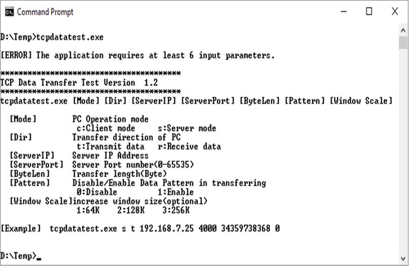
Figure 4‑1 “tcpdatatest” application usage
“tcpdatatest” is designed to run on PC for sending or receiving TCP data via Ethernet as Server or Client mode. It is recommended to run PC in the demo by using Client mode. There are six parameters which must be set by the user before running the application, described as follows.
1) Mode: c –PC runs in Client mode and FPGA runs in Server mode (recommended)
2) Dir : t – transmit mode (PC sends data to FPGA)
r – receive mode (PC receives data from FPGA)
3) ServerIP : IP address of FPGA when PC runs in Client mode (default is 192.168.7.42)
4) ServerPort: Port number of FPGA when PC runs in Client mode (default is 4000)
5) ByteLen : Total transfer size in byte unit. This input is used in transmit mode only and ignored in receive mode. In receive mode, the application is closed when the connection is terminated. In transmit mode, ByteLen must be equal to total transfer size on FPGA, set in receive data test menu.
6) Pattern:
0 – Generate dummy data in transmit mode or disable data verification in receive mode.
1 – Generate incremental data in transmit mode or enable data verification in receive mode.
Note: Window Scale: Optional parameter which is not used in the demo.
Transmit data mode
Following sequence is the sequence when test application runs in transmit mode.
1) Get parameters from the user and verify that the input is valid.
2) Create the socket and set socket options.
3) Create the new connection by using server IP address and server port number.
4) Allocate 1 MB memory to be send buffer.
5) Skip this step if the dummy pattern is selected. Otherwise, generate the incremental test pattern to send buffer.
6) Send data out and read total number of sent data from the function.
7) Calculate remaining transfer size.
8) Print current transmit data size every second.
9) Repeat step 5) – 8) until the remaining transfer size is 0.
10) Calculate transfer performance and print the result on the console.
11) Close the socket and free the memory.
Receive data mode
Following sequence is the sequence when test application runs in receive mode.
1) Follow the step 1) – 3) of Transmit data mode.
2) Allocate memory to be receive buffer.
3) Read data from the receive buffer and calculate total receive size.
4) This step is skipped if data verification is disabled. Otherwise, received data is verified by the incremental pattern. Error message is printed out when data is not correct.
5) Print current receive data size every second.
6) Repeat step 3) – 5) until the connection is closed.
7) Calculate transfer performance and print the result on the console.
8) Close socket and free the memory.
4.2 “tcp_client_txrx_40G” for full duplex test
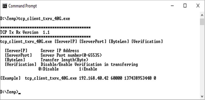
Figure 4‑2 “tcp_client_txrx_40G” application usage
“tcp_client_txrx_40G” application is designed to run on PC for sending and receiving TCP data through Ethernet by using the same port number at the same time. The application is run in Client mode. Therefore, the server parameters are the network parameters of TOE10GLL-IP. As shown in Figure 4‑2, there are four parameters to run the application, described as follows.
1) ServerIP : IP address of FPGA
2) ServerPort : Port number of FPGA
3) ByteLen : Total transfer size in byte unit. This is total number of transmitted data and received data. This value must be equal to the transfer size set on FPGA for running full-duplex test.
4) Verification :
0 – Generate dummy data for sending function and disable data verification for receiving function. When running this mode, it shows the best performance of full-duplex transfer.
1 – Generate incremental data for sending function and enable data verification for receiving function.
The sequence of test application is as follows.
(1) Get parameters from the user and verify that the input is valid.
(2) Create the socket and set socket options.
(3) Create the new connection by using server IP address and server port number.
(4) Allocate 64 KB memory for send buffer and receive buffer.
(5) Generate incremental test pattern to send buffer when the test pattern is enabled. Skip this step if dummy pattern is selected.
(6) Send data out, read total sent data from the function, and calculate remaining send size.
(7) Read data from the receive buffer and calculate total receive data size.
(8) Skip this step if data verification is disabled. Otherwise, data is verified by incremental pattern. Error message is printed out when data is not correct.
(9) Print current send data size and current receive data size every second.
(10)Repeat step 5) – 9) until total number of send size and total number of receive size are equal to ByteLen, set by user.
(11)Calculate transfer performance and print the result on the console.
(12)Close the socket.
(13)Sleep for 1 second to wait until the hardware completes the current test loop.
(14)Run step 3) – 13) in forever loop. If verification is failed, the application is stopped.
5 Revision History
|
Revision |
Date |
Description |
|
1.2 |
21-Apr-22 |
- Update UserDataGen module - Update Register map |
|
1.1 |
5-May-21 |
Change Xilinx Transceiver mode to be Raw |
|
1.0 |
18-Nov-20 |
Initial version release |