exFAT2 IP for Gen4 reference design manual
3.1 Test firmware (exfat2g4test.c)
3.2 Function list in Test firmware
1 Introduction
To store data stream on an NVMe SSD, a high-performance storage solution, users must decide between two data formats: raw data format or file system format. In the raw data format, data indices use the physical address of SSD, and users are responsible for managing data structure themselves, especially when dealing with various data types stored on the SSD. Implementing a customized data structure requires dedicated human resources for development and maintenance, especially when integrating with multiple host systems accessing the SSD. However, this approach offers the best performance for data transfer with the SSD.
On the other hand, standard file systems like FAT32 and exFAT provide a comprehensive solution for treating each piece of data as a �file�. These file systems are well-designed, utilizing file entries to denote file names, types, sizes, and data allocations. FAT32 and exFAT file systems have been widely implemented by various developers, enabling users to integrate standard libraries into their host systems for accessing files on the SSD. However, this convenience comes at the cost of CPU or processor resources required to manage file entries and file data, which can result in constrained write/read performance during file data access.
To overcome the performance constraints associated with using file system, Design Gateway offers IP cores that implements the FAT32 and exFAT file systems using pure hardware logics, called FAT32 IP and exFAT2 IP. This approach ensures maximum transfer performance for data transfers with SSD, similar to the raw data format. Further information of FAT32 IP can be found from following site.
https://dgway.com/products/IP/NVMe-IP/dg_fat32ip_nvme_data_sheet_en/
Compared to the FAT32 file system, the exFAT file system offers several improvements. Firstly, exFAT supports file size larger than 4 GB and disk capacities exceeding 2 TB. Additionally, it implements name hashing for file names to enhance search functionality and employs checksums in the system data area to boost data reliability. However, exFAT demands much host resources for managing file systems and some legacy systems support only the FAT32 file system, not exFAT.
The exFAT2-IP is an IP core designed to directly interface with the (mu)NVMe IP, an NVMe host controller IP core from Design Gateway. It achieves the same performance as using the raw data format under PCIe Gen4 speed, with read access reaching up to 7500 MB/s. Figure 1‑1 illustrates the block diagram of the reference design, showcasing the comparison between the raw data access without the exFAT2-IP and the file system access using the exFAT2-IP.
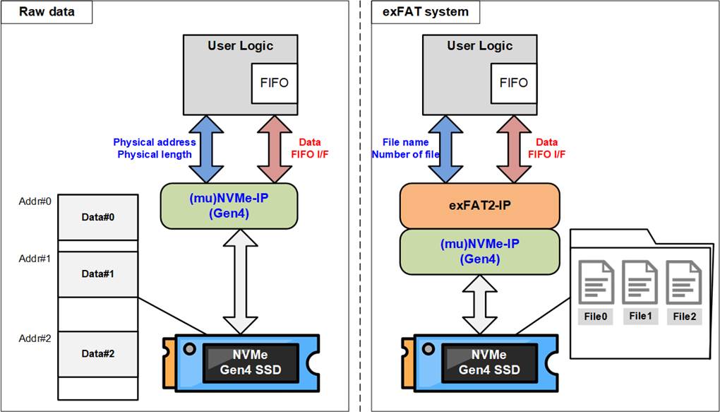
Figure 1‑1 Hardware system using (mu)NVMe-IP for raw data and file system
As shown on the left side of Figure 1‑1, when utilizing the (mu)NVMe-IP to access an NVMe SSD, the stored data is in raw data format, accessed via physical address. Consequently, the input parameters assigned to the (mu)NVMe-IP consist of physical address and transfer length measured in 512-byte units.
In contrast, on the right side of Figure 1‑1, with the exFAT2-IP inserted between the user logic and the (mu)NVMe-IP for accessing an NVMe SSD, the data stored on the SSD adopts the exFAT file system format, denoted as File0, File1, and File2. The input parameters designated for the exFAT2-IP include file names and the number of files, which are subsequently computed into physical address and 512-byte transfer length supplied to the (mu)NVMe-IP.
Both the raw data system and exFAT file system utilize FIFO interfaces for their data interfaces.
The exFAT2-IP can interface with the NVMe-IP for a single user interface or the muNVMe-IP for multiple user interfaces, as illustrated in Figure 1‑2.
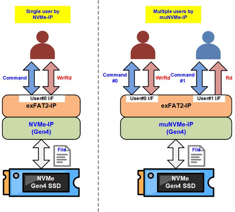
Figure 1‑2 Hardware comparison between single user and multiple users
For a single user system, the exFAT2-IP interfaces with the NVMe-IP via channel#0, supporting six commands: Format, Secure Format, Shutdown, Write file, Read file, and Read file info. In multiple-user system, the exFAT2-IP connects to the muNVMe-IP, offering both User#0 I/F and User#1 I/F. While User#0 supports all six commands, User#1 is limited to two commands: Read file and Read file info.
2 Hardware overview
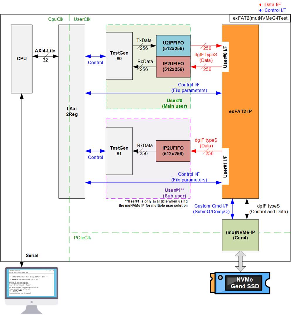
Figure 2‑1 exFAT2-IP reference design
The reference design of the exFAT2-IP has been adapted from the base reference design of the (mu)NVMe-IP for Gen4 reference design by integrating the exFAT2-IP between the user module and the (mu)NVMe-IP. Additionally, the Test logic has been modified to change the input parameters from the physical index of the SSD to file index. Consequently, the CPU firmware has also been updated to adjust parameter names and include the additional information about the file system, such as created date and created time. For further details about the (mu)NVMe-IP base reference design, please refer to the following links.
Single-user system: NVMe-IP (Gen4) reference design document
https://dgway.com/products/IP/NVMe-IP/dg_nvmeip_refdesign_g4_en/
Multiple-user system: muNVMe-IP (Gen4) reference design document
https://dgway.com/products/IP/NVMe-IP/dg_munvmeip_refdesign_g4_xilinx/
When employing an NVMe-IP for a single-user system, the reference design integrates only User#0 to enable users to execute all six commands: Format, Secure Format, Write file, Read file, Read file info, and Shutdown. Users can configure the maximum data speed of User#0 while executing Write file and Read file commands.
In contrast, when utilizing a muNVMe-IP for a multiple-user system, User#1 is included to enable users to execute Read file and Read file info commands. As a result, TestGen#1 within User#1 contains only a Read data interface.
The same CPU firmware is designed for both single-user and multiple-user systems, with the number of users being configurable within the firmware.
Further details of each submodule in the exFAT2-IP reference design are described below.
2.1 TestGen
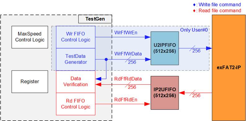
Figure 2‑2 TestGen interface
Each TestGen module manages the data interface for each user of the exFAT2-IP, facilitating data transfer in both directions. However, since the User#1 I/F of the exFAT2-IP does not support the Write file command, the write interface logic is not available in User#1.
During a Write file command, TestGen sends 256-bit test data to the exFAT2-IP. In contrast, during a Read file command, the test data is received for comparison with the expected value, ensuring data accuracy.
Within this block, there is a MaxSpeed Control Logic that generates an enable pulse to regulate the number of clock cycles in which 1b is asserted out of every 100 clock cycles. This enable pulse is then fed to both the Wr FIFO and Rd FIFO Control Logics, enabling control over the maximum data rate of Write/Read data transfers. The Wr FIFO and Rd FIFO Control Logics assert the write enable and read enable signals when the FIFO is ready, and the enable pulse from the MaxSpeed Control Logic is activated.
The Register file in the TestGen receives various test parameters from the user, including file name, file size, the number of files, transfer direction, verification enable, test pattern selector, and transfer rate. For further details of the hardware logic of TestGen, refer to Figure 2‑3.
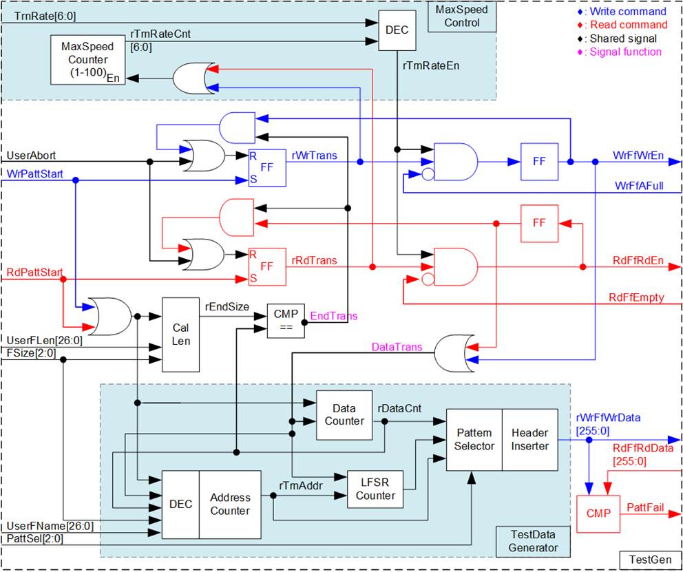
Figure 2‑3 TestGen hardware
The MaxSpeed Control Logic utilizes a counter named MaxSpeed Counter along with a decoder to assert rTrnRateEn to 1b. The TrnRate input specifies the number of cycles which rTrnRateEn is asserted to 1b out of every 100 clock cycles. This counter operates when either a Write file or Read file command is in progress (rWrTrans=1b or rRdTrans=1b). By monitoring rTrnRateCnt, rTrnRateEn can be asserted to 1b or de-asserted to 0b at specific times to control the maximum data rate. The Write and Read FIFO enable signals are only asserted when rTrnRateEn is set to 1b.
Note: If the abort function is enabled in this reference design, using the customized (mu)NVMe-IP, the assertion of UserAbort can de-assert WrFfWrEn and RdFfRdEn to 0b, similar to the end transfer condition.
The �TestData Generator� subblock is responsible for generating the test data (WrData) that will be transmitted to the exFAT2-IP during the Write file command. Each 512-byte data segment comprises a 64-bit header data and a test pattern, selected by the PattSel parameter.
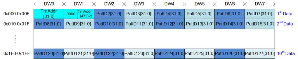
Figure 2‑4 Test pattern format in each 512-byte data for Increment/Decrement/LFSR pattern
As shown in Figure 2‑4, the 64-bit header at DW#0 (Dword#0) and DW#1 is generated by combining the 48-bit signal of rTrnAddr, computed from UserFName and FSize, with a zero value. The remaining data (DW#2 � DW#1023) represents the test pattern, which can be chosen from three different formats: 32-bit incremental data, 32-bit decremental data, and 32-bit LFSR counter. The 32-bit incremental data is derived from the output of the Data Counter. The decremental data is obtained by applying the logical NOT operation to the incremental data. The LFSR data is generated using the Fibonacci LFSR algorithm, following the equation x^31 + x^21 + x + 1.
To implement the 256-bit LFSR pattern, the data is divided into two sets of 128-bit data, each having a distinct initial value. The 128-bit data employs a look-ahead technique to calculate four 32-bit LFSR data in one clock cycle. As illustrated in Figure 2‑5, the initial value of the LFSR is determined by combining a portion of the lower 32 bits of TrnAddr signal with the logical NOT of the lower 32 bits of TrnAddr signal (TrnAddrB).
In case of the all-zero and all-one patterns, a 64-bit header is not included within the 512-byte data. These patterns are often used to assess the optimal Write/Read performance of certain SSDs.
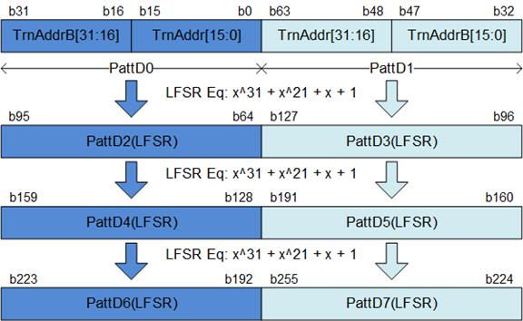
Figure 2‑5 256-bit LFSR Pattern in TestGen
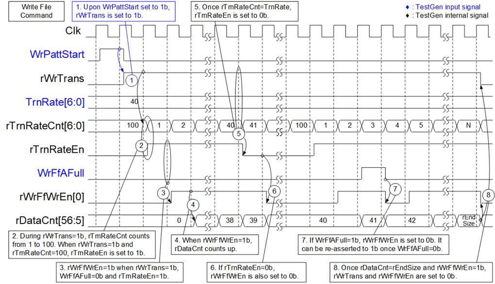
Figure 2‑6 Timing diagram of Write file operation in TestGen
1) The operation begins when WrPattStart is asserted to 1b. This signal remains asserted for only one clock cycle. Subsequently, rWrTrans is set to 1b, indicating that Write request is in progress. It is de-asserted upon completion of the operation or reception of abort.
2) While rWrTrans is set to 1b, rTrnRateCnt counts up from 1 to 100. The initial value of rTrnRateCnt is 100. When rWrTrans=1b and rTrnRateCnt=100, rTrnRateEn is asserted to 1b.
3) When both rWrTrans and rTrnRateEn are asserted to 1b, and the FIFO is not full (WrFfAFull=0b), rWrFfWrEn is asserted to 1b, allowing the test data to be written to FIFO.
4) The data counter (rDataCnt) increments when rWrFfWrEn is asserted to 1b. Therefore, it can be monitored to determine the total amount of data transmitted to the FIFO.
5) In this example, TrnRate is set to 40, resulting in a maximum data rate of approximately 40/100 = 40% of the logic�s maximum throughput. rTrnRateEn is asserted to 1b for 40 cycles out of every 100 cycles. Once rTrnRateCnt=40, rTrnRateEn is de-asserted to 0b.
6) When rTrnRateEn is de-asserted to 0b, rWrFfWrEn is also de-asserted to 0b, temporarily pausing the transmission of data.
7) If the FIFO becomes full (WrFfAFull=1b), the writing process is paused by de-asserting rWrFfWrEn to 0b. rWrFfWrEn is re-asserted to 1b when WrFfAFull is de-asserted to 0b.
8) Once the total data count (rDataCnt) equals to the total transfer size (rEndSize), both rWrTrans and rWrFfWrEn are de-asserted to 0b, indicating the completion of the Write file command.
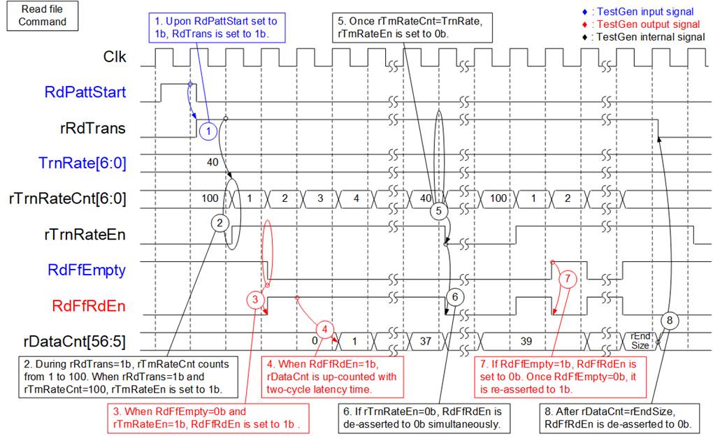
Figure 2‑7 Timing diagram of Read file operation in TestGen
1) The operation begins when RdPattStart is asserted to 1b. This signal remains asserted for only one clock cycle. Subsequently, rRdTrans is asserted to 1b to control rTrnRateEn It is de-asserted once all data has been completely transferred or the abort has been requested.
2) While rRdTrans is set to 1b, rTrnRateCnt increments from 1 to 100. The initial value of rTrnRateCnt is 100. If rRdTrans=1b and rTrnRateCnt=100, rTrnRateEn is asserted to 1b.
3) When rTrnRateEn is asserted to 1b and the FIFO contains data (RdFfEmpty=0b), RdFfRdEn is asserted to 1b, enabling the reading of test data from the FIFO.
4) The data counter (rDataCnt) increments after RdFfRdEn is asserted to 1b for two clock cycles. It can be monitored to determine the total amount of received data from the FIFO.
5) In this example, TrnRate is set to 40, resulting in a maximum data rate of approximately 40/100 = 40% of the logic�s maximum throughput. rTrnRateEn is asserted to 1b for 40 cycles out of every 100 cycles. Once rTrnRateCnt=40, rTrnRateEn is de-asserted to 0b.
6) If rTrnRateEn is de-asserted to 0b, RdFfRdEn is also de-asserted to 0b, pausing the transmission of data in the same clock cycle.
7) If the FIFO becomes empty (RdFfEmpty=1b), the reading process is paused by de-asserting RdFfRdEn to 0b. RdFfRdEn is re-asserted to 1b when RdFfEmpty is de-asserted to 0b.
8) Once the total data count (rDataCnt) equals the total transfer size (rEndSize), rRdTrans is de-asserted to 0b, indicating the completion of the Read file command.
2.2 exFAT
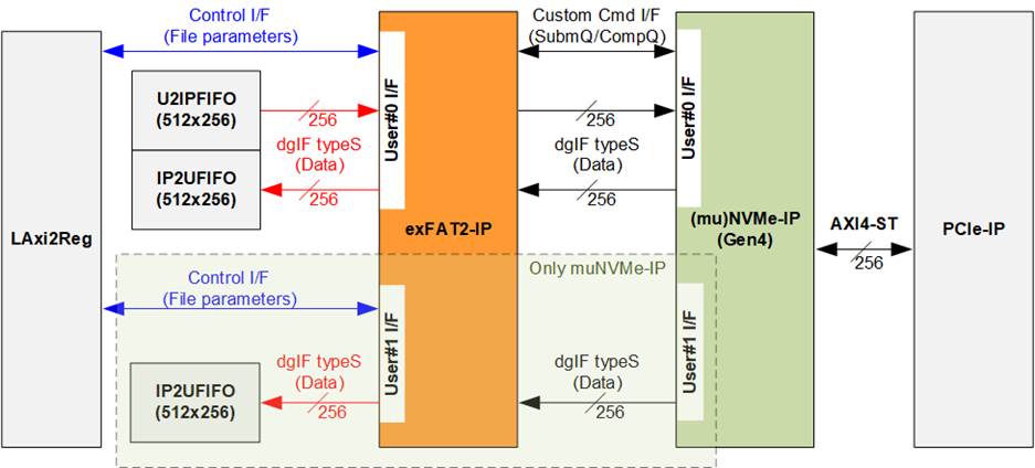
Figure 2‑8 exFAT hardware
An exFAT hardware set contains three submodules: the exFAT2-IP, the (mu)NVMe-IP, and the PCIe-IP. The user logic is designed to connect with the exFAT2-IP, which provides two interface types: the Control interface and the Data interface. In this reference design, the Control interface is connected to LAxi2Reg, while the Data interface is connected to the FIFOs. For a single-user design, only User#0 is available, utilizing the NVMe-IP. For a multiple-user design, both User#0 and User#1 are available, utilizing the muNVMe-IP. Further details of each submodule are described in this section.
2.2.1 exFAT2-IP
The exFAT2-IP is an extension module of the (mu)NVMe-IP, an IP core from Design Gateway, designed to store and retrieve data on the NVMe SSD using the exFAT file system instead of the raw data format, while achieving the same performance as the raw data format. It supports both single-user and multiple-user interfaces, depending on the NVMe-IP model (muNVMe-IP or NVMe-IP). Additionally, the exFAT2-IP supports an abort function if the selected NVMe-IP is the customized version that enables the Abort function. Further details of the exFAT2-IP can be found in the datasheet available on our website.
https://dgway.com/NVMe-IP_X_E.html
2.2.2 (mu)NVMe-IP for Gen4
Design Gateway provides several NVMe-IP solutions for accessing an NVMe Gen4 SSD. Two main categories are a single user interface using NVMe-IP and multiple-user interface using muNVMe-IP. Each category has its sub-category for using the PCIe hard IP or the PCIe soft IP. Please contact our sales for further information. The lists of our NVMe-IP solutions for NVMe Gen4 SSD are as follows.
NVMe-IP (Gen4) using PCIe hard IP
https://dgway.com/products/IP/NVMe-IP/dg_nvme_ip_data_sheet_g4_en/
NVMe-IP with PCIe Gen4 Soft IP using PCIe PHY IP
https://dgway.com/products/IP/NVMe-IP/dg_nvmeg4_ip_data_sheet_xilinx_en/
muNVMe-IP (Gen4) using PCIe hard IP
https://dgway.com/products/IP/NVMe-IP/dg_munvme_ip_data_sheet_g4_xilinx/
2.2.3 PCIe-IP
The type of PCIe-IP used for collaboration with each NVMe-IP model may vary, including Integrated Block for PCIe (PCIe hard IP) or PCIe PHY. The details of each PCIe-IP type are described below.
a) Integrated Block for PCIe
This block refers to the hard IP integrated into certain AMD Xilinx FPGAs to support PCIe Gen4 speed. It encompasses the Physical, Data Link, and Transaction Layers of the PCIe specification. More detailed information can be found in the AMD Xilinx documents.
PG213: UltraScale+ Devices Integrated Block for PCI Express
https://www.xilinx.com/products/intellectual-property/pcie4-ultrascale-plus.html#documentation
PG343: Versal ACAP Integrated Block for PCI Express
https://www.xilinx.com/products/intellectual-property/pcie-versal.html#documentation
The PCIe hard IP is generated using the IP wizard. It is recommended for users to select a �PCIe Block Location� that is in close proximity to the transceiver pin connecting to the SSD. Further details regarding the location of the PCIe hard IP and the transceiver can be found in the following documents.
UG575: UltraScale and UltraScale+ FPGAs Packaging and Pinouts
https://www.xilinx.com/support/documentation/user_guides/ug575-ultrascale-pkg-pinout.pdf
AM013: Versal ACAP Packaging and Pinouts
https://www.xilinx.com/support/documentation/architecture-manuals/am013-versal-pkg-pinout.pdf
An example of the PCIe hard IP location on the XCVC1902-VSVA2197 is shown in Figure 2‑9.
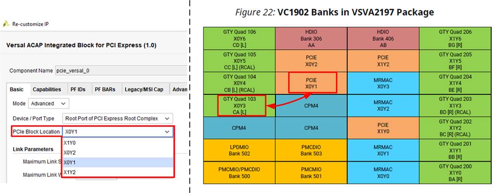
Figure 2‑9 PCIe Hard IP Pin location
b) PCIe PHY
The PCIe PHY is provided by AMD Xilinx to enable the utilization of Soft IP instead of Hard IP to construct a PCIe MAC. The PCIe PHY utilizes the PHY Interface for PCIe Express (PIPE) as its user interface. To operate with the NVMeG4-IP, it is configured to 4-lane, with each lane operating at 16.0 GT/s. For more detailed information of the PCIe PHY, please refer to the �PG239: PCI Express PHY� document, available at Xilinx website.
https://docs.xilinx.com/r/en-US/pg239-pcie-phy
2.3 CPU and Peripherals
The CPU system uses a 32-bit AXI4-Lite bus as the interface to access peripherals such as the Timer and UART. The system also integrates an additional peripheral to access the test logic by assigning a unique base address and address range. To support CPU read and write operations, the hardware logic must comply with the AXI4-Lite bus standard. LAxi2Reg module, as shown in Figure 2‑10, is designed to connect the CPU system via the AXI4-Lite interface, in compliance with the standard.
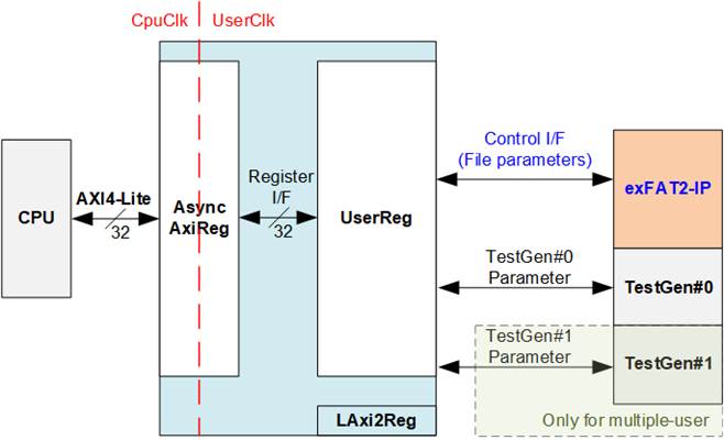
Figure 2‑10 CPU and peripherals hardware
UserReg includes the register file of parameters and the status signals of other modules in the test system, including the exFAT2-IP and TestGen. More details of AsyncAxiReg and UserReg are explained below.
2.3.1 AsyncAxiReg
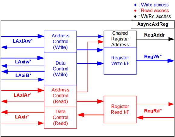
Figure 2‑11 AsyncAxiReg Interface
According to the AXI4-Lite standard, the write channel and read channel operate independently for both control and data interfaces. Therefore, the logic in the AsyncAxiReg module to interface with the AXI4-Lite bus is divided into four groups: Write control logic, Write data logic, Read control logic, and Read data logic, as shown on the left side of Figure 2‑11. The Write control I/F and Write data I/F of the AXI4-Lite bus are latched and transferred to become the Write register interface with clock domain crossing registers. Similarly, the Read control I/F of the AXI4-Lite bus is latched and transferred to the Read register interface, while Read data is returned from the Register interface to the AXI4-Lite bus via clock domain crossing registers. In the Register interface, RegAddr is a shared signal for write and read access, loading the value from LAxiAw for write access or LAxiAr for read access.
The Register interface is compatible with a single-port RAM interface for write transaction. However, the read transaction of the Register interface has been slightly modified from the RAM interface by adding the RdReq and RdValid signals to control read latency time. Since the address of the Register interface is shared for both write and read transactions, the user cannot write and read the register simultaneously. The timing diagram of the Register interface is shown in Figure 2‑12.
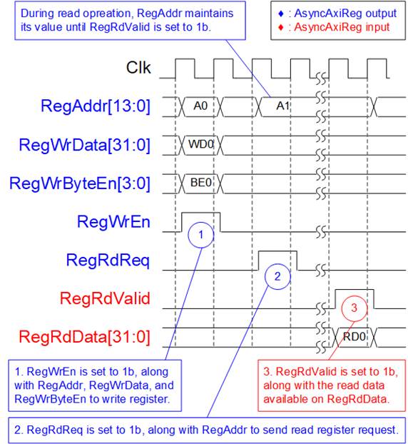
Figure 2‑12 Register interface timing diagram
1) Timing diagram to write register is similar to that of a single-port RAM. The RegWrEn signal is set to 1b, along with a valid RegAddr (Register address in 32-bit units), RegWrData (write data for the register), and RegWrByteEn (write byte enable). The byte enable consists of four bits that indicate the validity of the byte data. For example, bit[0], [1], [2], and [3] are set to 1b when RegWrData[7:0], [15:8], [23:16], and [31:24] are valid, respectively.
2) To read register, AsyncAxiReg sets the RegRdReq signal to 1b with a valid value for RegAddr. The 32-bit data is returned after the read request is received. The slave detects the RegRdReq signal being set to start the read transaction. In the read operation, the address value (RegAddr) remains unchanged until RegRdValid is set to 1b. The address can then be used to select the returned data using multiple layers of multiplexers.
3) The slave returns the read data on RegRdData bus by setting the RegRdValid signal to 1b. After that, AsyncAxiReg forwards the read value to the LAxir* interface.
2.3.2 UserReg
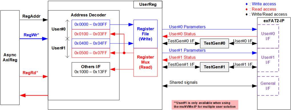
Figure 2‑13 UserReg Interface
The UserReg module consists of an Address decoder, a Register File, and a Register Mux. The Address decoder interprets the address requested by AsyncAxiReg and selects the active register for either write or read transactions. The address range assigned in UserReg is divided into three areas, as illustrated in Figure 2‑13.
1) 0x0000 � 0x03FF: mapped to User#0 of exFAT2-IP, TestGen#0, and status of exFAT2-IP.
2) 0x0400 � 0x07FF: mapped to User#1 of exFAT2-IP and TestGen#1.
3) 0x1000 � 0x13FF: mapped to other interfaces such as IP versions of exFAT2-IP and (mu)NVMe-IP.
For reading a register, multi-level multiplexers (mux) select the data to return to the CPU, using the address. The lower bits of RegAddr are fed to the submodule to choose the active data inside it, while the upper bits are used in UserReg to select the active submodule to retrieve read data. The total latency time of read data is equal to three clock cycles, and RegRdValid is created by RegRdReq by asserting three D Flip-flops. Further details of the address mapping within the UserReg module are shown in Table 2‑1.
Table 2‑1 Register Map for exFAT2-IP reference design
|
Address |
Register Name |
Description |
|
Rd/Wr |
(Label in the �exfat2g4test.c�) |
|
|
0x0000 � 0x03FF: Signal Interface of User#0 (exFAT2-IP) and TestGen#0 |
||
|
0x0000 � 0x00FF: Control signals of exFAT2-IP, User#0, and TestGen#0 (Write access only) |
||
|
BA+0x0000 |
User#0 File Name Reg |
[26:0]: Input to U0FName of exFAT2-IP, the first file name to execute commands. |
|
(U0FNAME_INTREG) |
||
|
BA+0x0004 |
User#0 File Length Reg |
[26:0]: Input to U0FLen of exFAT2-IP, the total number of files requested in this command. |
|
(U0FLEN_INTREG) |
||
|
BA+0x0008 |
User#0 Command Reg |
[2:0]: Input to U0Cmd of exFAT2-IP, commands. 000b: Format, 001b: Shutdown, 010b: Write file, 011b: Read file, 100b: Secure Format, 101b: Read file info [8]: Input to U0Req of exFAT2-IP, command request. [9]: Input to U0Abort of exFAT2-IP, abort request. |
|
(U0CMD_INTREG) |
||
|
BA+0x000C |
User#0 Test Pattern Reg |
[2:0]: Select test data pattern of TestGen#0 000b-Increment, 001b-Decrement, 010b-All 0, 011b-All 1,100b-LFSR |
|
(U0PATTSEL_INTREG) |
||
|
BA+0x0010 |
User#0 Transfer Rate Reg |
[6:0]: Transfer rate in percentage unit of TestGen#0. It is valid from 1 � 100. For example, when set to a value of 40, the maximum data rate equal 40% of the maximum data rate, which is 275 MHz x 256 bits (8.8 GB/s), equivalent to 3520 MB/s. |
|
(U0TRNRATE_INTREG) |
||
|
BA+0x0014 |
User#0 Fifo Reset Reg |
[0]: Reset flag for U2IPFIFO and IP2UFIFO of User#0. Set to 1b to assert a reset and then clear to 0b to de-assert a reset and initiate the test operation. |
|
(U0RSTFIFO_INTREG) |
||
|
BA+0x0020 |
User#0 File Size Reg |
[3:0]: Input to U0FSize of exFAT2-IP, configured file size. |
|
(U0FSIZE_INTREG) |
||
|
BA+0x0024 |
User#0 Created Date and Time Reg |
[4:0]: Input to U0FTimeS of exFAT2-IP, second multiplied by 2. [10:5]: Input to U0FTimeM of exFAT2-IP, minute. [15:11]: Input to U0FTimeH of exFAT2-IP, hour. [20:16]: Input to U0FDateD of exFAT2-IP, date. [24:21]: Input to U0FDateM of exFAT2-IP, month. [31:25]: Input to U0FDateY of exFAT2-IP, year. |
|
(U0DATETIME_INTREG) |
||
|
0x0100 � 0x03FF: Status signals of exFAT2-IP, User#0, and TestGen#0 (Read access only) |
||
|
BA+0x0100 |
User#0 Status Reg |
[0]: Mapped to U0Busy of exFAT2-IP, busy status. [1]: Mapped to U0Error of exFAT2-IP, error flag. [2]: Data verification fail in TestGen#0 (0b: Normal, 1b: Fail). |
|
(U0STS_INTREG) |
||
|
BA+0x0104 |
User#0 Error Type Reg |
[7:0]: Mapped to U0ErrorType[7:0] of exFAT2-IP, indicating error status of exFAT2-IP. |
|
(U0ERRTYPE_INTREG) |
||
|
BA+0x0108 |
User#0 NVMe Error Type Reg |
[31:0]: Mapped to U0NVMeErrorType[31:0] of exFAT2-IP, indicating error status of (mu)NVMe-IP. |
|
(U0NVMERRTYPE_INTREG) |
||
|
BA+0x0110 |
User#0 File Info Reg |
[31:0]: Mapped to U0FInfo of exFAT2-IP, modified date and time of file. |
|
(U0FINFO_INTREG) |
||
|
BA+0x0120 |
User#0 Test Pin (Low) Reg |
[31:0]: Mapped to U0TestPin[31:0] of exFAT2-IP, reserved for internal use. |
|
(U0TESTPINL_INTREG) |
||
|
BA+0x0124 |
User#0 Test Pin (High) Reg |
[63:32]: Mapped to U0TestPin[63:0] of exFAT2-IP, reserved for internal use. |
|
(U0TESTPINH_INTREG) |
||
|
BA+0x0128 |
User#0 NVMe Test pin (Low) Reg |
[31:0]: Mapped to U0TestPin[31:0] of muNVMe-IP or TestPin[31:0] of NVMe-IP, reserved for internal use. |
|
(U0NVMTESTPINL_INTREG) |
||
|
BA+0x012C |
NVMe User#0 Test pin (High) Reg |
[47:32]: Mapped to U0TestPin[47:32] of muNVMe-IP. |
|
(NVMU0TESTPINH_INTREG) |
||
|
BA+0x0140 |
Total File Capacity Reg |
[26:0]: Mapped to TotalFCap[26:0] of exFAT2-IP, maximum number of files for this SSD. |
|
(TOTALFCAP_INTREG) |
||
|
BA+0x0144 |
Directory Capacity Reg |
[19:0]: Mapped to DirCap[19:0] of exFAT2-IP, maximum number of files for each directory. |
|
(DIRCAP_INTREG) |
||
|
Address |
Register Name |
Description |
|
Rd/Wr |
(Label in the �exfat2g4test.c�) |
|
|
0x0000 � 0x03FF: Signals Interface of User#0 (exFAT2-IP) and TestGen#0 |
||
|
0x0100 � 0x03FF: Status signals of exFAT2-IP, User#0, and TestGen#0 (Read access only) |
||
|
BA+0x0148 |
Disk File Size Reg |
[3:0]: Mapped to DiskFsize of exFAT2-IP, file size currently used in this SSD. |
|
(DFSIZE_INTREG) |
||
|
BA+0x014C |
Total Count of Files in the Disk Reg |
[26:0]: Mapped to DiskFnum of exFAT2-IP, total count of files in the SSD. |
|
(DFNUM_INTREG) |
||
|
BA+0x0150 |
Current Total Count of Files in the Disk Reg |
[26:0]: Mapped to DiskFnumCur of exFAT2-IP, current total count of files in the SSD which is available only when using multiple-user. |
|
(DFNUMCUR_INTREG) |
||
|
BA+0x0160 |
NVMe LBA Size (Low) Reg |
[31:0]: Mapped to LBASize[31:0] of (mu)NVMe-IP, total capacity of SSD in 512-byte unit. |
|
(NVMLBASIZEL_INTREG) |
||
|
BA+0x0164 |
NVMe LBA Size (High) Reg |
[15:0]: Mapped to LBASize[47:32] of (mu)NVMe-IP, total capacity of SSD in 512-byte unit. [30]: Mapped to SuppSecureFmt of exFAT2-IP, Secure Format supported flag. [31]: Mapped to LBAMode of (mu)NVMe-IP, indicating LBA unit size of SSD. |
|
(NVMLBASIZEH_INTREG) |
||
|
BA+0x0168 |
User#0 NVMe Completion Status Reg |
Completion Status from (mu)NVMe-IP [15:0]: Mapped to U0AdmCompStatus[15:0] or AdmCompStatus[15:0]. [31:16]: Mapped to U0IOCompStatus[15:0] or IOCompStatus[15:0]. |
|
(NVMCOMPSTS_INTREG) |
||
|
BA+0x016C |
NVMe CAP Reg |
[31:0]: Mapped to NVMeCAPReg[31:0] of (mu)NVMe-IP, capabilities of NVMe. |
|
(NVMCAP_INTREG) |
||
|
BA+0x0180 � BA+0x018F |
NVMe MAC Test pin 0-3 Reg |
Mapped to MACTestPin[127:0] of NVMeG4-IP (NVMe IP with PCIe Gen4 Soft IP), not available for other IP models. 0x0180: Bits[31:0], 0x0184: Bits[63:32], 0x0188: Bits[95:64], 0x018C: Bits[127:96] |
|
NVMMACTESTPIN0-3 _INTREG |
||
|
BA+0x01A0 |
User#0 Abort Write File Name Reg |
[26:0]: Mapped to U0AbortFName[26:0] of exFAT2-IP, indicating the last written file name. |
|
(U0ABTFNAME_INTREG) |
||
|
BA+0x01A4 |
User#0 Abort Current Write Length Reg |
[25:0] Mapped to U0AbortCurWrLen[25:0] of exFAT2-IP, indicating completely written data size of the last file. |
|
(U0ABTCURWRLEN_INTREG) |
||
|
BA+0x0200 |
User#0 Current Test Data in Bytes (Low) Reg |
[31:0]: Bits[31:0] of the current data transfer size in bytes of TestGen#0 module when operating Write file or Read file command. |
|
(U0CURTESTSIZEL_INTREG) |
||
|
BA+0x0204 |
User#0 Current Test Data in Bytes (High) Reg |
[24:0]: Bits[56:32] of the current data transfer size in bytes of TestGen#0 module when operating Write file or Read file command. |
|
(U0CURTESTSIZEH_INTREG) |
||
|
BA+0x0210 |
User#0 Failure Byte Address (Low) Reg |
[31:0]: Bits[31:0] of the byte address in the file at the 1st failure data in TestGen#0 when operating Read file command. |
|
(U0FAILADDRL_INTREG) |
||
|
BA+0x0214 |
User#0 Failure Byte Address (High) Reg |
[6:0]: Bits[38:32] of the byte address in the file at the 1st failure data in TestGen#0 when operating Read file command. |
|
(U0FAILADDRH_INTREG) |
||
|
BA+0x0218 |
User#0 Failure File Name Reg |
[26:0]: Filename of the 1st failure data in TestGen#0 when operating Read file command. |
|
(U0FAILFNAME_INTREG) |
||
|
BA+0x0280� BA+0x029F |
User#0 Expected value Word0-7 Reg |
256-bit of the expected data at the 1st failure data in TestGen#0 when operating Read file command 0x0280: Bits[31:0], 0x0284: Bits[63:32], �, 0x029C: Bits[255:224] |
|
(U0EXPPATW0-7_INTREG) |
||
|
BA+0x02C0� BA+0x02DF |
User#0 Read value Word0-7 Reg |
256-bit of the read data at the 1st failure data in TestGen#0 when operating Read file command 0x02C0: Bits[31:0], 0x02C4: Bits[63:32], �, 0x02DC: Bits[255:224] |
|
(U0RDPATW0-7_INTREG) |
||
|
Address |
Register Name |
Description |
|
Rd/Wr |
(Label in the �exfat2g4test.c�) |
|
|
0x0400 � 0x07FF: Signal Interface of User#1 (exFAT2-IP) and TestGen#1 Note: The base address of User#1 register sets is determined by the offset value from User#0 register sets. The specific offset value is assigned using the parameter name �USEROFFSET_INT�. The User#1 registers are available only for multiple-user. |
||
|
0x0400 � 0x04FF: Control signals of User#1 and TestGen#1 (Write access only) |
||
|
BA+0x0400� BA+0x0417 |
User#1 File Name Reg � User#1 Fifo Reset Reg |
Match the registers of User#0 at 0x0000 � 0x0017. However, the User#1 Command Reg supports only Read file and Read file info operations. |
|
0x0500 � 0x07FF: Control signals of User#1 and TestGen#1 (Read access only) |
||
|
BA+0x0500� BA+0x056F |
User#1 Status Reg � User#1 NVMe Completion Status Reg |
Match the registers of User#0 at 0x0100 � 0x016F. However, the User#1 Test Pin Reg and User#1 NVMe Test Pin Reg can be mapped using a single register. The High Reg is not required. Additionally, some status signals, such as U0COMPSTS_INTREG[15:0], are exclusive to User#0 only. |
|
BA+0x0600� BA+0x061B |
User#1 Current Test Data in Bytes (Low) Reg � User#1 Failure File Name Reg |
Match the registers of User#0 at 0x0200 � 0x021B. However, the User#1 Current Test Data in Bytes Reg indicates data transfer size during Read file command execution |
|
0x1000 � 0xFFFF: Other interfaces |
||
|
BA+0x1000 |
Timeout Reg |
[31:0]: Mapped to TimeOutSet[31:0] of exFAT2-IP, timeout value for waiting for a response from SSD. |
|
Wr |
(TIMEOUT_INTREG) |
|
|
BA+0x1200 |
exFAT2-IP Version Reg |
[31:0]: Mapped to IPVersion[31:0] of exFAT2-IP, indicating the version of exFAT2-IP. |
|
Rd |
(EXFAT2VER_INTREG) |
|
|
BA+0x1204 |
NVMe-IP Version Reg |
[31:0]: Mapped to IPVersion[31:0] of (mu)NVMe-IP, indicating the version of (mu)NVMe-IP. |
|
Rd |
(NVMVER_INTREG) |
|
3 CPU Firmware
3.1 Test firmware (exfat2g4test.c)
Upon system startup, the CPU follows these steps to complete the initialization process.
1) Initialize UART and Timer settings.
2) Wait for the completion of the exFAT2-IP initialization process for both User#0 and User#1, indicated by U<i>STS_INTREG[0]=0b; where <i> is a user index.
3) Read and display the SSD information, including Secure erase support (NVMLBASIZEH_INTREG[30]), maximum number of files in SSD (TOTALFCAP_ INTREG), maximum number of files per directory (DIRCAP_INTREG), current file size configuration (DFSIZE_INTREG), and total files stored in SSD (DFNUM_INTREG).
4) Present the format menu, which can be Format and Secure format (only for the SSD that is supported). The user can choose to execute the Format command, Secure Format command, or proceed to the next step without executing the Format command.
To execute a Format or Secure Format operation, the command value assigned to the exFAT2-IP is different, while the remaining steps are similar. Further details of each Format operation are described in the subsequent section.
5) Display the main menu, providing four test options: (Secure) Format, Write/Read File, Read File Info, and Shutdown.
Further details for executing each test options are described below.
3.1.1 (Secure) Format
The Secure Format and Format commands can be executed only by User#0. When this test option is selected, the Format operation is executed following the steps below.
1) Display three options on this menu: Format execution, Secure Format execution, and No execution. The user enters the keys to proceed or cancel the Format operation.
2) Prompt the user to set the created date and created time of the empty directories or skip setting and use the same value. Once all inputs are received, determine the value for setting to DATETIME_INTREG and set it.
3) Read disk capacity from NVMLBASIZEL/H_INTREG, calculate supported file sizes, and display results on the console.
4) Ask the user to set the file size. Validate the input and set it to U0FSIZE_INTREG.
5) Set bit[8] and bits[2:0] of U0CMD_INTREG to send (Secure) Format command. The exFAT2-IP sets busy status (U0STS_INTREG[0]) to 1b upon initiating the operation.
6) The CPU waits for the command completion or an error detection by monitoring the value of U0STS_INTREG[1:0].
· Bit[0] set to 0b indicates the completion of the command. Following this, proceed to the subsequent step.
· Bit[1] set to 1b indicates an error detection on User#0. Following this, read the error details from U0ERRTYPE_INTREG and U0NVMERRTYPE_INTREG, interpret the read value, and display an error message corresponding to the error type on console.
7) Upon the completion of the command, read the SSD information, and display the read value on the console. The SSD information includes the maximum number of files in SSD (TOTALFCAP_INTREG), the maximum number of files per directory (DIRCAP_INTREG), current file size configuration (DFSIZE_INTREG), and total files stored in SSD (DFNUM_INTREG).
3.1.2 Write/Read file command
The Write file command can only be executed by User#0, while the Read file command can be executed by both User#0 and User#1. This test option enables users to execute multiple commands by sending the Write file and Read file command requests to User#0 and User#1 simultaneously. The process upon selecting this test option is described below.
1) Select operations for each user, including Write file, Read file, or No operation.
2) Receive additional parameters and configure them into the registers corresponding the selected operation.
Write file operation
i) Prompt the user to configure the created date and created time of the new file or use the latest value. Compute the result and set it to U0DATETIME_INTREG.
ii) Show the latest write file name and prompt the user to use this value for creating the new files, subsequent to the latest value, or to use other values to overwrite the old files with new data. Validate its value, and configure it to U0FNAME_INTREG.
iii) Receive additional inputs from the user: number of files, test pattern, and maximum speed in percentage units. Validate these inputs and compute the total transfer size for displaying on the console.
iv) If this IP enables abort features, display a message indicating the specific key input for initiating the abort function. Otherwise, proceed to the next step.
v) Configure the user inputs into the corresponding registers, including U<i>FNAME _INTREG, U<i>FLEN_INTREG, U<i>PATTSEL_INTREG, U<i>TRNRATE_INTREG, and U<i>CMD_INTREG; where <i> is a user index. Following this, the IP initiates the operation.
Note: The U<1>Register_Name, the register configured to User#1, can be accessed using the address, computed by U<0>Register_Name + USEROFFSET_INT.
Read file operation
i) Read DFNUM_INTREG to check the number of available files in the SSD, and display the read value to indicate the valid range of the first file name for Read file command.
ii) Prompt the user to specify the file name, validate its value, and then configure it to U<i>FNAME_INTREG; where �i� is the user index if it is valid. After this, follow step iii) � step v) of Write file operation.
3) The CPU waits for the command completion, detects errors by monitoring the value of U<i>STS_INTREG[2:0], or detects an abort request from the user.
· Bit[0] set to 0b indicates the completion of the command. Proceed to the subsequent step after this.
· Bit[1] set to 1b indicates an error detection on User#<i>; where <i> is a user index. Upon this detection, read the error details from U<i>ERRTYPE_INTREG and U<i>NVMERRTYPE_INTREG, interpret the read values, and display an error message corresponding the error type on the console.
· Bit[2] set to 1b indicates an error due to data verification failure. Upon this detection, display the details of the error data on the console. Despite a verification error, the test operation continues until its completion or the reception of a user abort.
· If users send an abort request, set bit[9] of U<i>CMD_INTREG to 1b before returning to the normal loop. The completion of the abort function is indicated by bit[0] of U<i>STS_INTREG being set to 0b.
During data transfer, read U<i>CURTESTSIZEL/H_INTREG to check the current transfer size, and display the result on the console every second to monitor the test progress.
4) Upon the completion of the command, read the test results from registers and internal variables:
· Retrieve the total transfer size from U<i>CURTESTSIZEL/H_INTREG.
· Retrieve the timer value to compute the total time usage and average transfer speed.
· Retrieve the file name and number of files to compute the first file name and the last file name with their directories.
These results are displayed on the console.
If an abort for the Write file command is executed, display information about the last data position. This includes
· The last file name with its directory, decoded from U0ABTFNAME_INTREG.
· The valid data size of the last file, decoded from U0ABTCURWRLEN_INTREG.
3.1.3 Read File Info Command
The Read file info command can be requested by both User#0 and User#1. This command allows users to execute multiple users simultaneously. The operation when selecting this test operation includes the following steps.
1) Select operations for each user: Read file info or No operation.
2) Read DFNUM_INTREG to check the number of available files in the SSD and display the read value to indicate the valid range of the requested file name for Read file info command.
3) Prompt the user to specify the file name, validate its value, and then configure it to U<i>FNAME_INTREG; where �i� is the user index if it is valid.
4) Set bit[8] and bits[2:0] of U<i>CMD_INTREG to execute the Read file info command. The exFAT2-IP asserts busy status (U<i>STS_INTREG [0]) to 1b upon initiating the Read file info operation.
5) The CPU waits for the command completion or an error detection by monitoring the value of U<i>STS_INTREG[1:0].
· Bit[0] set to 0b indicates the completion of the command. Following this, proceed to the subsequent step.
· Bit[1] set to 1b indicates an error detection on User#<i> (where �i� is the user index). Following this, read the error details from U<i>ERRTYPE_INTREG and U<i>NVMERRTYPE_INTREG, interpret the read value, and display an error message corresponding to the error type on the console.
6) Upon the completion of the command, read U<i>FINFO_INTREG to retrieve the modified/created date and time of the requested file. After that, display the read value on the console along with the file name and its directory.
3.1.4 Shutdown Command
The Shutdown command can be executed only by User#0. When this test option is selected, the Shutdown operation is executed following these steps.
1) Ask the user to confirm the Shutdown operation. The user enters the keys to proceed or cancel the Shutdown operation.
2) Set bit[8] and bits[2:0] of U0CMD_INTREG to send the Shutdown command. The exFAT2-IP sets busy status (U0STS_INTREG[0]) to 1b upon initiating the operation.
3) The CPU waits for the command completion or an error detection by monitoring the value of U0STS_INTREG[1:0].
· Bit[0] set to 0b indicates the completion of the command. Following this, proceed to the subsequent step.
· Bit[1] set to 1b indicates an error detection on User#0. Following this, read the error details from U0ERRTYPE_INTREG and U0NVMERRTYPE_INTREG, interpret the read value, and display an error message corresponding to the error type on the console.
4) Upon the completion of the command, display a message to indicate the SSD becomes inactive. The user cannot send additional command requests to the exFAT2-IP. To continue testing, the user must power off and power on the system.
3.2 Function list in Test firmware
|
void change_ftime(void) |
|
|
Parameters |
None |
|
Return value |
None |
|
Description |
Print the current created time and date by calling the �cur_ftime� function. Afterward, prompt the user to either use the old value or change it. Verify the user input if a new value is received. Then, set the created date and time to U0DATETIME_INTREG and the global parameter (DateTime). |
|
void cur_ftime(void) |
|
|
Parameters |
None |
|
Return value |
None |
|
Description |
Display fix message and call the �show_ftime� function. |
|
int format_fat(void) |
|
|
Parameters |
None |
|
Return value |
0: User cancels command or command is completed. -1: Receive invalid input or error is found. |
|
Description |
Execute (Secure) Format command as outlined in section 3.1.1. |
|
void get_cursize(unsigned int user, unsigned long long* cursize) |
|
|
Parameters |
user: A user index ranging from 0 to 1. |
|
Return value |
None |
|
Description |
Read U<i>CURTESTSIZEL/H_INTREG (where �i� is a user index), determine current transfer size, and update result to �cursize� parameter. |
|
int get_param(userin_struct* userin, unsigned int user) |
|
|
Parameters |
userin: A set of test parameters input from the user, including command, file name, a number of files, test pattern, and transfer rate. user: A user index ranging from 0 to 1. |
|
Return value |
0: Valid input, -1: Invalid input |
|
Description |
Receive test parameters from the user via the console and validate their values. If any input is invalid, return -1 as function result. Otherwise, update the user-defined values to the �userin� parameter. |
|
int rd_fileinfo(void) |
|
|
Parameters |
None |
|
Return value |
0: Operation is finished. -1: Receive invalid input. |
|
Description |
Execute Read file command as outlined in section 3.1.3. |
|
void show_dir(unsigned int firstfile, unsigned int lastfile) |
|
|
Parameters |
firstfile: The first file name of this operation. lastfile: The last file name of the operation. |
|
Return value |
None |
|
Description |
Calculate the location of the first and last files, and then display their names along with their directories on the console. |
|
void show_diskinfo(void) |
|
|
Parameters |
None |
|
Return value |
None |
|
Description |
Retrieve the information of the SSD, including file size (via calling �show_fsize� function), maximum number of files in the SSD (TotalFCap), maximum number of files per directory (DirCap), and total available files in the SSD (DFnum), and display the read values on the console. |
|
void show_error(unsigned int user) |
|
|
Parameters |
user: A user index ranging from 0 to 1 |
|
Return value |
None |
|
Description |
Read U<i>ERRTYPE_INTREG and U<i>NVMERRTYPE_INTREG (where �i� is a user index), interpret an error type, and display the result on the console. |
|
void show_fsize(void) |
|
|
Parameters |
None |
|
Return value |
None |
|
Description |
Read the file size parameter (DFsize) and decode it to represent the size in MB or GB units. Then, display the result on the console. |
|
void show_ftime(unsigned int time_input) |
|
|
Parameters |
time_input: time and date input |
|
Return value |
None |
|
Description |
Read �time_input�, decode it to date, month, year, hour, minute, and second. Then, display the result on the console. |
|
void show_result(unsigned int user, userin_struct* userin, unsigned int abort, unsigned int timeuseh, unsigned int timeusel) |
|
|
Parameters |
user: A user index ranging from 0 to 1 userin: A set of test parameters input from the user, including command, file name, a number of files, test pattern, and transfer rate. abort: Indicate an abort has been requested. timeuseh: The upper 32-bit read value of timer timeusel: The lower 32-bit read value of timer |
|
Return value |
None |
|
Description |
Execute following steps. 1) Update the total transfer size by calling the �get_cursize� function and display the result on the console using the �show_size� function. 2) Next, display the total time usage using the �show_time� function. Subsequently, calculate the transfer performance and display the result on the console. 3) Calculate the last file name and call �show_dir� to display the file name and directory name of the first file and the last file. If an abort is requested, the actual transfer size is also displayed. 4) Update the number of available files on the disk by reading �DFNUM_INTREG� and display the result on the console. |
|
void show_size(unsigned long long size_input) |
|
|
Parameters |
Data size in bytes |
|
Return value |
None |
|
Description |
Print input value in MB or GB unit. |
|
void show_testpin(void) |
|
|
Parameters |
None |
|
Return value |
None |
|
Description |
Read U0-1TESTPINL/H_INTREG and NVMU0-1TESTPINL/H, and display these values on the console. |
|
void show_time(unsigned int timeuseh, unsigned int timeusel) |
|
|
Parameters |
timeuseh: The upper 32-bit read value of timer timeusel: The lower 32-bit read value of timer |
|
Return value |
None |
|
Description |
Read the values of timeuseh and timeusel, and calculate the total time to display on the console in usec, msec, or sec. |
|
void show_vererr(unsigned int user) |
|
|
Parameters |
user: A user index ranging from 0 to 1 |
|
Return value |
None |
|
Description |
Read the registers and display the details of verification error on the console, including U<i>FAILFNAME_INTREG (error file name), U<i>FAILADDRL/H_INTREG (error address), U<i>EXPPATW0-7_ INTREG (expected value), and U<i>RDPATW0-7_INTREG (read value); where <i> is a user index. |
|
int shutdown_dev (void) |
|
|
Parameters |
None |
|
Return value |
0: Shutdown command is finished. -1: User cancels command or error is found. |
|
Description |
Execute Shutdown command as outlined in section 3.1.4. |
|
void update_diskparam(void) |
|
|
Parameters |
None |
|
Return value |
None |
|
Description |
Read TOTALFCAP_INTREG, DFSIZE_INTREG, and DFNUM_INTREG to update these values to internal parameters (TotalFCap, DFsize, and DFnum). |
|
int wrrd_file(void) |
|
|
Parameters |
None |
|
Return value |
0: Operation is successful. -1: Receive invalid input or error is found. |
|
Description |
Execute the Write file or Read file command as outlined in section 3.1.2. |
4 Example Test Result
Figure 4‑1 shows the test results obtained from running the demo system with a single user and two users, respectively. The test results were obtained using a 2TB Addlink S95 SSD, a transfer size of 32 GB per user, and an all-zero test pattern, which demonstrates optimal performance.
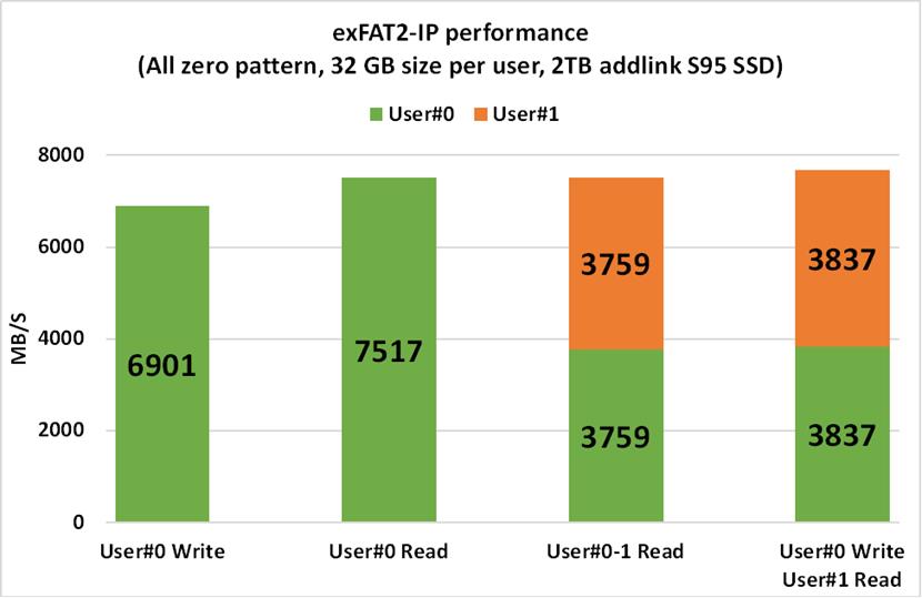
Figure 4‑1 Test Performance of exFAT2-IP demo using Addlink S95 SSD
Utilizing PCIe Gen4 on the VCK190 board, the total performance of a single user, User#0 Write is approximately 6900 Mbyte/sec, while User#0 Read achieves about 7500 Mbyte/sec. For two users, the total performance of User#0-#1 Read is equivalent to the total performance of User#0 Read alone. The performance of each user during the User User#0-#1 Read (3759 MB/s) is approximately half of the performance achieved during User#0 Read (7517 MB/s). Furthermore, the mixed Write-Read file command (User#0 Write, User#1 Read) demonstrates good load balancing under both test conditions. However, when the test conditions change, such as using larger transfer size and random test pattern, the performance of most SSDs tends to decrease.
5 Revision History
|
Revision |
Date |
Description |
|
1.00 |
7-May-24 |
Initial release |
Copyright: 2024 Design Gateway Co,Ltd.