exFAT IP for NVMe reference design manual
Rev1.2 3-Jul-23
3.1 Test firmware (exfatnvmetest.c)
3.1.2 Write file/Read file command
3.2 Function list in Test firmware
1 Introduction
In the hardware system, data stream can be stored to the disk by using raw data or file system. Using raw data, the data is allocated in the disk through physical address. When many data types are stored in one disk, user needs to assign the different address for each data group. Without standard, each system defines the different data structure to arrange data groups independently. It is the problem for the Host to read data from the system which is recorded without standard.
As a result, file system is created to manage data in the disk by setting up the table to be an index of data. The data is separated into many groups. Each group is called a �file�. For system flexibility, one file has some information to represent itself such as file name, file type, file size, and physical address of file data. File information helps user to know file structure and free space in the disk.
exFAT is standard file system which is common support in many platforms. Comparing to FAT32 file system, exFAT file system improves many features. First, exFAT supports more than 4 GB file size and supports more than 2 TB disk capacity. Next, Name hash of file name is implemented to improve search function. Otherwise, checksum is applied in system data area to increase data reliability.
Generally, file system is implemented as standard library running on CPU. To write/read file by using CPU software, it has overhead time to access file header to read file allocation before writing or reading file data. So, write/read performance when running file system by using CPU software is reduced, comparing to using raw data format which does not have the header.
exFAT IP is the hardware which designs file system data structure following exFAT standard. exFAT IP reduces the overhead time to access file header. As a result, write/read performance when using exFAT IP is almost same as raw data format which is run by DG NVMe IP. From the reference design, the performance of Write file command is about 2144 MB/s while the performance of Read file command is about 3251 MB/s.
The hardware design of exFAT IP for NVMe demo is different from the hardware design of NVMe IP design (raw data), as shown in Figure 1‑1.
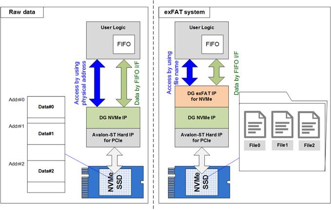
Figure 1‑1 Hardware system for raw data and file system
Comparing to raw data system in the left side of Figure 1‑1, exFAT system includes exFAT IP for NVMe to connect between User Logic and NVMe IP. The parameter of user interface changes from physical parameters (address and length) to be file parameters (file name and the number of files). However, the data interface of raw data and exFAT system are similar by using general FIFO interface. More details of exFAT IP for NVMe reference design are described in the next topic.
2 Hardware overview
The reference design of exFAT IP for NVMe is modified from NVMe IP reference design. exFAT IP is included and the control interface is updated from physical parameters to be file parameters instead. The updated part is displayed as the blue color in Figure 2‑1.
More details of NVMe IP reference design are described in following document.
https://dgway.com/products/IP/NVMe-IP/Altera/dg_satahostip_refdesign_intel_en.pdf
https://dgway.com/products/IP/NVMe-IP/Altera/dg_satahostip_instruction_intel_en.pdf
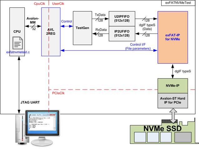
Figure 2‑1 exFAT IP for NVMe demo system
File parameters for control interface of exFAT IP are received from TestGen module. The registers inside Avl2Reg are updated following the control signals of the test system. CPU firmware is updated to receive file parameters from the user and then converts to be the control signals of the hardware through Avalon-MM bus. The example parameters from user are file name, file size, the number of files, created date, and created time.
Four commands are supported by exFAT IP, i.e. Format, Write file, Read file, and Shutdown. The transfer performance is displayed on JTAG UART as a test result after finishing Write file or Read file command. Otherwise, the user can plug-in the NVMe SSD to the other hosts which support exFAT system such as PC to read and verify test data file in the NVMe SSD.
Three clock domains are applied in the system, i.e. CpuClk, UserClk, and PCIeClk. CpuClk is the clock domain of CPU and its peripherals. This clock must be stable clock which is independent from the other hardware interface. PCIeClk is the clock output from PCIe hard IP to synchronous with data stream of 128 bit Avalon stream bus. When the PCIe hard IP is set to 4 lane PCIe Gen3, PCIeClk frequency is equal to 250 MHz. Otherwise, PCIeClk frequency is equal to 125 MHz for PCIe Gen2. UserClk is the example user clock domain which is independent from the other clock domains. So, UserClk is the main clock domain for running the user interface of exFAT IP, NVMe IP, FIFO, and TestGen. According to NVMe IP datasheet, clock frequency of UserClk must be more than or equal to PCIeClk. In this reference design, UserClk is equal to 275 MHz for PCIe Gen3 or 200 MHz for PCIe Gen2.
More details of the hardware in exFAT IP for NVMe demo design are described as follows.
2.1 TestGen
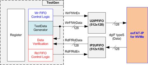
Figure 2‑2 TestGen interface
TestGen module is the test logic to send test data to exFAT IP through U2IPFIFO when operating Write file command. Also, the test data is fed to be the expected value to verify the received data from exFAT IP through IP2UFIFO when operating Read file command. Control logic asserts Write enable and Read enable to �1� when the FIFOs are ready. Data bandwidth of TestGen is matched to exFAT IP by running at the same clock and using same data bus size, so exFAT IP can transfer data with U2IPFIFO and IP2UFIFO without waiting FIFO ready. As a result, the test logic shows the best performance to write and read data with the SATA device through exFAT IP.
Register file in the TestGen receives test parameters from user, i.e. file size, file name, the number of files, the command, verification enable, and test pattern selector. The internal logic includes the counter to control total transfer size of test data. The details of hardware logic of TestGen are shown in Figure 2‑3.
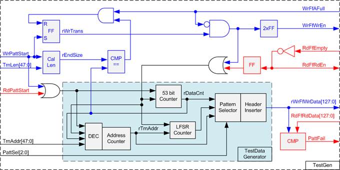
Figure 2‑3 TestGen hardware
As shown in the right side of Figure 2‑3, flow control signals of FIFO are WrFfAFull and RdFfEmpty. When FIFO is almost full during write operation (WrFfAFull=�1�), WrFfWrEn is de-asserted to �0� to pause data sending to FIFO. For read operation, when FIFO has data (RdFfEmpty=�0�), RdFfRdEn is asserted to �1� to read data from FIFO to compare with the expected data.
The logic in the left side of Figure 2‑3 is designed to count transfer size. When total data count is equal to the end size (calculated by UserFLen x File size decoded from DiskFSize), write enable or read enable of FIFO is de-asserted to �0�. So, the total data count to write FIFO or read FIFO is controlled by user.
The lower side of Figure 2‑3 shows the details to generate test data for writing to FIFO or verifying with data from FIFO. There are five patterns to generate, i.e. all zero, all one, 32 bit increment data, 32 bit decrement data, and LFSR counter. All zero and all one are fixed value to select test data through Pattern Selector. 32 bit increment data is designed by using 53 bit counter while the decrement data can be designed by connecting NOT logic to increment data. The LFSR pattern is designed by using LFSR counter. The equation of LFSR is x^31 + x^21 + x + 1. Data bus size of TestGen is 128 bit, so four 32-bit LFSR data must be generated within one clock. The logic to design LFSR must use look-ahead style to generate four LFSR data in the same clock.
To create unique test data for every 512 byte data, test pattern is designed as shown in Figure 2‑4.
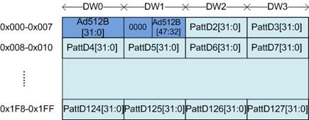
Figure 2‑4 Test pattern format in each 512 byte data
512 byte data consists of two parts, i.e. 64 bit header in Dword#0 and Dword#1 and test data in Dword#2 � Dword#127. 64 bit header is created by using the address in 512 byte unit. So, Address counter inside TestData Generator is designed to generate the current address for 64 bit header data. The initial value of the address counter is calculated by UserFName x File size decoded from DiskFSize. After that, the address counter is increment when finishing transferring 512 byte data.
Test data uses Ad512B (the address in 512 byte unit) to be the start value of test pattern in each block. Test data is fed to be the data input to the FIFO or the expected data for comparing with the data output from FIFO. Fail flag is asserted to �1� when data verification is failed. The example of timing diagram to write data to FIFO is shown as follows.
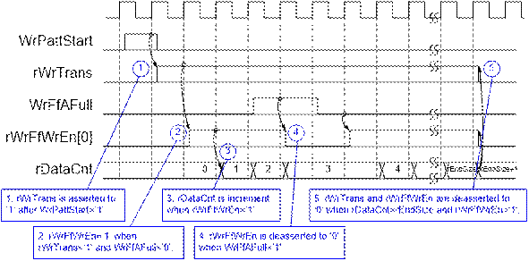
Figure 2‑5 Timing diagram of Write operation in TestGen
1) WrPattStart is asserted to �1� for one clock cycle when user sets the register to start Write file operation. In the next clock, rWrTrans is asserted to �1� to enable the control logic for generating write enable to FIFO.
2) Write enable to FIFO (rWrFfWrEn) is asserted to �1� when two conditions are met. First, rWrTrans must be asserted to �1� during running the write operation. Second, the FIFO must not be full by monitoring WrFfAFull=�0�.
3) The write enable is fed back to be counter enable to count total data in the write operation.
4) If FIFO is almost full (WrFfAFull=�1�), the write process will be paused by de-asserting rWrFfWrEn to �0�.
5) When total data count is equal to the set value, rWrTrans is de-asserted to �0�. At the same time, rWrFfWrEn is also de-asserted to �0� to stop data generating.
For read timing diagram, read enable of FIFO is controlled by empty flag of FIFO. Comparing to write enable, the read enable signal is not stopped by total count and not started by start flag. When the read enable is asserted to �1�, the data counter and the address counter are also increment for counting total data and generating the header of expect value.
2.2 exFAT
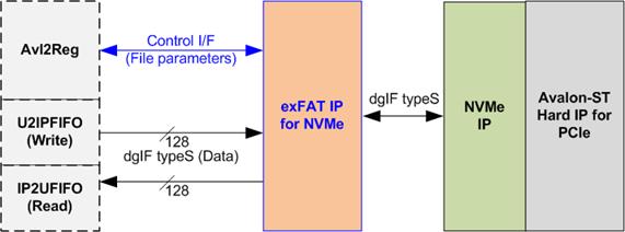
Figure 2‑6 exFAT hardware
As shown in Figure 2‑6, the user interface of exFAT IP is split into two groups, i.e. the control interface and the data interface. The control interface is connected to Avl2Reg to receive file parameters from user through JTAG UART. The data interface is 128 bit data bus and connects with U2IPFIFO and IP2UFIFO. Another side of exFAT IP is connected to NVMe IP.
2.2.1 exFAT IP for NVMe
exFAT IP implements the logic to handle data in NVMe device following exFAT file system. exFAT IP must be integrated with NVMe IP. Data bus size is 128 bit. More details of exFAT IP for NVMe are described in datasheet.
https://dgway.com/products/IP/NVMe-IP/dg_exfatip_nvme_data_sheet_intel_en.pdf
2.2.2 NVMe IP
NVMe IP implements NVMe protocol of the host side to access one NVMe device directly without PCIe switch connection. User interface is simply designed by using dgIF typeS format. NVMe IP is designed to connect with Avalon-ST Hard IP for PCIe (Hard IP in Intel FPGA device). More details of NVMe IP are described in datasheet.
https://dgway.com/products/IP/NVMe-IP/dg_nvmeip_datasheet_intel_en.pdf
2.2.3 Avalon-ST PCIe Hard IP
This block is hard IP in Intel FPGA device which implements Physical, Data Link, and Transaction Layers of PCIe specification. More details are described in Intel FPGA document.
ArriaV Avalon-ST Interface for PCIe Solutions User Guide
https://www.altera.com/en_US/pdfs/literature/ug/ug_a5_pcie_avst.pdf
Stratix V Avalon-ST Interface for PCIe Solutions User Guide
https://www.altera.com/en_US/pdfs/literature/ug/ug_s5_pcie_avst.pdf
Intel Arria10 Avalon-ST Interface for PCIe Solutions User Guide
https://www.altera.com/en_US/pdfs/literature/ug/ug_a10_pcie_avst.pdf
2.3 CPU and Peripherals
32 bit Avalon-MM is applied to be the bus interface for CPU accessing the peripherals such as Timer and JTAG UART. To control and monitor the test logic of exFAT IP, the test logic is connected to CPU as a peripheral on 32 bit Avalon-MM bus. CPU assigns the different base address and the address range for each peripheral.
In the reference design, the CPU system is built with one additional peripheral to access the test logic. The base address and the range for accessing the test logic are defined in the CPU system. So, the hardware logic must be designed to support Avalon-MM bus standard for writing and reading the register. Avl2Reg module is designed to connect the CPU system as shown in Figure 2‑7.
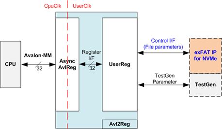
Figure 2‑7 CPU and peripherals hardware
Avl2Reg consists of AsyncAvlReg and UserReg. AsyncAvlReg is designed to convert the Avalon-MM signals to be the simple register interface which has 32 bit data bus size (same as Avalon-MM data bus size). Otherwise, AsyncAvlReg includes asynchronous logic to support clock crossing between CpuClk domain and UserClk domain.
UserReg includes the register file of the parameters and the status signals to control the other modules, i.e. exFAT IP and TestGen. More details of AsyncAvlReg and UserReg are described as follows.
2.3.1 AsyncAvlReg
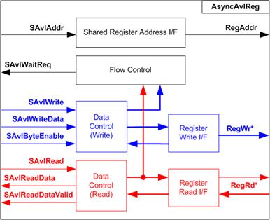
Figure 2‑8 AsyncAvlReg Interface
The signal on Avalon-MM bus interface can be split into three groups, i.e. Write channel (blue color), Read channel (red color) and Shared control channel (black color). More details of Avalon-MM interface specification is described in following document.
https://www.intel.com/content/dam/www/programmable/us/en/pdfs/literature/manual/mnl_avalon_spec.pdf
According to Avalon-MM specification, one command (write or read) can be operated at a time. The logic inside AsyncAvlReg is split into three groups, i.e. Write control logic, Read control logic and Flow control logic. Flow control logic to control SAvlWaitReq is designed to hold the next request from Avalon-MM interface while the current request is operating. Write control I/F and Write data I/F of Avalon-MM bus are latched and transferred as Write register. Otherwise, Read control I/F and Read data I/F of Avalon-MM bus are latched and transferred as Read register. Address I/F of Avalon-MM is latched and transferred to Address register interface as well.
The simple register interface is designed to compatible to general RAM interface for write transaction. The read transaction of the register interface is little modified from RAM interface by adding RdReq signal. The address of register interface is shared for write and read transaction. So, user cannot write and read the register at the same time. The timing diagram of the register interface is shown in Figure 2‑9.
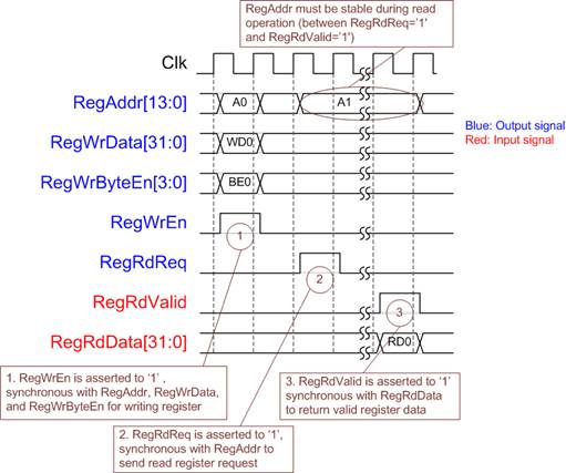
Figure 2‑9 Register interface timing diagram
1) To write register, the timing diagram is same as general RAM interface. RegWrEn is asserted to �1� with the valid signal of RegAddr (Register address in 32 bit unit), RegWrData (write data of the register), and RegWrByteEn (the write byte enable). Byte enable has four bit to be the byte data valid, i.e. bit[0] for RegWrData[7:0], bit[1] for RegWrData[15:8], and so on.
2) To read register, AsyncAvlReg asserts RegRdReq to �1� with the valid value of RegAddr. 32 bit data must be returned after receiving the read request. The slave must monitor RegRdReq signal to start the read transaction.
3) The read data is returned on RegRdData bus by the slave with asserting RegRdValid to �1�. After that, AsyncAvlReg forwards the read value to SAvlRead interface.
2.3.2 UserReg
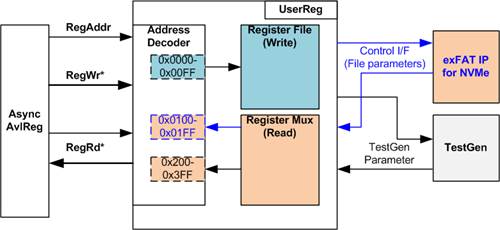
Figure 2‑10 UserReg Interface
The address range to map to UserReg is split into three areas, as shown in Figure 2‑10.
1) 0x0000 � 0x00FF: mapped to set the test parameters of exFAT IP and TestGen. This area is write access only.
2) 0x0100 � 0x01FF: mapped to read the status of exFAT IP. This area is read access only.
3) 0x0200 � 0x02FF: mapped to read the status of TestGen. This area is read access only.
Address decoder decodes the upper bit of RegAddr for selecting the active hardware. The register file inside UserReg is 32 bit size, so write byte enable (RegWrByteEn) is not used. To set the parameters in the hardware, the CPU must use 32 bit pointer to force 32 bit valid value of the write data.
To read register, two step multiplexers are designed. Register Mux is the data multiplexer to select the read data within each address area. The lower bit of RegAddr is applied in the Register Mux. Next, the address decoder uses the upper bit to select the read data from each area for returning to CPU. Totally, the latency of read data is equal to two clock cycles, so RegRdValid is created by RegRdValid with asserting two D Flip-flips.
More details of the address mapping within UserReg module is shown in Table 2‑1.
Table 2‑1 Register Map
|
Address |
Register Name |
Description |
|
Rd/Wr |
(Label in the �exfatnvmetest.c�) |
|
|
0x0000 � 0x00FF: Control signals of exFAT IP and TestGen (Write access only) |
||
|
BA+0x000 |
User File Name Reg |
[26:0]: Input to be UserFName of exFAT IP for NVMe |
|
(USRFNAME _REG) |
||
|
BA+0x004 |
User File Length Reg |
[26:0]: Input to be UserFLen of exFAT IP for NVMe |
|
(USRFLEN _REG) |
||
|
BA+0x008 |
File Size Reg |
[2:0]: Input to be FSize of exFAT IP for NVMe. Comparing to DFSIZE_REG, this input is used to set File size to exFAT IP for NVMe during running Format command. |
|
(USRFSIZE _REG) |
||
|
BA+0x00C |
Created Date and Time Reg |
[4:0]: Input to be FTimeS of exFAT IP for NVMe [10:5]: Input to be FTimeM of exFAT IP for NVMe [15:11]: Input to be FTimeH of exFAT IP for NVMe [20:16]: Input to be FDateD of exFAT IP for NVMe [24:21]: Input to be FDateM of exFAT IP for NVMe [31:25]: Input to be FDateY of exFAT IP for NVMe |
|
(DATETIME_REG) |
||
|
BA+0x010 |
User Command Reg |
[1:0]: Input to be UserCmd of exFAT IP for NVMe When this register is written, the design asserts UserReq=�1� (command request) to exFAT IP for NVMe to start new command operation. |
|
(USRCMD _REG) |
||
|
BA+0x014 |
Pattern Select Reg |
[2:0]: Test pattern select �000�-Increment, �001�-Decrement, �010�-All 0, �011�-All 1, �100�-LFSR |
|
(PATTSEL_REG) |
||
|
0x0100 � 0x01FF: Status signals of exFAT IP (Read access only) |
||
|
BA+0x100 |
User Status Reg |
[0]: Mapped to UserBusy of exFAT IP for NVMe [1]: Mapped to UserError of exFAT IP for NVMe [2]: Data verification fail (�0�: Normal, �1�: Error) |
|
(USRSTS_REG) |
||
|
BA+0x104 |
Total file capacity Reg |
[26:0]: Mapped to TotalFCap[26:0] of exFAT IP for NVMe |
|
(TOTALFCAP_REG) |
||
|
BA+0x108 |
User Error Type Reg |
[31:0]: Mapped to UserErrorType[31:0] of exFAT IP for NVMe |
|
(USRERRTYPE_REG) |
||
|
BA+0x10C |
exFAT IP Test pin (Low) Reg |
[31:0]: Mapped to TestPin[31:0] of exFAT IP for NVMe |
|
(FATTESTPINL_REG) |
||
|
BA+0x110 |
exFAT IP Test pin (High) Reg |
[31:0]: Mapped to TestPin[63:32] of exFAT IP for NVMe |
|
(FATTESTPINH_REG) |
||
|
BA+0x114 |
Directory capacity Reg |
[19:0]: Mapped to DirCap[19:0] of exFAT IP for NVMe
|
|
(DIRCAP_REG) |
||
|
BA+0x118 |
File Size in the disk Reg |
[2:0]: Mapped to DiskFsize of exFAT IP for NVMe. Comparing to USRFSIZE_REG, this is the current file size which exFAT IP reads from the device. |
|
(DFSIZE_REG) |
||
|
BA+0x11C |
Total file in the disk Reg |
[26:0]: Mapped to DiskFnum of exFAT IP for NVMe |
|
(DFNUM_REG) |
||
|
BA+0x120 |
Disk Capacity (Low) Reg |
[31:0]: Mapped to LBASize(bit[31:0]) of NVMe IP to check total capacity of the disk. |
|
(DFSIZEL_REG) |
||
|
BA+0x124 |
Disk Capacity (High) reg |
[15:0]: Mapped to LBASize(bit[47:32]) of NVMe IP to check total capacity of the disk. |
|
(DFSIZEH_REG) |
||
|
BA+0x128 |
Completion Status Reg |
[15:0]: Status from Admin completion (AdmCompStatus[15:0] of NVMe IP) [31:16]: Status from I/O completion (IOCompStatus[15:0] of NVMe IP) |
|
(COMPSTS_REG) |
||
|
BA+0x12C |
NVMe CAP Reg |
[31:0]: NVMeCAPReg[31:0] output from NVMe IP |
|
(NVMCAP_REG) |
||
|
BA+0x130 |
NVMe Test pin (Low) Reg |
[31:0]: Mapped to TestPin[31:0] NVMe IP |
|
(NVMTESTPIN_REG ) |
||
|
Address |
Register Name |
Description |
|
Rd/Wr |
(Label in the �exfatnvmetest.c�) |
|
|
0x0200 � 0x02FF: Status signals of TestGen (Read access only) |
||
|
BA+0x200 |
Expected value Word0 Reg |
[31:0]: Bit[31:0] of the expected data at the 1st failure data |
|
(EXPPATW0_REG) |
||
|
BA+0x204 |
Expected value Word1 Reg |
[31:0]: Bit[63:32] of the expected data at the 1st failure data |
|
(EXPPATW1_REG) |
||
|
BA+0x208 |
Expected value Word2 Reg |
[31:0]: Bit[95:64] of the expected data at the 1st failure |
|
(EXPPATW2_REG) |
||
|
BA+0x20C |
Expected value Word3 Reg |
[31:0]: Bit[127:96] of the expected data at the 1st failure |
|
(EXPPATW3_REG) |
||
|
BA+0x210 |
Read value Word0 Reg |
[31:0]: Bit[31:0] of the read data at the 1st failure data |
|
(RDPATW0_REG) |
||
|
BA+0x214 |
Read value Word1 Reg |
[31:0]: Bit[63:32] of the read data at the 1st failure data |
|
(RDPATW1_REG) |
||
|
BA+0x218 |
Read value Word2 Reg |
[31:0]: Bit[95:64] of the read data at the 1st failure data |
|
(RDPATW2_REG) |
||
|
BA+0x21C |
Read value Word3 Reg |
[31:0]: Bit[127:96] of the read data at the 1st failure data |
|
(RDPATW3_REG) |
||
|
BA+0x220 |
Failure Byte Address (Low) Reg |
[31:0]: Bit[31:0] of the byte address in the file at the 1st failure data |
|
(FAILADDRL_REG) |
||
|
BA+0x224 |
Failure Byte Address (High) Reg |
[6:0]: Bit[38:32] of the byte address in the file at the 1st failure data |
|
(FAILADDRH_REG) |
||
|
BA+0x228 |
Failure File Name Reg |
[26:0]: Filename of the 1st failure data |
|
(FAILFNAME_REG) |
||
|
BA+0x22C |
Current test byte (Low) Reg |
[31:0]: Bit[31:0] of the current test data size in TestGen module |
|
(CURTESTSIZEL_REG) |
||
|
BA+0x230 |
Current test byte (High) Reg |
[24:0]: Bit[56:32] of the current test data size in TestGen module |
|
(CURTESTSIZEH_REG) |
||
|
Other interfaces |
||
|
BA+0x800 |
IP Version Reg |
[31:0]: IP version number, mapped to IPVersion [31:0] of exFAT IP for NVMe |
|
(IPVERSION_REG) |
||
3 CPU Firmware
3.1 Test firmware (exfatnvmetest.c)
After system boot-up, CPU starts the initialization sequence as follows.
1) CPU initializes its peripherals such as UART and Timer.
2) CPU waits until exFAT IP completes initialization process (USRSTS_REG[0]=�0�).
3) CPU reads the disk information.
4) Receive the input from user to run format the disk or not.
In case of start up without format,
a) CPU loads the default parameter to set to exFAT IP.
b) The current system information is displayed on the console. Three parameters which are outputs of exFAT IP are read by CPU to show on the console, i.e. current file size (DFSIZE_REG), total file in the disk (DFNUM_REG), and maximum file to store in the disk (TOTALFCAP_REG).
In case of start up with format, the next step is same as running Format command menu.
5) After all parameters are set completely, main menu is displayed on the console. There are four commands for the test, i.e. Format command (USRCMD_REG=�00�), Write file command (USRCMD_REG=�10�), Read file command (USRCMD_REG=�11�), and Shutdown command (USRCMD_REG=�01�).
More details of the operation sequence for each command are described as follows.
3.1.1 Format
The sequence of the firmware when user selects Format menu is below.
1) Ask user to set created date and created time of directory or use default value. Then, set the value to DATETIME_REG.
2) Read disk capacity from DCAPH/L_REG and calculate supported file size to display on the console.
3) Ask user to set file size and then set the value to USRFSIZE_REG.
4) Set USRCMD_REG=�00� to run Format command. After that, exFAT IP changes to busy status (USRSTS_REG[0] changes from �0� to �1�).
5) CPU waits until the operation is completed or some errors are found by monitoring USRSTS_REG[1:0].
Bit[0] is de-asserted to �0� when command is completed.
Bit[1] is asserted to �1� when some errors are detected. In case of error condition, error message is displayed on the console.
6) If the command is completed, the disk information will be displayed, i.e. maximum file in the disk (TOTALFCAP_REG), maximum file per directory (DIRCAP_REG), current file size (DFSIZE_REG), and total file in the disk (DFNUM_REG).
3.1.2 Write file/Read file command
The sequence of the firmware when user selects Write file/Read file command is below.
1) Skip to the next step for Read file command. For Write file command, ask user to set created date and created time of directory or use default value. Then, set the value to DATETIME_REG.
2) In case of Write command,
a) Ask user to use default Start file No. which continues from previous Write file command or change to other value.
b) If the input is valid, the new value will be set to USRFNAME_REG.
In case of Read command,
a) Receive Start file No. from user.
b) If the input is valid, the new value will be set to USRFNAME_REG.
3) Receive total files and test pattern through Serial console. If some inputs are invalid, the operation will be cancelled.
4) Set the inputs to USRFLEN_REG and PATTSEL_REG.
5) Send Write file or Read file command by setting USRCMD_REG (�10� for Write file command or �11� for Read file command).
6) CPU waits until the operation is completed or some errors (except verification error) are found by monitoring USRSTS_REG[2:0].
Bit[0] is de-asserted to �0� when command is completed.
Bit[1] is asserted when error is detected. After that, error message is displayed on the console to show the error details. Finally, the process will be cancelled.
Bit[2] is asserted when data verification is failed. Then, the verification error message is displayed. CPU is still running until the operation is done or user inputs any key to cancel operation.
During running command, current transfer size reading from CURTESTSIZE_REG is displayed every second.
7) After busy flag (USRSTS_REG[0]) is de-asserted to �0�, CPU displays the test result on the console, i.e. total time usage, total transfer size, and transfer speed.
3.1.3 Shutdown Command
The sequence of the firmware when user selects Shutdown command is below.
1) Set USRCMD_REG=�01� to run Shutdown command. After that, exFAT IP changes to busy status (USRSTS_REG[0] changes from �0� to �1�).
2) CPU waits until the operation is completed or some errors are found by monitoring USRSTS_REG[1:0].
Bit[0] is de-asserted to �0� when command is completed.
Bit[1] is asserted to �1� when some errors are detected. In case of error condition, error message is displayed on the console.
3) If the command is completed, the device will change to inactive status. CPU does not receive any new command. User should power off system after completing this command.
3.2 Function list in Test firmware
|
void change_ftime(void) |
|
|
Parameters |
None |
|
Return value |
None |
|
Description |
Print current create time and date by calling show_ftime function. After that, ask user to change the value. If input is valid, the created time and date will be updated to DATETIME_REG and global parameter (DateTime). |
|
int format_fat(void) |
|
|
Parameters |
None |
|
Return value |
0: User cancels command or command is finished. -1: Receive invalid input or error is found. |
|
Description |
Run Format command, following in topic �Դ��Ҵ! ��辺���觡����ҧ�ԧ |
|
unsigned long long get_cursize(void) |
|
|
Parameters |
None |
|
Return value |
Read value of CURTESTSIZEH/L_REG |
|
Description |
Read CURTESTSIZEH/L_REG and return read value as function result. |
|
int get_param(userin_struct* userin, unsigned int user_cmd) |
|
|
Parameters |
userin: Three inputs from user, i.e. start file number, number of file, and test pattern user_cmd: 2-Write file command and 3-Read file command |
|
Return value |
0: Valid input, -1: Invalid input |
|
Description |
Read user_cmd and then calculates input parameter range to display on the console. After receiving user input, the value is verified. If input is invalid, the function will be returned by -1. Otherwise, all inputs are updated to userin parameter. |
|
int wrrd_file(unsigned int user_cmd) |
|
|
Parameters |
Command from user (2: Write file command, 3: Read file command) |
|
Return value |
0: Operation is successful. -1: Receive invalid input or error is found. |
|
Description |
Run Write file or Read file command, following in topic �Դ��Ҵ! ��辺���觡����ҧ�ԧ |
|
void show_dir(userin_struct* userin, unsigned int user_cmd) |
|
|
Parameters |
User input, i.e. file name and number of file and User command |
|
Return value |
None |
|
Description |
Print file name and directory of the 1st file and the last file which are written/read in the current command. Print file name and directory of the last file in the device. |
|
void show_diskinfo(void) |
|
|
Parameters |
None |
|
Return value |
None |
|
Description |
Print the current disk information from global parameters, i.e. file size (DFnumB), maximum file in the disk (TotalFCap), maximum file per directory (DirCap), and total file in the disk (DFnum). |
|
void show_error(void) |
|
|
Parameters |
None |
|
Return value |
None |
|
Description |
Read USRERRTYPE_REG and decode the value. Print error type when the flag is found. The example of error type is timeout error, NVMe IP error, unsupported disk capacity, or unsupported LBA size. |
|
void show_ftime(void) |
|
|
Parameters |
None |
|
Return value |
None |
|
Description |
Print current created date and time from global parameter (DateTime) |
|
void show_size(unsigned long long size_input) |
|
|
Parameters |
Size in byte unit |
|
Return value |
None |
|
Description |
Print input value in MB, GB, or TB unit |
|
void show_result(void) |
|
|
Parameters |
None |
|
Return value |
None |
|
Description |
Print total size by calling get_cursize and show_size function. After that, calculate total time usage from global parameters (timer_val and timer_upper_val) and display in usec, msec, or sec unit. Finally, transfer performance is calculated and displayed on MB/s unit. |
|
void show_vererr(void) |
|
|
Parameters |
None |
|
Return value |
None |
|
Description |
Print information from hardware register to show verification error details, i.e. the 1st error file name (FAILFNAME_REG), the 1st error address (FAILADDRL/H_REG), expected value (EXPPATW0-3_REG), and error read value (RDPATW0-3_REG). |
|
int shutdown_dev (void) |
|
|
Parameters |
None |
|
Return value |
0: Shutdown command is finished. -1: User cancels command or error is found. |
|
Description |
Run Shutdown command, following in topic �Դ��Ҵ! ��辺���觡����ҧ�ԧ |
|
void update_dfsize(void) |
|
|
Parameters |
None |
|
Return value |
None |
|
Description |
Read total file (TOTALFCAP_REG) and current file size in the disk (DFSIZE_REG) from hardware. File size is decoded and converted to be byte unit. Finally, total file and file size are updated to global parameters (TotalFCap and DFsizeB). |
|
void update_dfnum(void) |
|
|
Parameters |
None |
|
Return value |
None |
|
Description |
Read total file in the disk from DFNUM_REG, and then update read value to global parameter (DFnum). |
4 Example Test Result
The example test result when running demo system by using 512 GB Samsung 960 Pro is shown in Figure 4‑1.
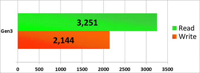
Figure 4‑1 Test Performance of exFAT IP demo for NVMe by using Samsung 960 Pro SSD
By using PCIe Gen3 on Arria10 GX development kit, write performance is about 2144 Mbyte/sec and read performance is about 3251 Mbyte/sec.
5 Revision History
|
Revision |
Date |
Description |
|
1.0 |
22-Jan-19 |
Initial release |
|
1.1 |
22-Mar-19 |
- Add DiskFsize, DiskFnum signal - Add function list |
|
1.2 |
14-May-19 |
Update Dircap size and the design details |
Copyright: 2019 Design Gateway Co,Ltd.