FAT32 IP Core for NVMe Data Sheet

Core Facts |
|
|
Provided with Core |
|
|
Documentation |
Reference Design Manual Demo Instruction Manual |
|
Design File Formats |
Encrypted hdl File |
|
Instantiation Templates |
VHDL |
|
Reference Designs & Application Notes |
QuartusII Project, See Reference Design Manual |
|
Additional Items |
Demo on Arria10 SoC/Arria10 GX Development Kit |
|
Support |
|
|
Support Provided by Design Gateway Co., Ltd. |
|
Design Gateway Co.,Ltd
54 BB Building 14th Fl., Room No.1402 Sukhumvit 21 Rd. (Asoke), Klongtoey-Nua, Wattana, Bangkok 10110
Phone: 66(0)2-261-2277
Fax: 66(0)2-261-2290
E-mail: ip-sales@design-gateway.com
URL: www.design-gateway.com
Features
· Simple user interface
· Operating with DG NVMe IP Core
· Implement FAT32 file system management without CPU usage
· Maximum write speed up to 2100 MB/s and read speed up to 3200 MB/s
· Support SSD capacity: 64 MB – 2 TB
· Support three commands, i.e. Format, Write file, and Read file
· Support seven file sizes, i.e. 32MB, 64MB, 128MB, 256MB, 512MB, 1024MB, 2048MB
· Reference design with AB16-PCIeXOVR adapter board available on Arria10 GX development board and without adapter on Arria10 SoC development board.
·
Table 1: Example Implementation Statistics
|
Family |
Example Device |
Fmax (MHz) |
Logic utilization (ALMs) |
Registers1 |
Pin |
Block Memory bit |
Design Tools |
|
Arria10 SX |
10AS066N3F40E2SG |
280 |
835 |
1277 |
- |
41,984 |
QuartusII 16.0 |
Notes:
1) Actual logic resource dependent on percentage of unrelated logic
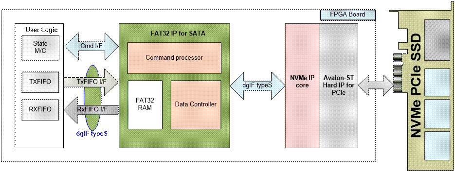
Figure 1: FAT32 IP for NVMe Block Diagram
Applications
FAT32 IP Core for NVMe operating with DG NVMe IP core and Avalon-ST PCIe Hard IP from Intel is an ideal to access NVMe PCIe SSD by using FAT32 File system management without CPU and external memory. It can transfer data as a file in FAT32 format as fast as raw data transfer. The data transfer speed can be raised up to the maximum limit of NVMe PCIe SSD by using FAT32 IP Core combined with DG NVMe IP core and Avalon-ST PCIe Hard IP. The IP is recommended for application which requires ultra high-speed data recording system and the data in SSD is processed by the system which can access FAT32 format.
General Description
FAT32 IP Core for NVMe is designed to transfer data as FAT32 file system to NVMe PCIe SSD by interfacing between user logic and NVMe IP core. User can transfer data to NVMe PCIe SSD as a file in FAT32 file system standard instead of raw data. In general system, data format in NVMe PCIe SSD when using NVMe IP Core is raw data. When user connects the SSD to other systems, it needs to use special software to access the SSD as raw data. FAT32 file system is well known and generally used in many systems, so user can read data from the SSD without special software.
FAT32 IP Core for NVMe supports three commands, i.e. Format, Write file, and Read file. FAT32 IP Core can work with varieties of SSD capacity from 64 MB – 2 TB with only one partition, stored data as a file with adjustable file size from 32MB - 2GB per file. Once the SSD is writtten, file size cannot be changed until it is formatted.
User interface of FAT32 IP Core for NVMe has two groups, i.e. control and data. Control interface is almost similar to dgIF typeS, but physical address and length are replaced by file number and numbers of file. Data interface of FAT32 IP Core is dgIF typeS interface.
Clock domain of FAT32 IP Core for NVMe is same as NVMe IP’s user clock.
Functional Description
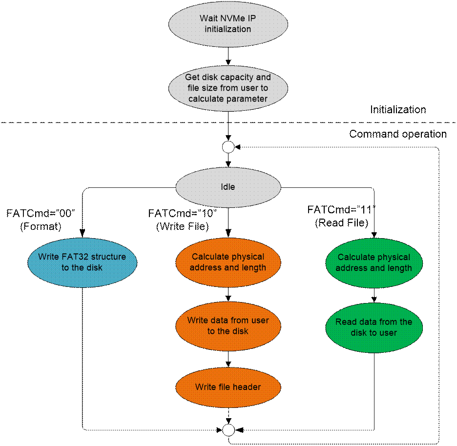
Figure 2: FAT32 IP for NVMe Operation
The sequence of FAT32 IP Core for NVMe operation is as follows:
1) IP waits NVMe IP to complete device initialization.
2) IP sends Identify command to NVMe IP to get SSD capacity. File size input from user and SSD capacity are used to calculate FAT32 parameters. After that, IP is ready to wait command from user. Three commands can be selected, i.e. Format, Write file, and Read file.
3) a. Format command is required to set up file system in the SSD and clean up the SSD. If file size parameter is changed, the maximum numbers of file in the SSD will be changed. So, Format commmand is required when file size is changed.
In Format command, the IP writes FAT32 file structure such as Master Boot Record and root directory to the SSD.
b. When user select Write command, the 1st file name and numbers of file (inputs from user) are received to calculate the start physical address and total length to write the SSD by user data. Data from user is transferred to the SSD continuously until end of transfer. After that, the IP writes file header to complete file operation.
Note:
1. File header is filled to the SSD in the final step. If system is powered down before the header is filled, the new file will be lost and will not found in the SSD.
2. There is no protection if the input from user is out-of-range.
c. Similar to Write command, the 1st process of Read command is to calculate start physical address and total length to read the SSD from user input. Data from SSD is transferred to user until end of transfer.
FAT32 IP for NVMe
As shown in Figure 1, there are three submodules inside the IP, i.e. Command processor, Data Controller, and FAT32 RAM. Command processor receives command from user logic, converts the inputs to internal parameters and sends the command to NVMe IP. Data controller is designed to transfer data between FIFOs in user logic to NVMe IP. Data sending to NVMe IP has two types, i.e. user data and file system data. Most of File system data are stored in FAT32 RAM. More details of each submodules are described as follows.
l Command processor
This module includes state machine to control the IP operation to follow the sequence in Figure 2. There are many calculation units in this block to calculate FAT32 parameters and the physical address of system area in FAT32 file system from user inputs and SSD capacity. The command interface of user logic and NVMe IP are connected to this block. Also, it calculates the parameters and generates control signals to Data controller.
l FAT32 RAM
This RAM is designed by simple dual port RAM.The size is 256x128-bit. FAT32 file system data is stored in this RAM.
l FAT32 Data Controller
This module is desigend to control data flow between user logic and NVMe IP. To create file in the SSD, three data sources are transferred to NVMe IP, i.e. user data from TxFIFO in user logic, FAT32 file system data from FAT32 RAM, and FAT32 parameters from internal registers.
NVMe IP
Details of NVMe IP are described in the datasheet and can be downloaded from our website.
http://www.dgway.com/products/IP/NVMe-IP/dg_nvmeip_datasheet_intel_en.pdf
User Logic
Simple logic which can be designed by using small state machine to send command, file number, and file size. Two FIFOs are used to connect with data interface of FAT32 IP for NVMe. One is used for Write command and another is used for Read command.
Core I/O Signals
Descriptions of all signal I/O are provided in Table 2.
Table 2: Core I/O Signals
|
Signal |
Dir |
Description |
|
System signal |
||
|
RstB |
In |
Synchronous reset signal. Active low. Deassert to ‘1’ when Clk signal is stable. |
|
Clk |
In |
User clock. Must use the same clock as NVMe IP. (125 MHz for PCIe Gen2, 250 MHz for PCIe Gen3). |
|
FSize[2:0] |
In |
File size: “000” : 32MB, “001” : 64MB, “010” : 128MB, “011” : 256MB, “100” : 512MB, “101” : 1024MB, “110” : 2048MB, “111”: Reserved Note: 1) 1 MB is 1024x1024 byte 2) FSize must not be changed when there are files in the SSD. When FSize value is changed, user logic must send Format command to the IP. |
|
FDateY[6:0] |
In |
Year in created date, count from 1980 (For example, FDateY=37 is year 2017). This input is used in write file command. The value must not be changed during write operation. |
|
FDateM[3:0] |
In |
Month in created date. Valid from 1-12 (1=Jan, 2= Feb, …). This input is used in write file command. The value must not be changed during write operation. |
|
FDateD[4:0] |
In |
Day in created date. Valid from 1-31. This input is used in write file command. The value must not be changed during write operation. |
|
FTimeH[4:0] |
In |
Hour in created time. Valid from 0-23. This input is used in write file command. The value must not be changed during write operation. |
|
FTimeM[5:0] |
In |
Minute in created time. Valid from 0-59. This input is used in write file command. The value must not be changed during write operation. |
|
FTImeS[4:0] |
In |
x2 sec in created time. Valid from 0-29 (1=2, 2=4, …). This input is used in write file command. The value must not be changed during write operation. |
|
User Interface (Command) |
||
|
UserCmd[1:0] |
In |
User Command. “00”: Format command, “01” Reserved, “10”: Write file, ”11”: Read file. |
|
UserFName[15:0] |
In |
The 1st file name to write/read file (0= FILE0000.BIN, 1=FILE0001.BIN, …). Valid form 0 to TotalFCap - 1. |
|
UserFLen[15:0] |
In |
Total files transfer in the request. Valid from 1 to (TotalFCap – UserFName). |
|
UserReq |
In |
Request the new command. Can be asserted only when the IP is Idle (UserBusy=’0’). Asserted with valid value on UserCmd, UserFName, and UserFLen signals. |
|
UserBusy |
Out |
IP Busy status. New request will not be allowed if this signal is asserted to ‘1’. |
|
TotalFCap[15:0] |
Out |
Maximum numbers of file which the SSD can store. This value is updated after FAT32-IP completes initialization process. |
|
UserError |
Out |
Direct mapped to NVMeError siganl. Please see more details in NVMe IP datasheet. |
|
UserErrorType[31:0] |
Out |
Direct mapped to NVMeErrorType siganl. Please see more details in NVMe IP datasheet. |
|
TesPin[63:0] |
Out |
Reserved to be IP test point. |
|
Signal |
Dir |
Description |
|
User Interface (Data) |
||
|
UserFifoWrCnt[15:0] |
In |
Write data counter of received FIFO. Used to check full status. If total FIFO size is less than 16-bit, please fill ‘1’ to upper bit. UserFifoWrEn is asserted when UserFifoWrCnt[15:3] is not equal to all 1. |
|
UserFifoWrEn |
Out |
Write data valid of received FIFO. |
|
UserFifoWrData[127:0] |
Out |
Write data bus of received FIFO. Synchronous to UserFifoWrEn. |
|
UserFifoRdCnt[15:0] |
In |
Read data counter of transmit FIFO. Used to check data available size in FIFO. If total FIFO size is less than 16-bit, please fill ‘0’ to upper bit. This signal is unused for this IP. |
|
UserFifoEmpty |
In |
FIFO empty flag of transmit FIFO to check data available status. |
|
UserFifoRdEn |
Out |
Read valid of transmit FIFO. |
|
UserFifoRdData[127:0] |
In |
Read data returned from transmit FIFO. Valid after UserFifoRdEn asserted about one clock period. |
|
NVMe IP User Interface (Connect to dgIF typeS of NVMe IP) (Please see more details from NVMe IP datasheet) |
||
|
NVMeCmd[1:0] |
Out |
Connect to UserCmd of NVMe IP |
|
NVMeAddr[47:0] |
Out |
Connect to UserAddr of NVMe IP |
|
NVMeLen[47:0] |
Out |
Connect to UserLen of NVMe IP |
|
NVMeReq |
Out |
Connect to UserReq of NVMe IP |
|
NVMeBusy |
In |
Connect to UserBusy of NVMe IP |
|
NVMeLBASize[47:0] |
In |
Connect to LBASize of NVMe IP |
|
NVMeError |
In |
Connect to UserError of NVMe IP |
|
NVMeErrorType[31:0] |
In |
Connect to UserErrorType of NVMe IP |
|
NVMeFifoWrCnt[15:0] |
Out |
Connect to UserFifoWrCnt of NVMe IP |
|
NVMeFifoWrEn |
In |
Connect to UserFifoWrEn of NVMe IP |
|
NVMeFifoWrData[127:0] |
In |
Connect to UserFifoWrData of NVMe IP |
|
NVMeFifoRdCnt[15:0] |
Out |
Connect to UserFifoRdCnt of NVMe IP |
|
NVMeFifoEmpty |
Out |
Connect to UserFifoEmpty of NVMe IP |
|
NVMeFifoRdEn |
In |
Connect to UserFifoRdEn of NVMe IP |
|
NVMeFifoRdData[127:0] |
Out |
Connect to UserFifoRdData of NVMe IP |
Timing Diagram
Initialization
After RstB is deasserted, UserBusy flag is set to ‘1’. After the initialization process is completed, UserBusy is deasserted to ‘0’. The IP is ready to receive new command and TotalFCap signal is valid as shown in Figure 3.
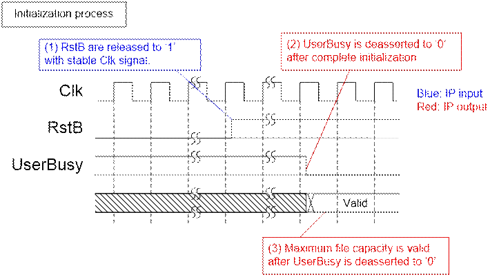
Figure 3: FAT32-IP for NVMe Intialization
User Interface
User interface can be split into two groups, i.e. command interface and data interface. Timing diagram of both groups are compatible to dgIF typeS interface. The input parameters in command interface of FAT32-IP for NVMe are changed from physical level to be file name and numbers of file as shown in Figure 4.
Before sending new command to the IP, UserBusy must be always monitored to confirm that IP is Idle. UserCmd, UserFName, and UserFLen must be valid and latched during asserting UserReq=’1’. UserBusy changes status from ‘0’ to ‘1’ after start the command operation. So, UserReq can be cleared and user logic can prepare the next command to the command bus.
Note: UserFName and UserFLen input are ignored in Format command.
For data interface, transmit FIFO (TXFIFO) is read for Write file command and received FIFO (RXFIFO) is written for Read file command. Timing diagram of data interface are shown in Figure 5 and Figure 6.
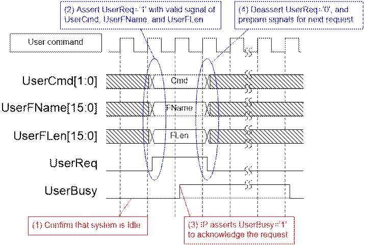
Figure 4: User Interface (Command) Timing diagram
For write command, UserFifoEmpty is monitored to check data available in TXFIFO. When data is ready, UserFifoRdEn is asserted to forward data from TXFIFO to NVMe IP until total data are transferred to NVMe IP. Similar to typical FIFO, UserFifoRdData is valid in the next clock after UserFifoRdEn is asserted, as shown in Figure 5.
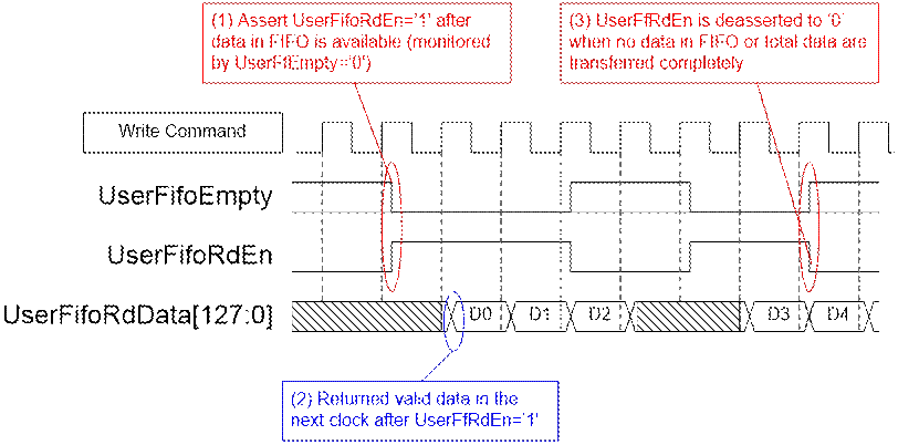
Figure 5: TX FIFO Interface for Write command
For read command, UserFifoWrEn is asserted with the valid value of UserFifoWrData to store data to RXFIFO until total data are transferred to user logic. UserFifoWrCnt is monitored to check the remaining space in the FIFO. Data is transferred when remaining space in FIFO is more than 7 words. If UserFfWrCnt is more than or equal to 65528 (less than 7 words are remaining in FIFO), UserFifoWrEn will be deasserted to ‘0’ to pause data transferring, as shown in Figure 6.
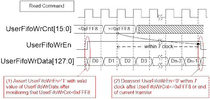
Figure 6: RX FIFO Interface for Read command
Example usage
The example sequence to use FAT32-IP for NVMe to write and read data with NVMe PCIe SSD is shown as follows.
1) Deassert RstB=’1’ to start system initialization. Wait until UserBusy=’0’.
2) Skip to next step when the SSD does not need to format. In case, the SSD needs to format. Send Format command to the IP (UserCmd=”00”). Wait until IP operation complete (UserBusy=’0’).
Note: Format command must be sent from user logic firstly when one of following conditions is matched.
a) The SSD is the new SSD which is not formatted by FAT32-IP for NVMe.
b) User needs to clear data in the SSD.
c) User needs to change a file size parameter.
3) Send Write file command (UserCmd=”10”) or Read file command (UserCmd=”11”) to the SSD. FSize value must not be changed after the SSD is formatted.
In case of write command,
a) Set FDateY, FDateM, FDateD, FTimeH, FTimeM, and FTimeS to set up “Created date” and “Created time” of the file. All values must not be changed during write operation.
b) Send Write file command with a valid UserFName and UserFLen. UserFName must be the next value from the latest file. For example, if the latest file in the SSD is FILE0010.BIN, UserFName will be set to 0x000B to create FILE0011.BIN to be the 1st file in this command. UserFLen value must not be more than (TotalFCap – UserFName).
c) Send total data to TXFIFO and the IP reads the data from TXFIFO by monitoring UserFifoEmpty=’0’. Total data size is equal to UserFLen x FSize.
d) Wait until IP operation complete (UserBusy=’0’).
In case of read command,
a) Send Read file command with valid UserFName and UserFLen. (UserFName + UserFLen) value must not be more than total number of files in the SSD.
b) Read total data from RXFIFO. The IP monitors UserFifoWrCnt[15:3] /= all 1, before sending received data to RXFIFO. Total data size is equal to UserFLen x FSize.
c) Wait until IP operation complete (UserBusy=’0’).
Additional Information
1) FAT32-IP for NVMe calculates FAT32 parameters using in all operations from user inputs and SSD capacity. File system in the SSD is specially designed for using in FAT32-IP for NVMe. So, the SSD must not be formatted or written by other system. Only read file from the SSD is allowed for other system.
2) Physical address of the SSD to store user data in each file is calculated from file name and file size input from user. So FSize input from user must not change when user writes or reads the file with the SSD. User needs to send Format command after user changes FSize input value. TotalFCap is updated when FSize value is changed.
3) For Write file command, UserFName input must be the next value from the latest file name, as shown in Figure 7.
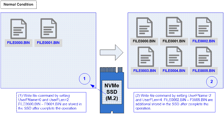
Figure 7: Write file command in normal condition
If UserFName is not equal to the next value, the new file will be created with unusual status. The example of the unusual status is as follows.
a) When UserFName is more than the next value of the latest file, the dummy file which cannot be accessed is created between the latest file and the 1st new file, as shown in Figure 8.
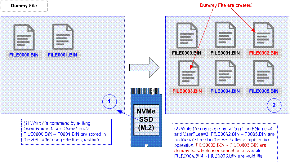
Figure 8: Write file command but UserFName is more than normal value
b) When UesrFName is less than the next value of the latest file, the file after the 1st new file is lost, as shown in Figure 9.
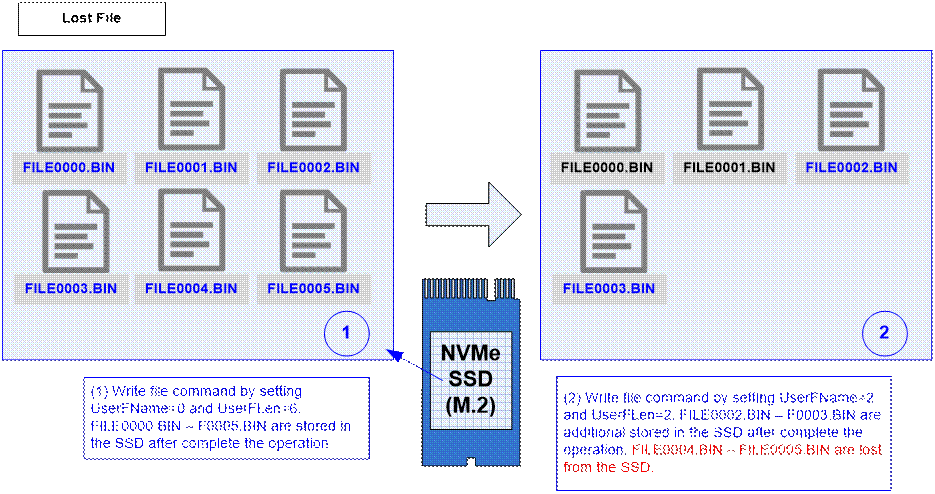
Figure 9: Write file command but UserFName is less than normal value
Verification Methods
The FAT32 IP Core for NVMe functionality was verified by simulation and also proved on real board design by using Arria10 SoC/Arria10 GX development board.
Recommended Design Experience
Experience design engineers with a knowledge of QuartusII Tools should easily integrate this IP into their design.
Ordering Information
This product is available directly from Design Gateway Co., Ltd. Please contact Design Gatway Co., Ltd. for pricing and additional information about this product using the contact information on the front page of this datasheet.
Revision History
|
Revision |
Date |
Description |
|
1.0 |
Nov-8-2017 |
New release |