FAT32-IP for NVMe Demo Instruction
Rev1.0 9-Aug-23
a) Arria10 GX Development board by AB16 and ATX power supply
b) Arria10 SoC Development board by PCIe Female connector
This document describes the instruction to run FAT32-IP for NVMe demo on FPGA development board. AB16-PCIeXOVR board is required to connect NVMe SSD with FPGA board, except some boards which have PCIe female connector. The demo is designed to write and verify data with NVMe PCIe SSD. User can choose test operation through NiosII command shell.
1 Environment Requirement
To demo FAT32-IP for NVMe on IntelFPGA board, please prepare the following hardware/software.
1) IntelFPGA board:
- Arria10 SoC Development board (PCIe Gen3)
- Arria10 GX Development board (PCIe Gen3)
2) PC with QuartusII programmer and NiosII command shell software
3) For Arria10 GX Development board, AB16-PCIeXOVR board and ATX power supply for SSD
4) Power adapter of IntelFPGA board
5) NVMe PCIe SSD
6) A micro USB cable for programming FPGA and for NiosII command shell, connecting between FPGA board and PC.
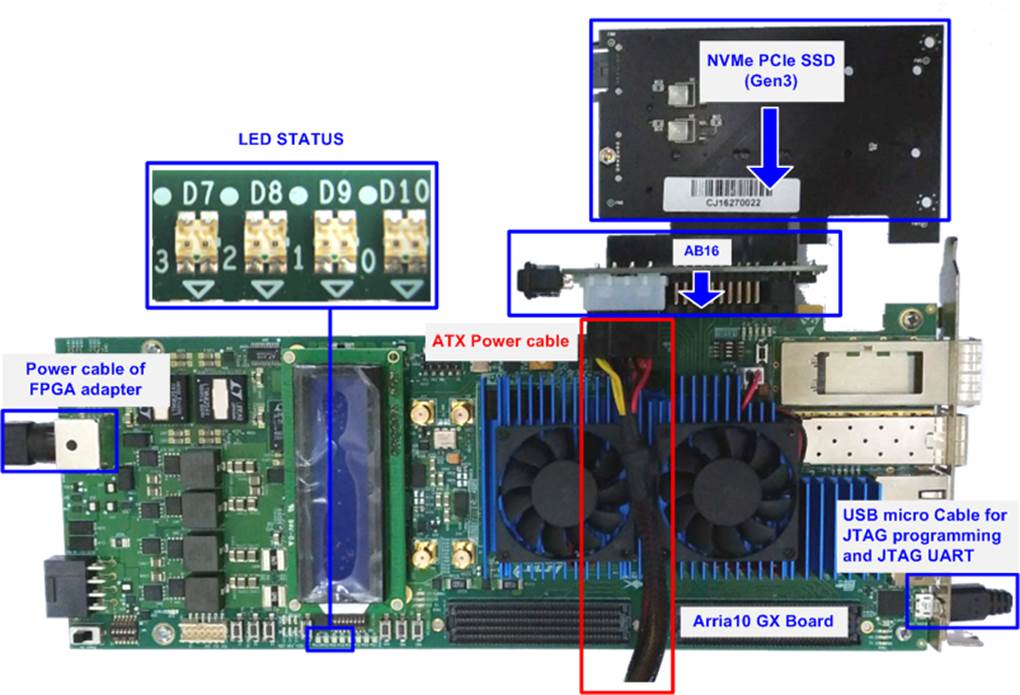
Figure 1‑1 FAT32-IP for NVMe Demo Environment Setup on Arria10 GX Development Board
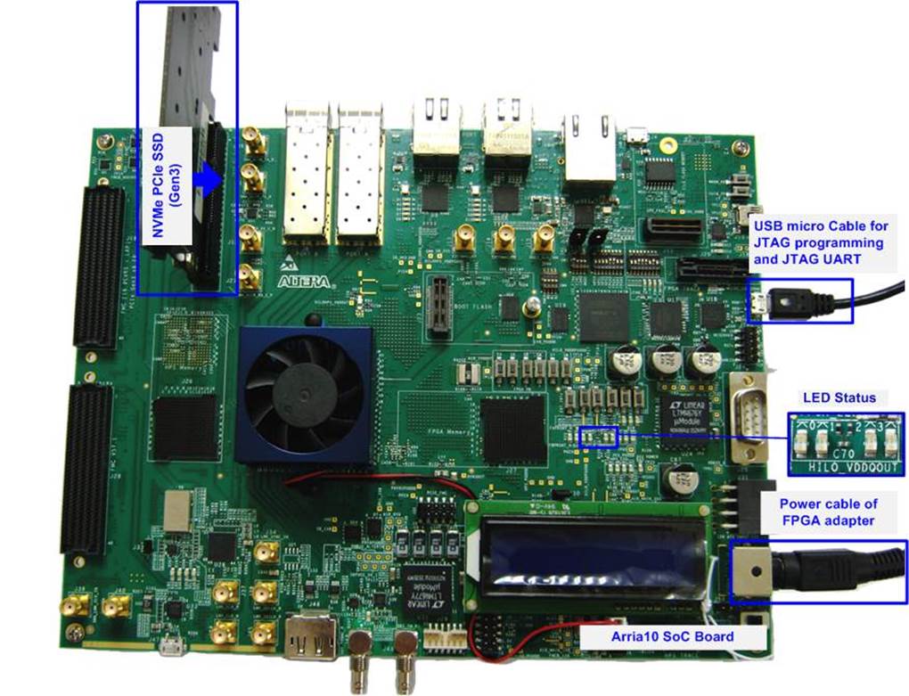
Figure 1‑2 FAT32-IP for NVMe Demo Environment Setup on Arria10 SoC Development Board
2 Demo setup
2.1 PCIe setup
a) Arria10 GX Development board by AB16 and ATX power supply
- Power off system.
- Connect ATX power to ATX power connector on AB16-PCIeXOVR board.
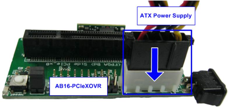
Figure 2‑1 Connect ATX Power to AB16-PCIeXOVR
- Connect A Side of PCIe connector on AB16-PCIeXOVR board to PCIe connector on FPGA board, as shown in Figure 2‑2.
- Check that two mini jumpers are inserted at J5 connector on AB16.
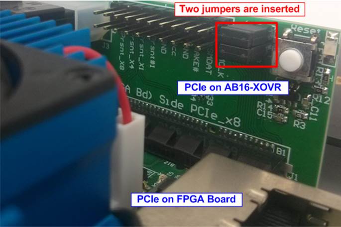
Figure 2‑2 Connect PCIe connector between AB16 and FPGA board
- Connect NVMe PCIe SSD to B Side of PCIe connector on AB16-PCIeXOVR board as shown in Figure 2‑3.
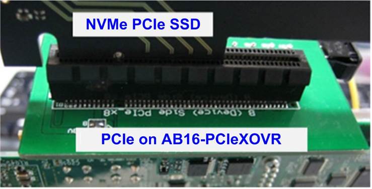
Figure 2‑3 Connect NVMe PCIe SSD to AB16 board
- Connect micro USB cable from FPGA board to PC for JTAG programming and for NiosII command shell.
- Connect FPGA power adapter to FPGA board
- Power on FPGA development board, AB16-PCIeXOVR board, and ATX power supply
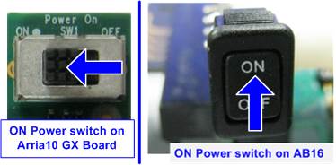
Figure 2‑4 Power on FPGA and AB16 board on Arria10 GX Development board
b) Arria10 SoC Development board by PCIe Female connector
- Power off system.
- Connect NVMe PCIe SSD to PCIe connector on FPGA board, as shown in Figure 2‑5.
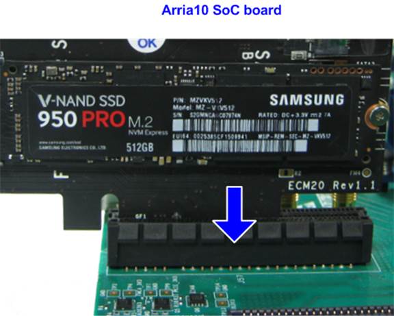
Figure 2‑5 NVMe PCIe SSD connection on FPGA board
- Connect micro USB cable from FPGA board to PC for JTAG programming and for NiosII command shell, as shown in Figure 2‑6.
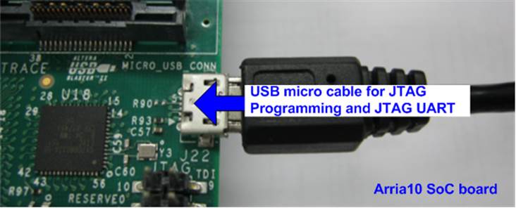
Figure 2‑6 USB cable connection
- set SW1[2] = OFF position to source power to the PCIe, as shown in Figure 2‑7.
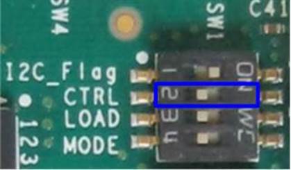
Figure 2‑7 Source power to the PCIe for Arria10 SoC board
- Connect FPGA power adapter to FPGA board, as shown in Figure 2‑8.
- Power on FPGA development board.
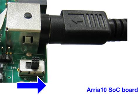
Figure 2‑8 Power on FPGA board
2.2 Board setup
1) Use QuartusII Programmer to program “FAT32NVMeTest.sof” file, as shown in Figure 2‑9.
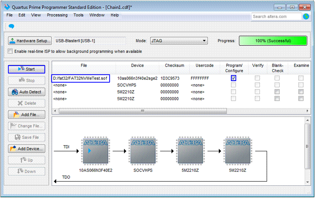
Figure 2‑9 Programmed by QuartusII Programmer
2) Open NiosII Command Shell and run nios2-terminal command. Boot message is displayed. User can set file size by press ‘y’ or ‘Y’. If user refuses to set file size, it will be set to default (32 MB). After that, main menu is displayed on the command shell, as shown in Figure 2‑10 and Figure 2‑11.
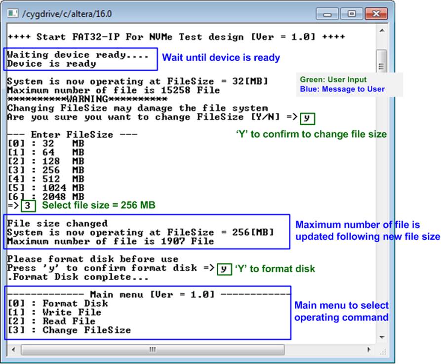
Figure 2‑10 Main menu when confirm to set file size
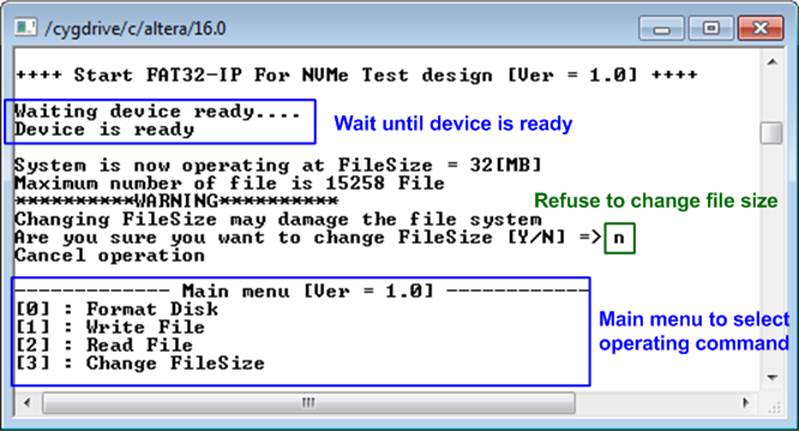
Figure 2‑11 Main menu when skip to set file size
3) Check LED status on FPGA board. The description of LED is shown as follows.
Table 1 LED Definition
|
GPIO LED |
ON |
OFF |
|
0 |
Normal operation |
System is in reset condition |
|
1 |
System is busy |
Idle status |
|
2 |
Error detect |
Normal operation |
|
3 |
Data verification fail |
Normal operation |
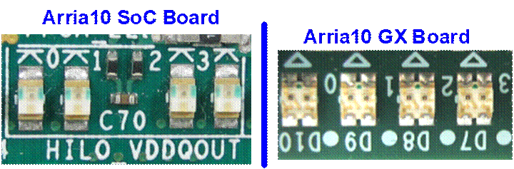
Figure 2‑12 4-bit LED Status for user output
4) After programming completely, LED[0] and LED[1] are ON during FAT32 initialization process. Then, LED[1] is OFF to show that FAT32-IP for NVMe completes initialization process and now system is ready to receive command from user.
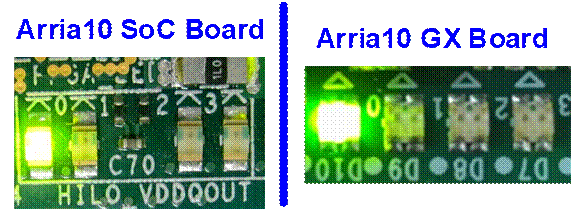
Figure 2‑13 LED status after program configuration file and FAT32-IP initialization complete
3 Test Menu
3.1 Format Disk
Select ‘0’ to send Format disk command to the NVMe SSD. After the operation is completed, the system shows current operation file size and maximum number of file, as shown in Figure 3‑1.
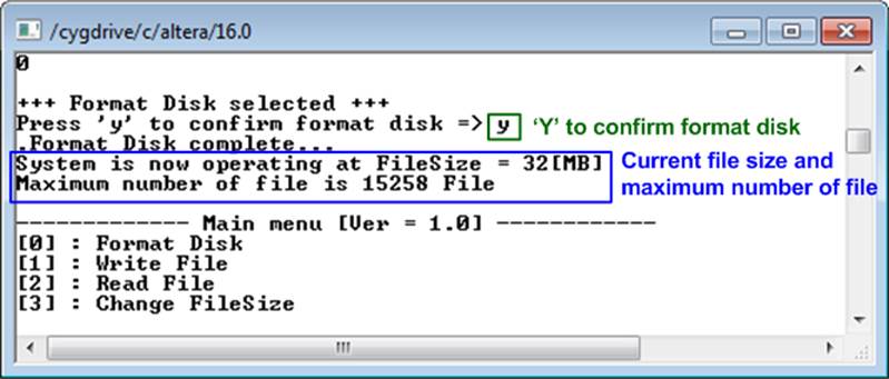
Figure 3‑1 Result from Format Disk menu
3.2 Write File
Select ‘1’ to send Write command to the NVMe SSD. After that, users are asked to set created time of file. Users can input ‘y’ or ‘Y’ to confirm to change created time or input others to refuse. If user choose to refuse, the created time will be set to default (default created time is 22 Sep 2017, 15:31:18).
The details of created time are shown as in Figure 3‑2. Next, users can input created time of file. If input is invalid, the parameter will not change. Only parameter that valid is changed. Then, the new created time is displayed.
After setting created time process is done, user inputs by the following steps.
1) Start file No – Input a number of the first written file. The input can be decimal unit or add prefix “0x” for hexadecimal unit.
2) NUM of file – Input total transfer size in file unit. The input can be decimal unit or add prefix “0x” for hexadecimal unit.
3) Select pattern – Select pattern of test data for writing to device. Five types can be selected, e.g. 32-bit increment, 32-bit decrement, all 0, all 1, and 32-bit LFSR counter.
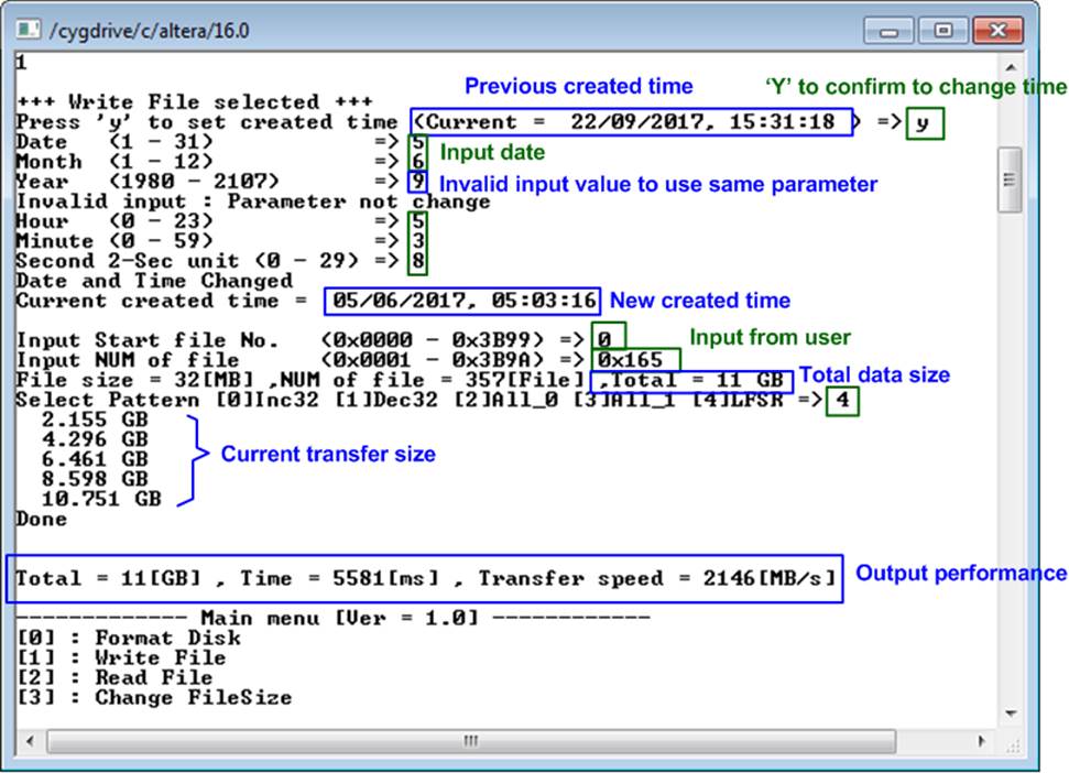
Figure 3‑2 Result from Write File menu when changing created time is confirmed
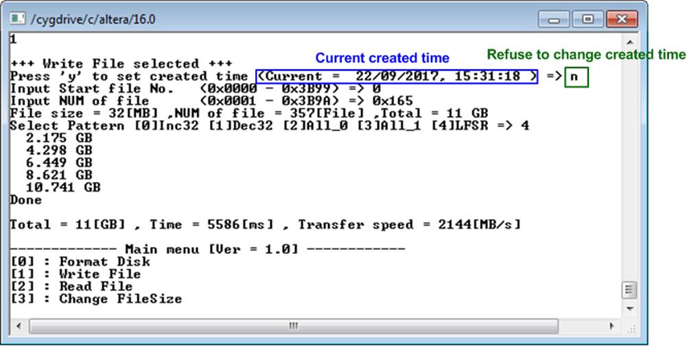
Figure 3‑3 Result from Write File menu when changing created time is refused
As shown in Figure 3‑2 and Figure 3‑3, if all inputs are valid, the operation will be started. Total data size is displayed first. Then, current transfer size is displayed out to the command shell every second during writing operation to show that system still operates. When operation is done, test performance (data written size, time usage, and transfer speed) is displayed on the command shell.
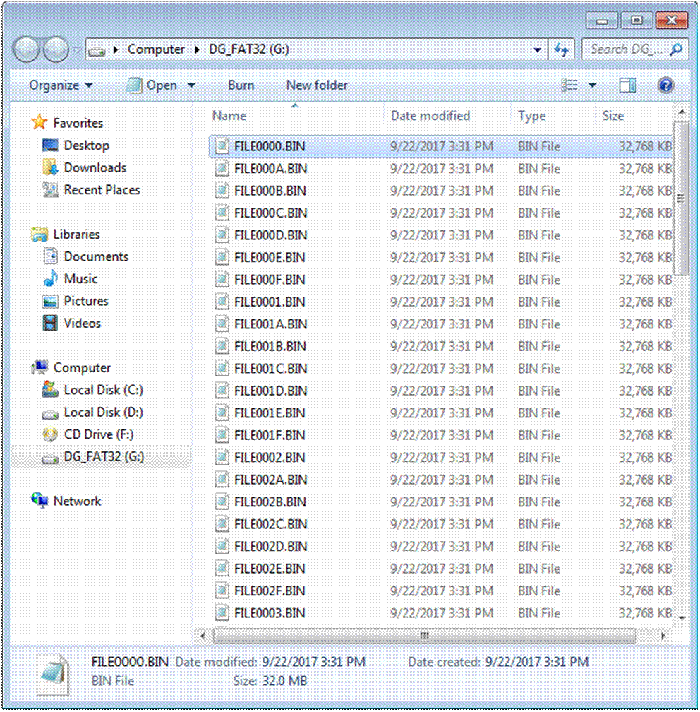
Figure 3‑4 Example test files that written by Write File command
Test data is written to the NVMe SSD as a file with constant file size. The File is named FILExxxx.BIN, when xxxx is a file number in hexadecimal unit, as shown in Figure 3‑4.
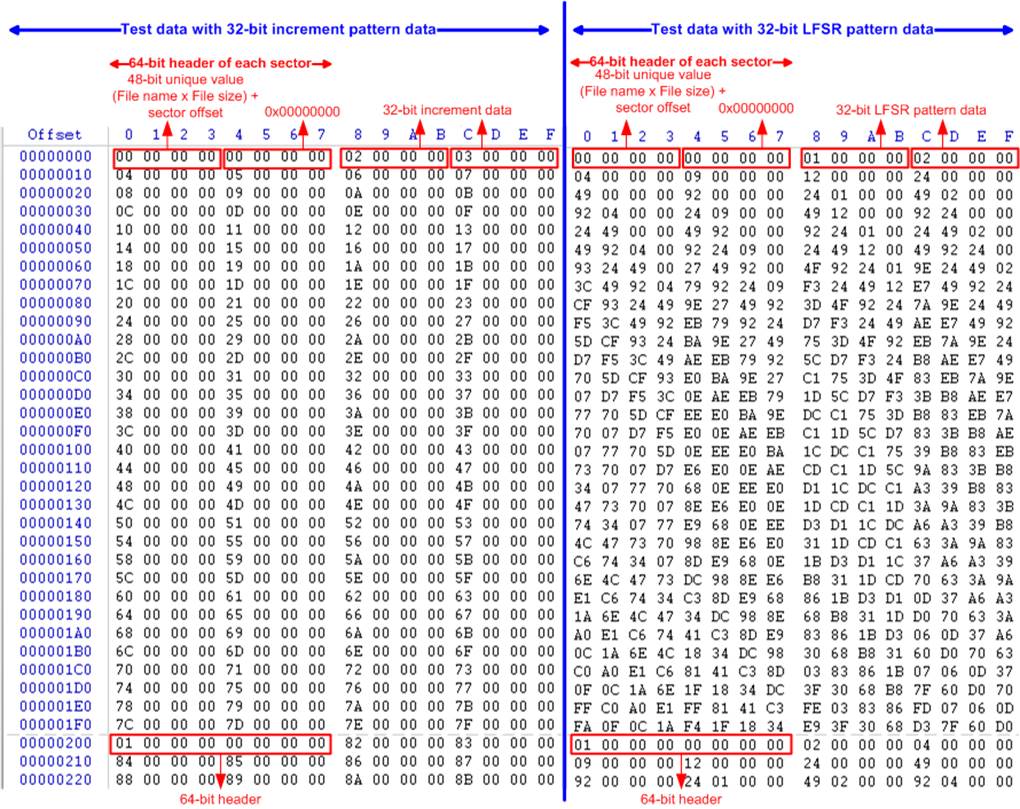
Figure 3‑5 Example Test data in sector#0 - #1 by increment/LFSR pattern
Data in the test file inserts 64-bit header every 512-byte. The header is unique value in one NVMe SSD. The first 32-bit header is calculated by (file name x file size) + sector offset in the file. The remaining 32-bit data is 0. After that, the test pattern is filled following user selection such as 32-bit increment pattern (left window of Figure 3‑5) and 32-bit LFSR pattern (right window of Figure 3‑5).
Figure 3‑6 – Figure 3‑8 show error messages when user’s input is invalid. “Invalid input” message is displayed on the command shell, and then returns to main menu to receive new command.
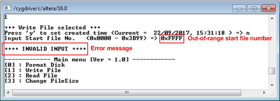
Figure 3‑6 Invalid start file number input
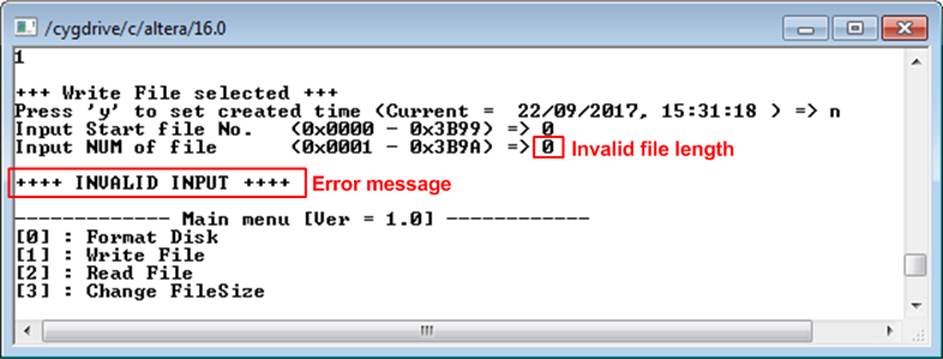
Figure 3‑7 Invalid file length input
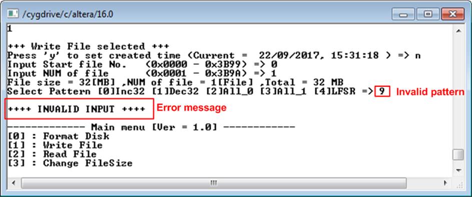
Figure 3‑8 Invalid pattern input
3.3 Read File
Select ‘2’ to read file to the NVMe SSD. Three inputs are required for this menu.
1) Start file No – Input a number of the first read file. The input can be decimal unit or add prefix “0x” for hexadecimal unit.
2) NUM of file – Input total transfer size in file unit. The input can be decimal unit or add prefix “0x” for hexadecimal unit.
3) Select pattern – Select pattern to verify data from device. Test pattern must be matched with written data. Five types can be selected, e.g. 32-bit increment, 32-bit decrement, all 0, all 1, and 32-bit LFSR counter.
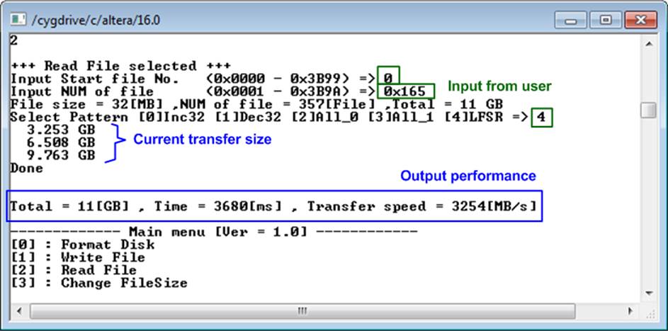
Figure 3‑9 Result and input from Read File menu with successful verification
Similar to write test, if all inputs are valid, the operation will be started. Total data size is displayed first. Then, current transfer size is displayed out to the console every second during reading operation to show that system still operates. Final stage, test performance is displayed when the transfer is done. “Invalid input” will be displayed if any inputs are invalid.
Figure 3‑10 and Figure 3‑11 show the error message when data verification is failed. “Verify fail” message is displayed with name of the first file that error occurs, error address, expected data, and read data. User can press any keys to cancel the operation or wait until all read process complete.
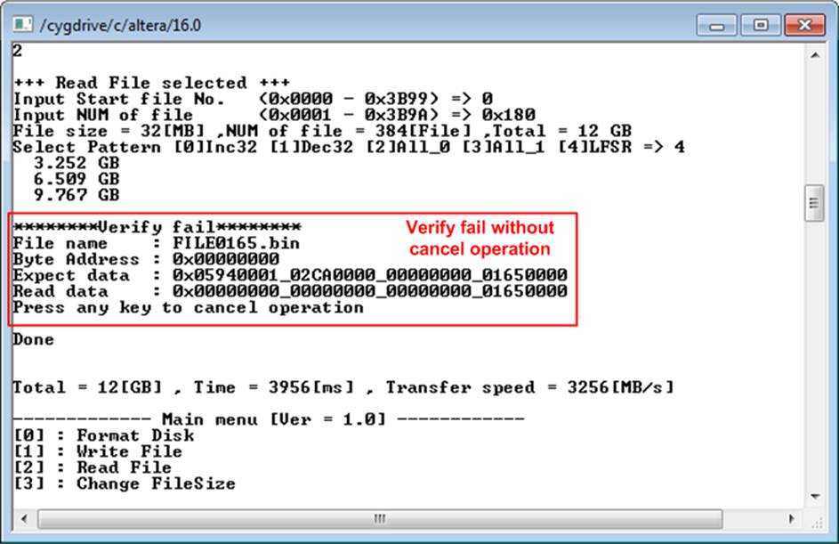
Figure 3‑10 Data verification is failed and user does not cancel operation
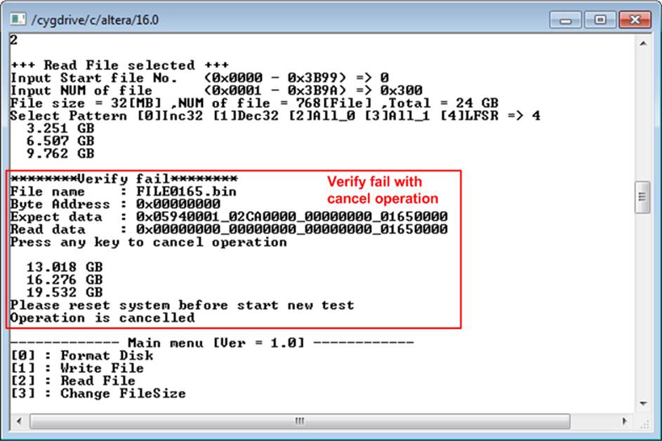
Figure 3‑11 Data verification is failed and user cancels operation
3.4 Change File Size
Select ‘3’ to change file size. After selecting menu, current file size and warning message are displayed on the console. Then, user can input ‘y’ or ‘Y’ to confirm to change file size or input others to cancel the operation.
After confirming to change file size, the selecting file size menu is displayed. User can select the new file size here. When changing file size is completed, the system updates current operating file size and maximum file number.
When file size is changed, a request to format disk message is asked. Then, user can input ‘y’ or ‘Y’ to accept format disk operation or input others to refuse.
Note: Changing file size may damage to the file system. Therefore, user should format disk after the operation to delete files in the device.
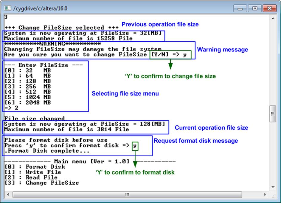
Figure 3‑12 Result from Change FileSize command
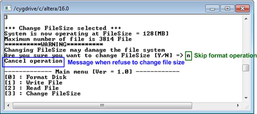
Figure 3‑13 Cancel Change FileSize command
4 Revision History
|
Revision |
Date |
Description |
|
1.0 |
8-Nov-17 |
Initial version release |