FAT32-IP for NVMe reference design manual
Rev1.0 3-Jul-23
1. Introduction
In the hardware system, data stream can be stored to the SSD by using raw data or file system. Using raw data, the data is allocated in the SSD through physical address. If there are many data types in one SSD, the user will need to assign different address for each data group. The disadvantage of raw data is the new users who do not know the memory map of data group in the SSD. Therefore, they cannot understand the data in the SSD and which area is available to write the additional data.
As a result, file system is created to manage data in the SSD by setting up the table to be an index for data that is written to the SSD. The data is separated into many groups. Each group is called a “file”. For system flexibility, one file has some information to represent itself such as file name, file type, file size, and physical address of data in the file. So, the user can search the data to read from the SSD and can identify where the free space in the SSD available to write new data.
FAT32 is one of the most popular file systems to use in the storage device and file structure is not complicated to build by pure logic. The limitation of FAT32 is maximum partition size is 2 TB and maximum file size is 4 GB.
Generally, when the system accesses the data in the SSD through file system, the data transfer speed is lower than raw data. To access file system, it has the overhead time to read the file structure to know the physical address of the data in each file. Also, sometimes the data in one file is split into many parts which store in different physical address. Using file system makes the system more convenient and more flexible, but the performance to write or read the data is reduced, comparing to raw data.
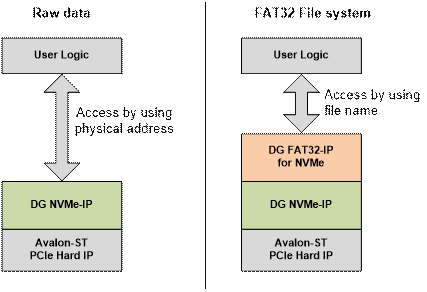
Figure 1‑1 Hardware system for Raw data and File system
DG FAT32-IP for NVMe implements FAT32 file system by pure-hardware logic which achieve same write and read speed similar to raw data system. As shown in Figure 1‑1, raw data system is designed by connecting DG NVMe-IP and Avalon-ST PCIe Hard IP to transfer ultra high speed data with NVMe SSD. The user interface to access the data of DG NVMe-IP is physical address.
In order to use FAT32 file system, DG FAT32-IP for NVMe is additional block to interface between user logic and DG NVMe-IP. Instead of using physical address, user can access the data in NVMe SSD by using file name.
More details of FAT32-IP for NVMe reference design are described in the next topic.
2. Hardware overview
The reference design of DG FAT32-IP for NVMe is modified from NVMe-IP reference design by adding DG FAT32-IP to NVMe-IP block, as shown in Figure 2‑1.
Please see more details of NVMe-IP reference design from following document.
http://www.dgway.com/products/IP/NVMe-IP/dg_nvmeip_refdesign_intel_en.pdf
http://www.dgway.com/products/IP/NVMe-IP/dg_nvmeip_instruction_intel_en.pdf
This document describes the modification part from NVMe-IP reference design.
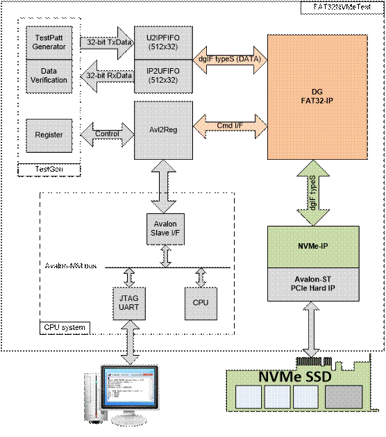
Figure 2‑1 FAT32-IP for NVMe Demo System
Comparing to NVMe-IP reference design, the command interface of DG FAT32-IP is file name and numbers of file instead of physical address and length. Data path of DG FAT32-IP still uses dgIF typeS interface. So, TestGen and two FIFOs in test module are almost similar to NVMe-IP reference design. Register map within Avl2Reg module is modified to change the parameters from physical layer to be file system.
CPU firmware is designed to receive user command through JTAG UART. There are three menus for three commands, i.e. format, write file, and read file. Transfer performance by using FAT32-IP for NVMe is same as performance by using NVMe-IP. The final performance in the demo depends on the limitation of NVMe SSD.
3. CPU
CPU system in FAT32 for NVMe demo is same as NVMe-IP reference design. But register map for user interface is changed from physical address for raw data access to be file system parameters for file system access. More details are shown in Table 1.
The details of FAT32-IP for NVMe signals are described in the datasheet.
http://www.dgway.com/products/IP/NVMe-IP/dg_nvmeip_datasheet_intel_en.pdf
Table 1 Register Map
|
Address |
Register Name |
Description |
|
Rd/Wr |
(Label in the “fat32nvmetest.c”) |
|
|
BA+0x00 |
User File Name Reg |
[15:0]: Input to be UserFName of FAT32-IP for NVMe |
|
Wr |
(USERFNAME_REG) |
|
|
BA+0x04 |
User File Length Reg |
[15:0]: Input to be UserFLen of FAT32-IP for NVMe |
|
Wr |
(USERFLEN_REG) |
|
|
BA+0x08 |
File Size Reg |
[2:0]: Input to be FSize of FAT32-IP for NVMe |
|
Wr |
(FSIZE_REG) |
|
|
BA+0x0C |
File Time Reg |
[4:0]: Input to be FTimeS of FAT32-IP for NVMe [10:5]: Input to be FTimeM of FAT32-IP for NVMe [15:11]: Input to be FTimeH of FAT32-IP for NVMe [20:16]: Input to be FDateD of FAT32-IP for NVMe [24:21]: Input to be FDateM of FAT32-IP for NVMe [31:25]: Input to be FDateY of FAT32-IP for NVMe |
|
Wr |
(DATETIME_REG) |
|
|
BA+0x10 |
User Command Reg |
[1:0]: Input to be UserCmd of FAT32-IP for NVMe When this register is written, the design generates UserReq (command request) to FAT32-IP for NVMe to start new command operation. |
|
Wr |
(USERCMD_REG) |
|
|
BA+0x14 |
Pattern Select Reg |
[2:0]: Test pattern select “000”-Increment, “001”-Decrement, “010”-All 0, “011”-All 1, “100”-LFSR |
|
Wr |
(PATTSEL_REG) |
|
|
BA+0x1C |
User Reset Reg |
[0]: ‘1’-Reset test system, ‘0’-Release reset |
|
Wr |
(RESET_REG) |
|
|
BA+0x100 |
User Status Reg |
[0]: Mapped to UserBusy of FAT32-IP for NVMe [1]: Mapped to UserError of FAT32-IP for NVMe [2]: Data verification fail (‘0’: Normal, ‘1’: Error) |
|
Rd |
(USRSTS_REG) |
|
|
BA+0x104 |
Total file capacity Reg |
[15:0]: Mapped to TotalFCap of FAT32-IP for NVMe |
|
Rd |
(TOTALFCAP_REG) |
|
|
BA+0x108 |
User Error Type Reg |
[31:0]: Mapped to UserErrorType of FAT32-IP for NVMe |
|
Rd |
(USRERRTYPE_REG) |
|
|
BA+0x10C |
FAT32-IP Test pin (Low) Reg |
[31:0]: Mapped to TestPin[31:0] of FAT32-IP for NVMe |
|
Rd |
(FATTESTPINL_REG) |
|
|
BA+0x110 |
FAT32-IP Test pin (High) Reg |
[31:0]: Mapped to TestPin[63:32] of FAT32-IP for NVMe |
|
Rd |
(FATTESTPINH_REG) |
|
|
BA+0x14C |
NVMe Completion Status Reg |
[15:0]: Mapped to AdmCompStatus[15:0] of NVMe-IP [31:16]: Mapped to IOCompStatus[15:0] of NVMe-IP |
|
Rd |
(COMPSTS_REG) |
|
|
BA+0x150 |
NVMe CAP Reg |
[31:0]: Mapped to NVMeCAPReg[31:0] of NVMe-IP |
|
Rd |
(NVMCAP_REG) |
|
|
BA+0x154 |
NVMe-IP Test pin Reg |
[31:0]: Mapped to TestPin[31:0] of NVMe-IP |
|
Rd |
(NVMTESTPIN_REG) |
|
|
BA+0x180 |
Failure Byte Address Reg |
[31:0]: Failure data address in the file |
|
Rd |
(FAILADDR_REG) |
|
|
BA+0x184 |
Failure File Name Reg |
[15:0]: Failure file name |
|
Rd |
(FAILFNAME_REG) |
|
|
BA+0x188 |
Expected value Word0 Reg |
[31:0]: Expected data [31:0] of failure address. |
|
Rd |
(EXPPATW0_REG) |
|
|
BA+0x18C |
Expected value Word1 Reg |
[31:0]: Expected data [63:32] of failure address. |
|
Rd |
(EXPPATW1_REG) |
|
|
BA+0x190 |
Expected value Word2 Reg |
[31:0]: Expected data [95:64] of failure address. |
|
Rd |
(EXPPATW2_REG) |
|
|
BA+0x194 |
Expected value Word3 Reg |
[31:0]: Expected data [127:96] of failure address. |
|
Rd |
(EXPPATW3_REG) |
|
Address |
Register Name |
Description |
|
Rd/Wr |
(Label in the “fat32nvmetest.c”) |
|
|
BA+0x198 |
Read value Word0 Reg |
[31:0]: Read data [31:0] of failure address. |
|
Rd |
(RDPATW0_REG) |
|
|
BA+0x19C |
Read value Word1 Reg |
[31:0]: Read data [63:32] of failure address. |
|
Rd |
(RDPATW1_REG) |
|
|
BA+0x1A0 |
Read value Word2 Reg |
[31:0]: Read data [95:64] of failure address. |
|
Rd |
(RDPATW2_REG) |
|
|
BA+0x1A4 |
Read value Word3 Reg |
[31:0]: Read data [127:96] of failure address. |
|
Rd |
(RDPATW3_REG) |
|
|
BA+0x1A8 |
Current test byte (Low) Reg |
[31:0]: Current test data size of TestGen module in byte unit (bit[31:0])
|
|
Rd |
(CURTESTSIZEL_REG) |
|
|
BA+0x1AC |
Current test byte (High) Reg |
[7:0]: Current test data size of TestGen module in byte unit (bit[39:32])
|
|
Rd |
(CURTESTSIZEH_REG) |
CPU firmware is designed to control and set parameters to user interface of FAT32-IP for NVMe. The parameters are received from user through JTAG UART. CPU firmware sequences are described as follows.
3.1 Initialization
1) After system boot up, CPU monitors UserBusy flag (USRSTS_REG[0]). CPU waits until FAT32-IP for NVMe completes initialization sequence (UserBusy=’0’).
2) CPU displays maximum numbers of file which can store in the SSD by reading TOTALFCAP_REG. This value is calculated by setting file size to be 32 MB (FSIZE_REG=”000). User can select “Change file size” menu to update usage file size and TOTALFCAP_REG.
3) Go to main menu to wait the new command from user.
3.2 Format
1) Set USERCMD_REG=”00” to format the SSD. UserReq is asserted to ‘1’ to start the operation. UserBusy is asserted to ‘1’ by FAT32-IP during formatting.
2) CPU monitors UserBusy flag (USRSTS_REG[0]). CPU goes to next step when UserBusy is de-asserted to ‘0’ (operation is completed) or UserError flag (USRSTS_REG[1]) is asserted to ‘1’.
3) If the operation is completed without error, CPU will display maximum numbers of file which can store in the SSD (TOTALFCAP_REG) to the NiosII terminal.
If the error is found, error message will be displayed instead.
3.3 Write file or read file
1) Receive the parameters from user (the 1st File name, total numbers of file to transfer, and test pattern format) through the NiosII terminal. If some inputs are invalid, the operation will be cancelled.
In case of write file operation, user can select to change created date and time of the file or use current value. The created date and time value are set to DATETIME_REG.
2) Set the inputs from user to internal registers (USERFNAME_REG, USERFLEN_REG, and PATTSEL_REG). After that, CPU sets USERCMD_REG=”10” or “11” to start write file or read file operation.
3) During operating, CPU displays total transfer size (CURTESTSIZE_REG) to the NiosII terminal every second.
In case of read file operation, Data failed flag (USRSTS_REG[2]) is monitored. If data failed flag is asserted to ‘1’, warning message will show failure data position (FAILADDR, FILENAME), expected test data (EXPPATW0_REG to EXPPATW3_REG), and read data (RDPATW0_REG to RDPATW3_REG) to the NiosII terminal. User can press any keys to cancel the operation.
4) The operation is stopped when UserBusy is de-asserted to ‘0’ (operation is completed) or UserError flag (USRSTS_REG[1]) is asserted to ‘1’.
If operation is completed, total transfer speed will be displayed on the NiosII terminal.
If the error is found, error message will be displayed instead.
3.4 Change File size
1) Receive new file size value from user through NiosII terminal. If the input is valid and UserBusy=’0’, the new value will be set to FSIZE_REG.
2) CPU displays maximum numbers of file which can store in the SSD by reading TOTALFCAP_REG. Warning message is also displayed to format the SSD when file size is changed.
4. Avl2Reg and TestGen
Hardware block of both modules are almost similar to NVMe-IP reference design. Please see more details of NVMe-IP reference design.
The different point of Avl2Reg in NVMe-IP and Avl2Reg in FAT32 for NVMe demo is the register map of UserReg module inside Avl2Reg. The new register is mapped following Table 1.
TestGen is modified to compatible with FAT32-IP for NVMe interface. User Interface are file name, file size and numbers of file instead of physical address and length. And data verification of TestGen module is modified to indicate error in file number unit instead of physical byte address unit.
5. Example Test Result
The example test result when running demo system by using 512 GB Samsung 960 Pro is shown in Figure 5‑1.
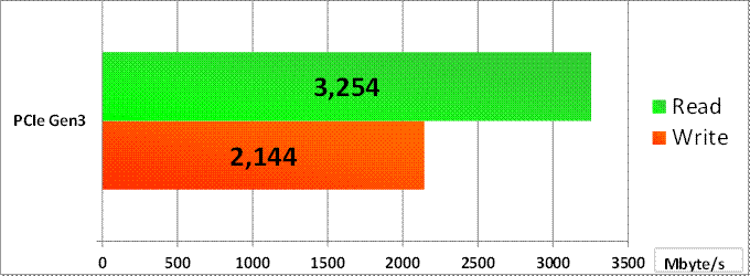
Figure 5‑1 Test Performance of FAT32-IP demo by using Samsung 960 Pro SSD
By using PCIe Gen3 on Arria10 SoC board, write performance is about 2144 Mbyte/sec and read performance is about 3254 Mbyte/sec.
6. Revision History
|
Revision |
Date |
Description |
|
1.0 |
8-Nov-17 |
Initial Release |
Copyright: 2017 Design Gateway Co,Ltd.