muNVMe-IP for Gen4 reference design manual
Rev1.1 8-Aug-23
2.2.2 PCIe Hard IP (P-Tile/F-Tile Avalon-ST Intel FPGA for PCIe)
3.1 Test firmware (munvmeiptest.c)
3.2 Function list in Test firmware
1 Overview
NVMe-IP for Gen4 has one user interface for sending one command in each time. The next command can be requested after the first command is done. Therefore, user cannot send Write and Read command to access two areas of the same SSD at the same time. To be the solution, muNVMe-IP for Gen4 (multiple-user NVMe-IP for Gen4) is designed to have four user interfaces for sending up to four Write/Read commands to the same SSD at the same time.
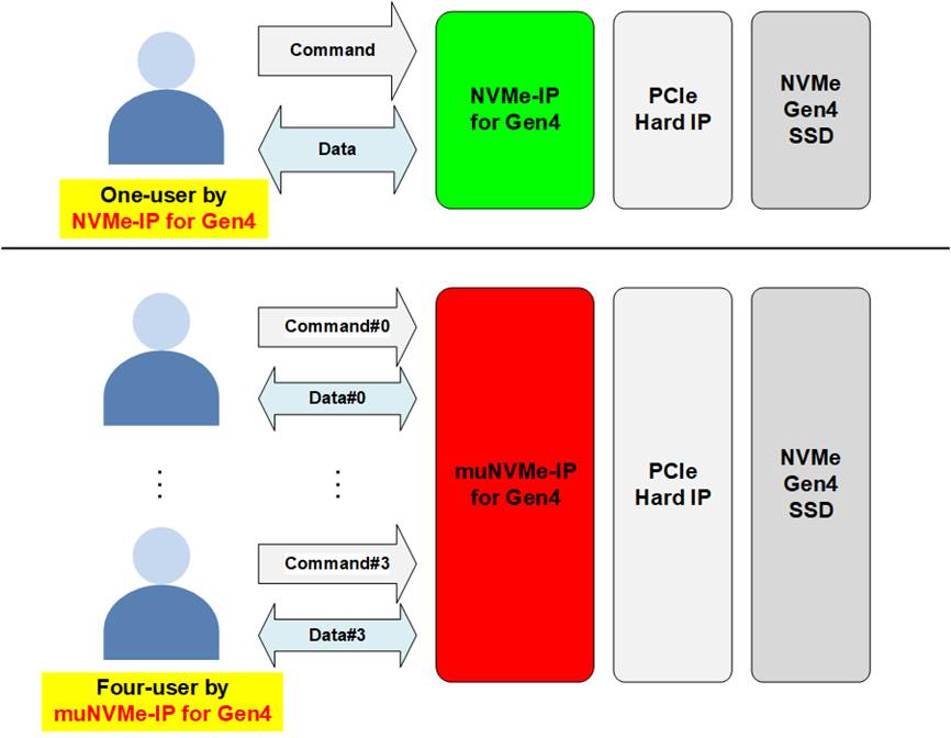
Figure 1‑1 NVMe-IP for Gen4 and muNVMe-IP for Gen4 comparison
The number of user interfaces can be configured to be 2, 3, or 4 by assigning the parameters on HDL code to the muNVMe-IP for Gen4. Similarly, the user can configure the buffer size inside muNVMe-IP for Gen4 by assigning the parameters on HDL code. The FPGA resource utilization is reduced when using smaller buffer size and smaller number of user interfaces. The command value for each user interface can be requested individually. Therefore, the user can send the same command or the different command for all user interfaces such as four Write commands, four Read commands, two Write and two Read commands. When all interfaces run the same command, the write performance or the read performance of each user interface is about the maximum performance when using one user interface divided by four. While running the mixed Write-Read command, the performance depends on the SSD characteristic.
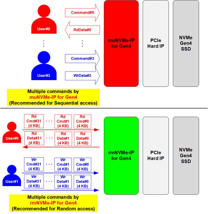
Figure 1‑2 muNVMe-IP for Gen4 and rmNVMe-IP for Gen4 comparison
Design Gateway has another IP solution, called rmNVMe-IP, that has two user interfaces. The Read command can be requested by User#0 interface while the Write command can be requested by User#1 interface. rmNVMe-IP is designed to support random access by fixed the data size of each command to 4 Kbyte. It also supports Write and Read command at the same time. It is fit to the application that requires the random access. While muNVMe-IP is fit to the application that supports sequential Write and Read command to achieve the higher performance than random access.
2 Hardware overview
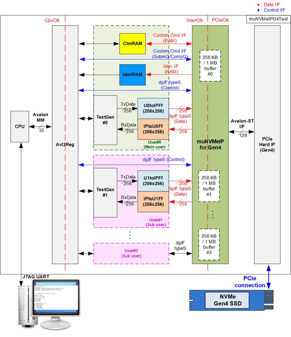
Figure 2‑1 muNVMe-IP for gen4 demo hardware
This reference design configures muNVMe-IP for Gen4 to have four user interfaces. Two configuration files are provided to show the test result when each user inside muNVMe-IP uses 256 KB buffer and 1 MB buffer. Most SSDs show the better Write/Read performance when using 1 MB buffer.
The block diagram in Figure 2‑1 shows the details of the submodule in the reference design. The submodule can be grouped to several groups following the function. First is the test function that consists of TestGen which connects to the user interface of muNVMe-IP. Second is the NVMe function that consists of CtmRAM, IdenRAM, U0-U3toIPFf, IPtoU0-U3Ff, muNVMe-IP for Gen4, and PCIe Hard IP which handle NVMe and PCIe protocol. Last is the CPU system that consists of CPU and Avl2Reg for receiving test parameters from user and displaying the test result to user. In real system, CPU system can be removed and then integrates simple logic to assign test parameters.
TestGen is the test logic to generate test data stream for muNVMe-IP via U0-U3toIPFf when running Write command and read data stream output from muNVMe-IP via IPtoU0-U3Ff for verification when running Read command. Each TestGen module connect with one user interface of muNVMe-IP for Gen4, so four TestGen modules are integrated and run individually. User can assign maximum data rate that transfers in Write/Read command of each TestGen in the test environment.
NVMe includes the muNVMe-IP and the PCIe hard IP (P-Tile/F-Tile Avalon-ST Intel FPGA for PCIe) for accessing NVMe Gen4 SSD directly without PCIe switch. CtmRAM and IdenRAM are included to store the health data from SMART command and the SSD information from Identify command, respectively. Two FIFOs of each user interface (UtoIFFf and IPtoUFf) are applied to show the example data interface of muNVMe-IP for simple control logic.
CPU and Avl2Reg are designed to interface with user via JTAG UART. User can set command and the test parameters on the console. Also, the current status of the test hardware can be monitored on the console. The CPU firmware is implemented to show the example step for running each command on four user interfaces.
There are three clock domains displayed in Figure 2‑1, i.e., CpuClk, UserClk, and PCIeClk. CpuClk is the clock domain of CPU system and its peripherals. This clock must be stable clock and can be different domain from other hardwares. UserClk is the user clock domain for running the user interface of muNVMe-IP, RAM, FIFO, and TestGen. According to muNVMe-IP datasheet, clock frequency of UserClk must be more than or equal to a half of PCIeClk frequency. PCIeClk is the clock output from PCIe hard IP to synchronous with data stream of Avalon-ST interface. This reference design configures the interface to be four of 4-lane PCIe Gen4 at 500 MHz. Therefore, PCIeClk is equal to 500 MHz while UserClk is set to 350 MHz which is more than 250 MHz.
Note: When running with very high-performance SSD, it is found that using UserClk at 350 MHz shows about 5% better performance than using UserClk at 250 MHz. There is more latency time for transferring some control data in specific condition when using slower UserClk frequency.
More details of the hardware are described as follows.
2.1 TestGen
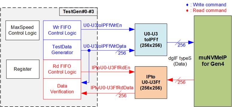
Figure 2‑2 TestGen interface
TestGen module handles the data interface of muNVMe-IP for transferring the data in Write and Read command. In Write command, TestGen sends 256-bit test data to muNVMe-IP via U0-U3toIPFf. In Read command, the test data from TestGen is fed from IPtoU0-U3Ff to compare with the expected value for data verification.
There is MaxSpeed Control Logic in this block which generates enable pulse for controlling the number of clock cycles to assert ‘1’ in every 100 clock cycles. This enable pulse is fed to both Wr and Rd FIFO Control Logic to control the maximum data rate for transferring the data in Write/Read command. The Wr and Rd FIFO Control Logic asserts the write enable and the read enable when the FIFO is ready and the enable pulse from MaxSpeed Control Logic is asserted.
Register file in the TestGen receives test parameters from user, i.e., total transfer size, transfer direction, verification enable, test pattern selector, and Transfer rate. The details of hardware logic of TestGen are shown in Figure 2‑3.
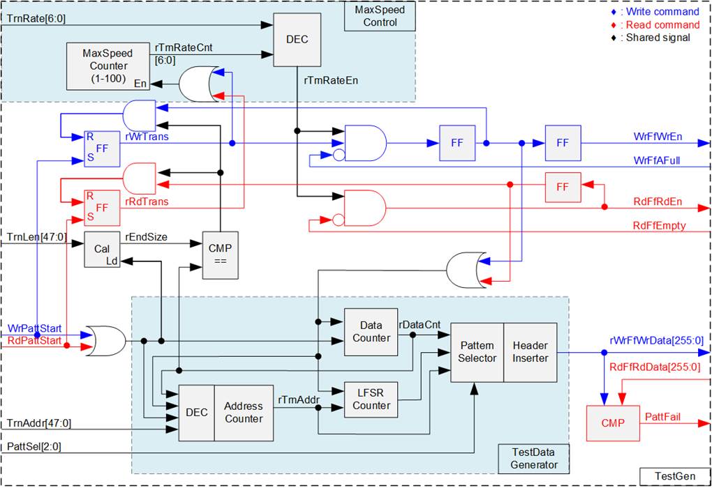
Figure 2‑3 TestGen hardware
MaxSpeed Control Logic is designed by using a counter – MaxSpeed Counter and a decoder to assert rTrnRateEn to ‘1’. The number of cycles that asserts rTrnRateEn to ‘1’ in every 100 clock cycles is set by TrnRate input. The Counter is run while running Write or Read command (rWrTrans=’1’ or rRdTrans=’1’). By monitoring rTrnRateCnt, rTrnRateEn can be asserted to ‘1’ and de-asserted to ‘0’ in specific time to control the maximum data rate. The enable to Write and Read FIFO are asserted only when rTrnRateEn is asserted to ‘1’.
The main flow control signal for Write command and Read command is WrFfAFull and RdFfEmpty, respectively. For Write command, WrFfAFull is de-asserted to ‘0’ when free space in Write FIFO is more than the threshold. WrFfWrEn is asserted to ‘1’ to send Write data to FIFO when WrFfAFull=‘0’ and rTrnRateEn=’1’. For Read command, RdFfEmpty is de-asserted to ‘0’ when there is data available in Read FIFO. RdFfRdEn is asserted to ‘1’ to read data from FIFO when RdFfEmpty=’0’ and rTrnRateEn=’1’.
Four test parameters can be set by the user, i.e., total transfer size (TrnLen), start address (TrnAddr), test pattern selector (PattSel), and transfer rate (TrnRate). TrnLen is fed to the calculating unit to find the end position (rEndSize) for comparing with the Data counter.
TestData Generator has the data counter to count the amount of transferred data (rDataCnt). When the data count is equal to rEndSize, the write enable (rWrTrans) is de-asserted to ‘0’ to stop writing data to FIFO. To generate test data for sending or verifying, user can select five patterns (controlled by PattSel) - all zero, all one, 32-bit incremental data, 32-bit decremental data, and LFSR. All zero and all one pattern are designed by using constant value. While other patterns are designed by separating the data into two parts – 64-bit header and 504-byte test data for creating unique test data in every 512-byte data, as shown in Figure 2‑4.
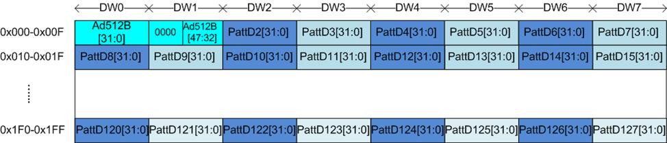
Figure 2‑4 Test pattern format in each 512-byte data for Increment/Decrement/LFSR pattern
64-bit header is assigned in Dword#0 and Dword#1 while the test data is assigned in the remaining words (Dword#2 – Dword#127). The header is created by using the address in 512-byte unit (rTrnAddr), output from the Address counter. The address counter loads the initial value from user (TrnAddr) and then increases its value after finishing 512-byte data transferring. While three different test patterns are designed by using different counter. 32-bit incremental data is designed by using the lower bits of the Data counter. The decremental data uses NOT logic to convert the incremental data to be decremental data. The LFSR pattern uses LFSR counter which is designed by the following equation: x^31 + x^21 + x + 1.
To implement 256-bit LFSR pattern, the data is split to be two sets of 128-bit data with assigning different initial value. Each 128-bit data uses look-ahead technique to calculate four 32-bit LFSR data in one clock cycle. As shown Figure 2‑5, the initial value of LFSR is designed by mixing a part of 32-bit LBA address (LBAAddr) with a part of NOT logic of 32-bit LBA address (LBAAddrB).
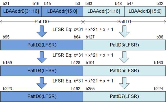
Figure 2‑5 256-bit LFSR Pattern in TestGen
Test data is fed to be write data to the FIFO (rWrFfWrData) in Write command. Also, it is applied to be the expected data for verifying with the read data from FIFO (RdFfRdData). If verification is failed, fail flag (PattFail) is asserted to ‘1’.
The timing diagram when running Write command is shown as follows.
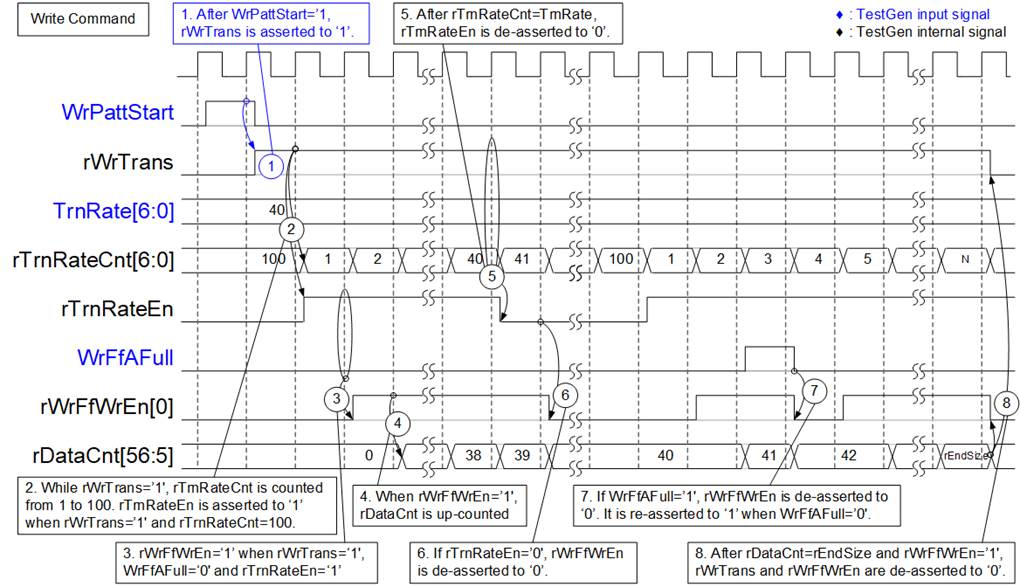
Figure 2‑6 Timing diagram of Write command in TestGen
1) The operation is started when WrPattStart is asserted to ‘1’. This signal is asserted only one clock cycle. After that, rWrTrans is asserted to ‘1’ to show the status that Write request is in operating. It is de-asserted when finishing the operation.
2) While rWrTrans is asserted to ‘1’, rTrnRateCnt is up-counted from 1 to 100. The initial value of rTrnRateCnt is 100. rTrnRateEn is asserted to ‘1’ if rWrTrans=’1’ and rTrnRateCnt=100.
3) When both rWrTrans and rTrnRateEn are asserted to ‘1’ and FIFO is not full (WrFfAFull=’0’), rWrFfWrEn is asserted to ‘1’ to write the test data to FIFO.
4) The data counter (rDataCnt) is up-counted when rWrFfWrEn is asserted to ‘1’. Therefore, it can be monitored to check the total amount of transmitted data to FIFO.
5) This example sets TrnRate=40, so the maximum data rate is about 40/100 = 40% of maximum throughput of this logic. rTrnRateEn is asserted to ‘1’ for 40 cycles in every 100 cycles. After rTrnRateCnt=40, rTrnRateEn is de-asserted to ‘0’.
6) If rTrnRateEn is de-asserted to ‘0’, rWrFfWrEn is de-asserted to ‘0’ to pause transmitting data.
7) If the FIFO is almost full (WrFfAFull=’1’), the write process is paused by de-asserting rWrFfWrEn to ‘0’. The rWrFfWrEn is re-asserted to ‘1’ when WrFfAFull is de-asserted to ‘0’.
8) When total data count (rDataCnt) is equal to the total transfer size (rEndSize), rWrTrans and rWrFfWrEn are de-asserted to ‘0’ to complete the Write command.
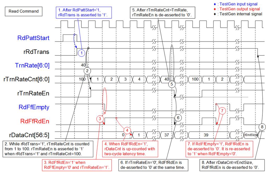
Figure 2‑7 Timing diagram of Read command in TestGen
1) The operation is started when RdPattStart is asserted to ‘1’. This signal is asserted only one clock cycle. After that, rRdTrans is asserted to ‘1’ to control rTrnRateEn It is de-asserted after all data is completely transferred.
2) While rRdTrans is asserted to ‘1’, rTrnRateCnt is up-counted from 1 to 100. The initial value of rTrnRateCnt is 100. rTrnRateEn is asserted to ‘1’ if rRdTrans=’1’ and rTrnRateCnt=100.
3) When rTrnRateEn is asserted to ‘1’ and FIFO has data (RdFfEmpty=’0’), RdFfRdEn is asserted to ‘1’ to read the test data from FIFO.
4) The data counter (rDataCnt) is up-counted after RdFfRdEn is asserted to ‘1’ for two clock cycles. It can be monitored to check the total amount of received data from FIFO.
5) This example sets TrnRate=40, so the maximum data rate is about 40/100 = 40% of maximum throughput of this logic. rTrnRateEn is asserted to ‘1’ for 40 cycles in every 100 cycles. After rTrnRateCnt=40, rTrnRateEn is de-asserted to ‘0’.
6) If rTrnRateEn is de-asserted to ‘0’, RdFfRdEn is de-asserted to ‘0’ to pause transmitting data at the same clock cycle.
7) If the FIFO is empty (RdFfEmpty=’1’), the read process is paused by de-asserting RdFfRdEn to ‘0’. The RdFfRdEn is re-asserted to ‘1’ when RdFfEmpty is de-asserted to ‘0’.
8) When total data count (rDataCnt) is equal to the total transfer size (rEndSize), rRdTrans is de-asserted to ‘0’ to complete the Read command.
2.2 NVMe
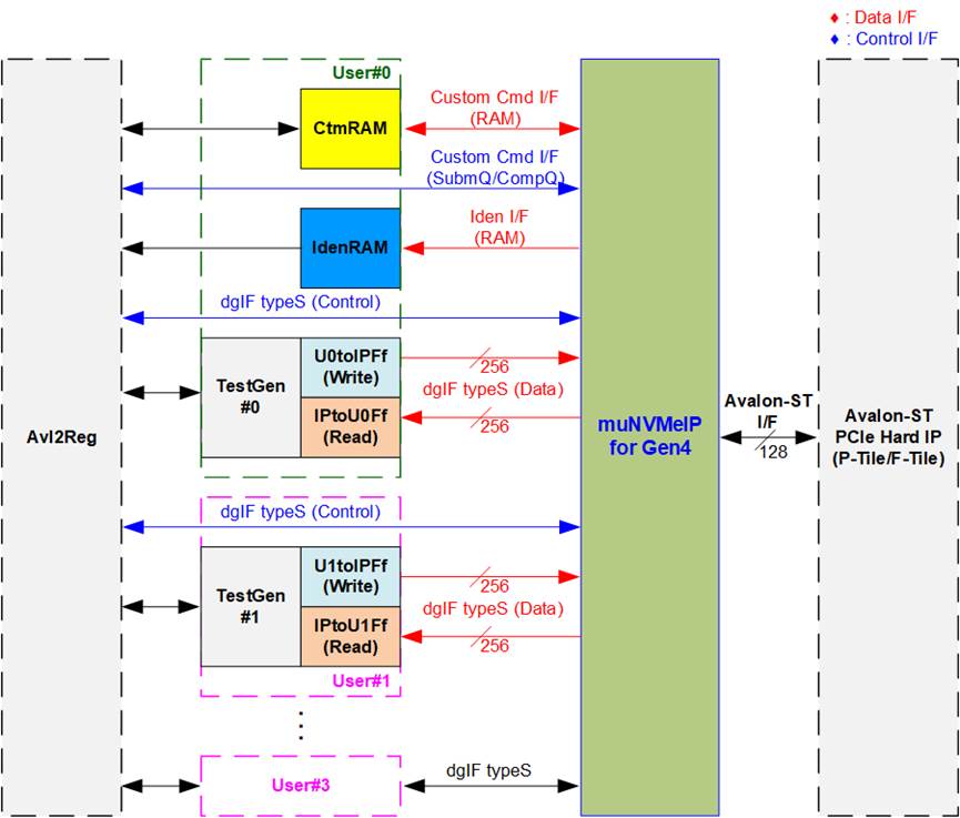
Figure 2‑8 NVMe hardware
Figure 2‑8 shows how to integrate muNVMe-IP for Gen4 in the system. Each user interface of muNVMe-IP consists of control interface and data interface. The control interface of User#0 supports to receive the command and the parameters via Custom command interface or dgIF typeS. Custom command interface is used when operating SMART command or Flush command. While the control interface of User#1 - #3 have only dgIF typeS to support Write command and Read command.
The data interface of User#0 has four interfaces, i.e., Custom command RAM interface, Identify interface, FIFO input interface (dgIF typeS), and FIFO output interface (dgIF typeS). While the data interface of User#1 - #3 have FIFO input interface and output interface (dgIF typeS). Data bus width of all data interface is 256 bits. The Custom command RAM interface is bi-directional interface while the other interfaces are uni-directional interface. In the reference design, the Custom command RAM interface is used for transferring data in receive direction only (storing SMART data transferred from muNVMe-IP to Avl2Reg).
2.2.1 muNVMe-IP for Gen4
The muNVMe-IP implements NVMe protocol of the host side to access one NVMe SSD directly without PCIe switch connection. The muNVMe-IP for Gen4 has four user interfaces for operating up to four commands at the same time. The first user (Main user) supports six commands, i.e., Write, Read, Identify, Shutdown, SMART, and Flush. The 2nd- the 4th user (Sub user) support two commands - Write and Read. The PCIe interface of muNVMe-IP can connect to the PCIe hard IP (P-Tile/F-Tile) directly. More details of muNVMe-IP are described in datasheet.
https://dgway.com/products/IP/NVMe-IP/dg_munvme_datasheet_g4_intel.pdf
2.2.2 PCIe Hard IP (P-Tile/F-Tile Avalon-ST Intel FPGA for PCIe)
This block is the hard IP in Intel FPGA device which implements Physical, Data Link, and Transaction Layers of PCIe protocol. More details are described in Intel FPGA document.
P-Tile Avalon-ST Intel FPGA for PCIe
https://www.intel.com/content/www/us/en/docs/programmable/683059/
F-Tile Avalon-ST Intel FPGA for PCIe
https://www.intel.com/content/www/us/en/docs/programmable/683140/
2.2.3 Two-port RAM
Two of two-Port RAMs, CtmRAM and IdenRAM, store data from Identify command and SMART command, respectively. IdenRAM is simple dual-port RAM which has one read port and one write port. The data size of Identify command is 8 Kbytes, so IdenRAM size is 8Kbyte. muNVMe-IP and Avl2Reg have different data bus size, 256-bit on muNVMe-IP but 32-bit on Avl2Reg. Therefore, IdenRAM has the different bus size on Write interface and Read interface. Besides, muNVMe-IP has double word enable to write only 32-bit data in some cases. The RAM setting on IP catalog of Quartus supports the write byte enable. Therefore, one bit of double word enable is extended to be 4-bit write byte enable as shown in Figure 2‑9.
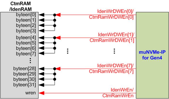
Figure 2‑9 Word enable to byte write enable connection
Bit[0], [1], …, [7] of WrDWEn are fed to bit[3:0], [7:4], …, [31:28] of IdenRAM byte write enable, respectively.
Comparing with IdenRAM, CtmRAM is implemented by Two-Port RAM (two read ports and two write ports) with byte write enable. The connection to convert from word enable of muNVMe-IP to byte enable of CtmRAM is similar to IdenRAM. Two-Port RAM is used to support the additional features when the customized custom command needs the data input. To support SMART command, using simple dual port RAM is enough. Though the data size returned from SMART command is 512 bytes, CtmRAM is implemented by 8Kbyte RAM for customized custom command.
2.3 CPU and Peripherals
32- bit Avalon-MM bus is applied to be the bus interface for CPU accessing the peripherals such as Timer and JTAG UART. The test system of muNVMe-IP is connected with CPU as a peripheral on 32-bit Avalon-MM bus. CPU assigns the different base address to access one peripheral for controlling and monitoring. Therefore, the test system must include the logic for connecting with Avalon-MM bus – Avl2Reg module.
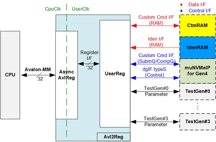
Figure 2‑10 CPU and peripherals hardware
Avl2Reg consists of AsyncAvlReg and UserReg. AsyncAvlReg is designed to convert the Avalon-MM signals to be the simple register interface which has 32-bit data bus size, similar to Avalon-MM data bus size. In addition, AsyncAvlReg includes asynchronous logic to support clock domain crossing between CpuClk domain and UserClk domain.
UserReg includes the register file for setting the parameters and storing the status signals of other modules in the test system, i.e., CtmRAM, IdenRAM, muNVMe-IP, and TestGen. More details of AsyncAvlReg and UserReg are described as follows.
2.3.1 AsyncAvlReg
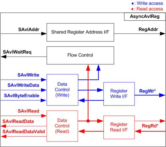
Figure 2‑11 AsyncAvlReg Interface
The signal on Avalon-MM bus interface can be split into three groups, i.e., Write channel (blue color), Read channel (red color), and Shared control channel (black color). More details of Avalon-MM interface specification are described in following document.
https://www.intel.com/content/dam/www/programmable/us/en/pdfs/literature/manual/mnl_avalon_spec.pdf
According to Avalon-MM specification, one command (write or read) can be operated at a time. The logics inside AsyncAvlReg are split into three groups, i.e., Write control logic, Read control logic, and Flow control logic. Flow control logic controls SAvlWaitReq to hold the next request from Avalon-MM interface if the current request does not finish. Write control and Write data I/F of Avalon-MM bus are latched and transferred to be Write register interface with clock domain crossing registers. Similarly, Read control I/F are latched and transferred to be Read register interface while the Read data is returned from Register Read I/F to Avalon-MM bus by using clock domain crossing registers. Address I/F of Avalon-MM is latched and transferred to Address register interface as well.
The simple register interface is compatible with single-port RAM interface for write transaction. The read transaction of the register interface is slightly modified from RAM interface by adding RdReq and RdValid signals for controlling read latency time. The address of register interface is shared for write and read transaction, so user cannot write and read the register at the same time. The timing diagram of the register interface is shown in Figure 2‑12.
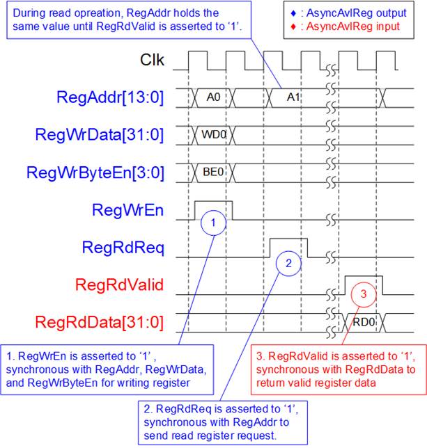
Figure 2‑12 Register interface timing diagram
1) To write register, the timing diagram is similar to single-port RAM interface. RegWrEn is asserted to ‘1’ with the valid signal of RegAddr (Register address in 32-bit unit), RegWrData (write data of the register), and RegWrByteEn (the write byte enable). Byte enable has four bits to be the byte data valid. Bit[0], [1], [2], and [3] are equal to ‘1’ when RegWrData[7:0], [15:8], [23:16], and [31:24] are valid, respectively.
2) To read register, AsyncAvlReg asserts RegRdReq to ’1’ with the valid value of RegAddr. 32-bit data is returned after receiving the read request. The slave must monitor RegRdReq to start the read transaction. In read operation, the address value (RegAddr) does not change until RegRdValid is asserted to ‘1’. Therefore, the address can be used for selecting the returned data by using multiple layers of multiplexer.
3) The read data is returned on RegRdData bus by the slave with asserting RegRdValid to ‘1’. After that, AsyncAvlReg forwards the read value to SAvlRead interface.
2.3.2 UserReg
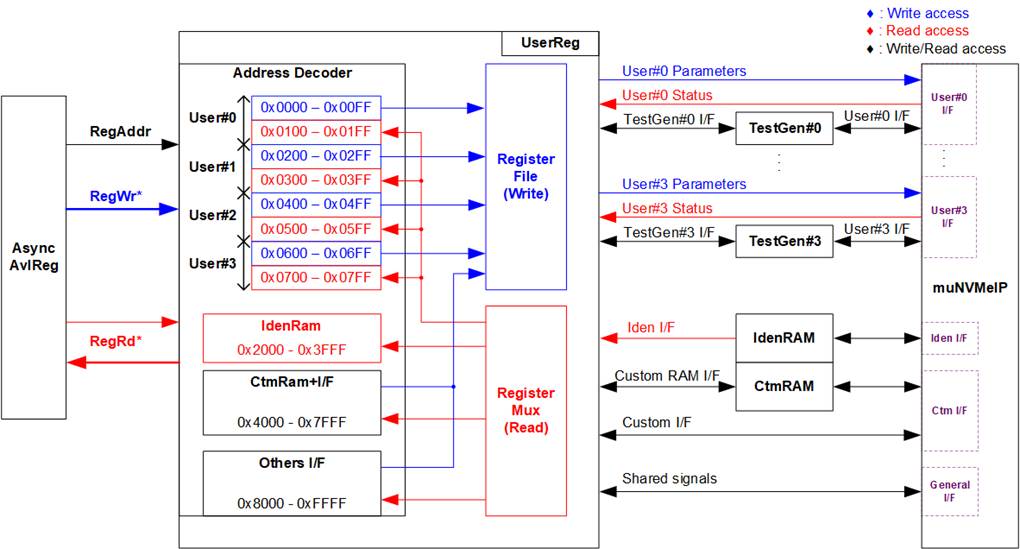
Figure 2‑13 UserReg Interface
The logic inside UserReg consists of Address decoder, RegFile, and RegMux. The address decoder decodes the address which is requested from AsyncAvlReg and then selects the active register for write or read transaction. The address range assigned in UserReg is split into eight areas, as shown in Figure 2‑13.
1) 0x0000 – 0x01FF: mapped to User#0 and TestGen#0
2) 0x0200 – 0x03FF: mapped to User#1 and TestGen#1
3) 0x0400 – 0x05FF: mapped to User#2 and TestGen#2
4) 0x0600 – 0x07FF: mapped to User#3 and TestGen#3
5) 0x2000 – 0x3FFF: mapped to read data from IdenRAM. This area is read-access only.
6) 0x4000 – 0x5FFF: mapped to write or read data with Custom command RAM interface. This area supports write-access and read-access but the demo shows only read access by running SMART command.
7) 0x6000 – 0x7FFF: mapped to Custom command interface
8) 0x8000 – 0xFFFF: mapped to other interfaces such as shared parameters for all Users, PCIe status, and IP version.
Address decoder decodes the upper bit of RegAddr for selecting the active hardware that is muNVMe-IP, TestGen#0-#3, IdenRAM, or CtmRAM. The register file inside UserReg is 32-bit bus size. Therefore, write byte enable (RegWrByteEn) is not applied in the test system and the CPU uses 32-bit pointer to access the hardware register.
To read register, multi-level multiplexers (mux) select the data to return to CPU, controlled by the address. The lower bit of RegAddr is fed to the submodule to select the active data. After that, the upper bit is applied in UserReg to select the data output of each submodule. Totally, the latency time of read data is equal to two clock cycles. Therefore, RegRdValid is created by RegRdReq with asserting two D Flip-flops. More details of the address mapping within UserReg module are shown in Table 2‑1.
Table 2‑1 Register map defintion
|
Address |
Register Name |
Description |
|
Rd/Wr |
(Label in the “munvmeiptest.c”) |
|
|
0x0000 – 0x01FF: Signal Interface of User#0 (muNVMe-IP) and TestGen#0 |
||
|
0x0000 – 0x00FF: Control signals of User#0 and TestGen#0 (Write access only) |
||
|
BA+0x0000 |
User#0 Address (Low) Reg |
[31:0]: Input to be bit[31:0] of User#0 start address as 512-byte unit (U0Addr[31:0] of muNVMe-IP) |
|
(U0ADRL_INTREG) |
||
|
BA+0x0004 |
User#0 Address (High) Reg |
[15:0]: Input to be bit[47:32] of User#0 start address as 512-byte unit (U0Addr[47:32] of muNVMe-IP) |
|
(U0ADRH_INTREG) |
||
|
BA+0x0008 |
User#0 Length (Low) Reg |
[31:0]: Input to be bit[31:0] of User#0 transfer length as 512-byte unit (U0Len[31:0] of muNVMe-IP) |
|
(U0LENL_INTREG) |
||
|
BA+0x000C |
User#0 Length (High) Reg |
[15:0]: Input to be bit[47:32] of User#0 transfer length as 512-byte unit (U0Len[47:32] of muNVMe-IP) |
|
(U0LENH_INTREG) |
||
|
BA+0x0010 |
User#0 Command Reg |
[2:0]: Input to be User#0 command (U0Cmd of muNVMe-IP) 000b: Identify, 001b: Shutdown, 010b: Write SSD, 011b: Read SSD, 100b: SMART, 110b: Flush, 101b/111b: Reserved When this register is written, the command request is sent to muNVMe-IP via User#0 I/F to start operating the command. |
|
(U0CMD_INTREG) |
||
|
BA+0x0014 |
User#0 Test Pattern Reg |
[2:0]: Select test pattern of TestGen#0 000b-Increment, 001b-Decrement, 010b-All 0, 011b-All 1, 100b-LFSR |
|
(U0PATTSEL_INTREG) |
||
|
BA+0x0018 |
User#0 Transfer Rate Reg |
[6:0]: Transfer Rate in percentage unit of TestGen#0. Valid from 1 – 100. For example, when this value=40, the maximum data rate is equal to 40% of 350 x 256-bit (11.2 GB/s) = 4480 MB/s. |
|
(U0TRNRATE_INTREG) |
||
|
0x0100 – 0x01FF: Status signals of User#0 and TestGen#0 (Read access only) |
||
|
BA+0x0100 |
User#0 Status Reg |
[0]: User#0 Busy of muNVMe-IP (‘0’: Idle, ‘1’: Busy) [1]: U0Error of muNVMe-IP (‘0’: Normal, ‘1’: Error) [2]: Data verification fail in TestGen#0 (‘0’: Normal, ‘1’: Error) |
|
(U0STS_INTREG) |
||
|
BA+0x0104 |
User#0 Error Type Reg |
[31:0]: Mapped to U0ErrorType[31:0] of muNVMe-IP to show error status |
|
(U0ERRTYPE_INTREG) |
||
|
BA+0x0108 |
User#0 Completion Status Reg |
[15:0]: Mapped to U0AdmCompStatus[15:0] of muNVMe-IP [31:16]: Mapped to U0IOCompStatus[15:0] of muNVMe-IP |
|
(U0COMPSTS_INTREG) |
||
|
BA+0x0110 |
User#0 Test pin (Low) Reg |
[31:0]: Mapped to U0TestPin[31:0] of muNVMe-IP |
|
(U0TESTPINL_INTREG) |
||
|
BA+0x0114 |
User#0 Test pin (High) Reg |
[15:0]: Mapped to U0TestPin[47:32] of muNVMe-IP |
|
(U0TESTPINH_INTREG) |
||
|
BA+0x0140- BA+0x015F |
User#0 Expected value Word0-7 Reg |
256-bit of the expected data at the 1st failure data in TestGen#0 when operating Read command 0x0140: Bit[31:0], 0x0144: Bit[63:32], …, 0x015C: Bit[255:224] |
|
(U0EXPPATW0-W7_INTREG) |
||
|
BA+0x0160- BA+0x017F |
User#0 Read value Word0-3 Reg |
256-bit of the read data at the 1st failure data in TestGen#0 when operating Read command 0x0160: Bit[31:0], 0x0164: Bit[63:32], …, 0x017C: Bit[255:224] |
|
(U0RDPATW0-W7_INTREG) |
||
|
BA+0x0180 |
User#0 Data Failure Address(Low) Reg |
[31:0]: Bit[31:0] of the byte address of the 1st failure data in TestGen#0 when operating Read command |
|
(U0RDFAILNOL_INTREG) |
||
|
BA+0x0184 |
User#0 Data Failure Address(High) Reg |
[24:0]: Bit[56:32] of the byte address of the 1st failure data in TestGen#0 when operating Read command |
|
(U0RDFAILNOH_INTREG) |
||
|
BA+0x0188 |
User#0 Current test byte (Low) Reg |
[31:0]: Bit[31:0] of the current test data size in TestGen#0 module |
|
(U0CURTESTSIZEL_INTREG) |
||
|
BA+0x018C |
User#0 Current test byte (High) Reg |
[24:0]: Bit[56:32] of the current test data size of TestGen#0 module |
|
(U0CURTESTSIZEH_INTREG) |
||
|
Address |
Register Name |
Description |
|
Rd/Wr |
(Label in the “munvmeiptest.c”) |
|
|
0x0200 – 0x07FF: Signal Interface of User#1-#3 (muNVMe-IP) and TestGen#1-#3 |
||
|
0x0200 – 0x02FF: Control signals of User#1 and TestGen#1 (Write access only) |
||
|
BA+0x0200- BA+0x021B |
Control signals of User#1/TestGen#1 |
Similar to 0x0000 – 0x001B which are the registers of User#0 and TestGen#0, these are mapped to User#1 and TestGen#1 instead. However, U1CMD_INTREG can be assigned by two values for two commands only – 010b: Write SSD and 011b: Read SSD. |
|
(U1ADRL_INTREG – U1TRNRATE_INTREG) |
||
|
0x0300 – 0x03FF: Status signals of User#1 and TestGen#1 (Read access only) |
||
|
BA+0x0300- BA+0x038F |
Status signals of User#1/TestGen#1 |
Similar to 0x0100 – 0x018F which are the registers of User#0 and TestGen#0, these are mapped to User#1 and TestGen#1 instead. However, there are some status signals that are available for User#0 only and not available for other Users, i.e., U0COMPSTS_INTREG[15:0], U0TESTPINL_INTREG[31:16], and U0TESTPINH_INTREG[15:0]. These registers are reserved for other Users. |
|
(U1STS_INTREG – U1CURTESTSIZEH_INTREG) |
||
|
0x0400 – 0x07FF: Signal interface of User#2-#3 and TestGen#2-#3 |
||
|
BA+0x0400- BA+0x078F |
(U2ADRL_INTREG – U3CURTESTSIZEH_INTREG) |
Similar to 0x0200 – 0x038F which are the registers of User#1 and TestGen#1, these are mapped to User#2-#3 and TestGen#2-#3. 0x400 – 0x58F: User#2 and TestGen#2 0x600 – 0x78F: User#3 and TestGen#3 |
|
0x2000 – 0x3FFF: IdenRAM (Read access only) |
||
|
BA+0x2000- BA+0x2FFF |
Identify Controller Data |
4Kbyte Identify Controller Data Structure |
|
(IDENCTRL_CHARREG) |
||
|
BA+0x3000-BA+0x3FFF |
Identify Namespace Data |
4Kbyte Identify Namespace Data Structure |
|
(IDENNAME_CHARREG) |
||
|
0x4000 – 0x5FFF: CtmRAM (Write/Read access) |
||
|
BA+0x4000-BA+0x5FFF |
Custom command Ram |
Connect to 8Kbyte CtmRAM interface for storing 512-byte data that is output from SMART Command. |
|
(CTMRAM_CHARREG) |
||
|
0x6000 – 0x7FFF: Custom Command Interface |
||
|
BA+0x6000- BA+0x603F |
Custom Submission Queue Reg |
[31:0]: Submission queue entry of SMART and Flush command. Input to be CtmSubmDW0-DW15 of muNVMe-IP. 0x6000: DW0, 0x6004: DW1, …, 0x603C: DW15 |
|
Wr |
(CTMSUBMQ_STRUCT) |
|
|
BA+0x6100-BA+0x610F |
Custom Completion Queue Reg |
[31:0]: CtmCompDW0-DW3 output from muNVMe-IP. 0x6100: DW0, 0x6104: DW1, …, 0x610C: DW3 |
|
Rd |
(CTMCOMPQ_STRUCT) |
|
|
Address |
Register Name |
Description |
|
Rd/Wr |
(Label in the “munvmeiptest.c”) |
|
|
0x8000 – 0xFFFF: Other Interfaces |
||
|
BA+0x8000 |
NVMe Timeout Reg |
[31:0]: Mapped to TimeOutSet[31:0] of muNVMe-IP |
|
Wr |
(NVMTIMEOUT_INTREG) |
|
|
BA+0x8100 |
PCIe Status Reg |
[0]: PCIe linkup status from PCIe hard IP (‘0’: No linkup, ’1’: linkup) [3:2]: Two lower bits to show PCIe link speed of PCIe hard IP. MSB is bit[16]. (000b: Not linkup, 001b: PCIe Gen1, 010b: PCIe Gen2, 011b: PCIe Gen3, 111b: PCIe Gen4) [6:4]: PCIe link width status from PCIe hard IP (001b: 1-lane, 010b: 2-lane, 100b: 4-lane) [13:8]: Current LTSSM State of PCIe hard IP. Please see more details of LTSSM value in Avalon-ST PCIe Hard IP datasheet [16]: The upper bit to show PCIe link speed of PCIe hard IP. Two lower bits are bit[3:2]. |
|
Rd |
(PCIESTS_INTREG) |
|
|
BA+0x8110 |
NVMe CAP Reg |
[31:0]: Mapped to NVMeCAPReg[31:0] of muNVMe-IP |
|
Rd |
(NVMCAP_INTREG) |
|
|
BA+0x8120 |
Total disk size (Low) Reg |
[31:0]: Mapped to LBASize[31:0] of muNVMe-IP
|
|
Rd |
(LBASIZEL_INTREG) |
|
|
BA+0x8124 |
Total disk size (High) Reg |
[15:0]: Mapped to LBASize[47:32] of muNVMe-IP [31]: Mapped to LBAMode of muNVMe-IP |
|
Rd |
(LBASIZEH_INTREG) |
|
|
BA+0x8200 |
IP Version Reg |
[31:0]: Mapped to IPVersion[31:0] of muNVMe-IP |
|
Rd |
(IPVERSION_INTREG) |
|
3 CPU Firmware
3.1 Test firmware (munvmeiptest.c)
After system boot-up, CPU runs following steps to finish the initialization process.
1) CPU initializes JTAG UART and Timer parameters.
2) CPU waits until PCIe connection links up (PCIESTS_INTREG[0]=‘1’).
3) CPU waits until muNVMe-IP completes initialization process (U0-U3STS_INTREG[0]=‘0’). If some errors are found, the process stops and the error message is displayed.
4) CPU displays PCIe link status (the number of PCIe lanes and the PCIe speed) by reading PCIESTS_INTREG[16:2].
5) CPU displays the main menu. There are five menus for running six commands of muNVMe-IP, i.e., Identify, Write, Read, SMART, Flush, and Shutdown.
More details of the sequence in each command that is designed in CPU firmware are described as follows.
3.1.1 Identify Command
This command can be requested by User#0 I/F. The sequence of the firmware when user selects Identify command is below.
1) Set U0CMD_INTREG=000b to send Identify command request on User#0 I/F of muNVMe-IP. After that, busy flag of User#0 I/F (U0STS_INTREG[0]) changes from ‘0’ to ‘1’.
2) CPU waits until the operation is completed or some errors are found by monitoring U0STS_INTREG[1:0].
Bit[0] is de-asserted to ‘0’ after finishing operating the command. Next, the data from Identify command of muNVMe-IP is stored in IdenRAM.
Bit[1] is asserted to ‘1’ when some errors are detected. The error message is displayed on the console to show the error details, decoded from U0ERRTYPE_INTREG[31:0]. Finally, the process is stopped.
3) After busy flag (U0STS_INTREG[0]) is de-asserted to ‘0’, CPU displays some information decoded from IdenRAM (IDENCTRL_CHARREG) such as SSD model name and the information from muNVMe-IP output such as SSD capacity and LBA unit size (LBASIZEH/L_INTREG).
3.1.2 Write/Read Command
Write and Read command can be requested by User#0-#3 I/F. The sequence of the firmware when user selects Write/Read command is below.
1) Receive 4-user parameters such as command (Write, Read, or Disable), start address, transfer length, test pattern, and transfer rate from the console. If some inputs are invalid, the operation is cancelled.
Note: If LBA unit size = 4 Kbyte, start address and transfer length must be aligned to 8.
2) Get all inputs and set to U0-U3ADRL/H_INTREG, U0-U3LENL/H_INTREG, U0-U3PATTSEL_INTREG, and U0-U3TRNRATE_INTREG.
3) Set U0-U3CMD_INTREG[2:0] = 010b for Write command or 011b for Read command and then the command request is asserted to the user who runs the Write command or Read command. After that, busy flag of the active user (U0-U3STS_INTREG[0]) changes from ‘0’ to ‘1’.
4) CPU waits until the operation is completed or some errors (except verification error) are found by monitoring U0-U3STS_INTREG[2:0].
Bit[0] is de-asserted to ‘0’ when command of User#0-#3 is completed.
Bit[1] is asserted when error is detected in User#0-#3. After that, error message is displayed on the console to show the error details. Finally, the process is hanged up.
Bit[2] is asserted when data verification is failed in User#0-#3. After that, the verification error message is displayed. However, CPU is still running until the operation is done or user inputs any key to cancel operation.
While the command is running, current transfer size of the active user read from U0-U3CURTESTSIZEL/H_INTREG is displayed every second.
5) After busy flag (U0-U3STS_INTREG[0]) is de-asserted to ‘0’, CPU displays the test result of the active user on the console, i.e., total time usage, total transfer size, and transfer speed.
3.1.3 SMART Command
This command can be requested by User#0 I/F. The sequence of the firmware when user selects SMART command is below.
1) Set 16-Dword of Submission queue entry (CTMSUBMQ_STRUCT) to be SMART command value.
2) Set U0CMD_INTREG[2:0]=100b to send SMART command request on User#0 I/F of muNVMe-IP. After that, busy flag of User#0 I/F (U0STS_INTREG[0]) changes from ‘0’ to ‘1’.
3) CPU waits until the operation is completed or some errors are found by monitoring U0STS_INTREG[1:0].
Bit[0] is de-asserted to ‘0’ after finishing operating the command. Next, the data from SMART command of muNVMe-IP is stored in CtmRAM.
Bit[1] is asserted when some errors are detected. The error message is displayed on the console to show the error details, decoded from U0ERRTYPE_INTREG[31:0]. Finally, the process is stopped.
4) After busy flag (U0STS_INTREG[0]) is de-asserted to ‘0’, CPU displays some information decoded from CtmRAM (CTMRAM_CHARREG), i.e., Remaining Life, Percentage Used, Temperature, Total Data Read, Total Data Written, Power On Cycles, Power On Hours, and Number of Unsafe Shutdown.
More details of SMART log are described in NVM Express Specification.
https://nvmexpress.org/resources/specifications/
3.1.4 Flush Command
This command can be requested by User#0 I/F. The sequence of the firmware when user selects Flush command is below.
1) Set 16-Dword of Submission queue entry (CTMSUBMQ_STRUCT) to be Flush command value.
2) Set U0CMD_INTREG[2:0]=110b to send Flush command request on User#0 I/F of muNVMe-IP. After that, busy flag of User#0 I/F (U0STS_INTREG[0]) changes from ‘0’ to ‘1’.
3) CPU waits until the operation is completed or some errors are found by monitoring U0STS_INTREG[1:0].
Bit[0] is de-asserted to ‘0’ after finishing operating the command. Next, CPU returns to the main menu.
Bit[1] is asserted when some errors are detected. The error message is displayed on the console to show the error details, decoded from U0ERRTYPE_INTREG[31:0]. Finally, the process is stopped.
3.1.5 Shutdown Command
This command can be requested by User#0 I/F. The sequence of the firmware when user selects Shutdown command is below.
1) Set U0CMD_INTREG[2:0]=001b to send Shutdown command request on User#0 I/F of muNVMe-IP. After that, busy flag of User#0 I/F (U0STS_INTREG[0]) changes from ‘0’ to ‘1’.
2) CPU waits until the operation is completed or some errors are found by monitoring U0STS_INTREG[1:0].
Bit[0] is de-asserted to ‘0’ after finishing operating the command. After that, the CPU goes to the next step.
Bit[1] is asserted when some errors are detected. The error message is displayed on the console to show the error details, decoded from U0ERRTYPE_INTREG[31:0]. Finally, the process is stopped.
3) After busy flag (U0STS_INTREG[0]) is de-asserted to ‘0’, the SSD and muNVMe-IP change to inactive status. The CPU cannot receive the new command from user. The user must power off the test system.
3.2 Function list in Test firmware
|
int exec_ctm(unsigned int user_cmd) |
|
|
Parameters |
user_cmd: 4-SMART command, 6-Flush command |
|
Return value |
0: No error, -1: Some errors are found in the muNVMe-IP |
|
Description |
Run SMART command following in topic 3.1.3 (SMART Command) or Flush command following topic 3.1.4 (Flush Command). |
|
unsigned long long get_cursize(unsigned int user) |
|
|
Parameters |
user: 0-3 for User#0-#3, respectively |
|
Return value |
Read value of U0-U3CURTESTSIZEH/L_INTREG |
|
Description |
Read U0-U3CURTESTSIZEH/L_INTREG and return read value as function result. |
|
int get_param(userin_struct* userin) |
|
|
Parameters |
userin: Five inputs from user, i.e., command, start address, total length in 512-byte unit, test pattern, and transfer rate |
|
Return value |
0: Valid input, -1: Invalid input |
|
Description |
Receive the input parameters from the user and verify the value. When the input is invalid, the function returns -1. Otherwise, all inputs are updated to userin parameter. |
|
void iden_dev(void) |
|
|
Parameters |
None |
|
Return value |
None |
|
Description |
Run Identify command, following in topic 3.1.1 (Identify Command). |
|
void print_space(unsigned long long size_input) |
|
|
Parameters |
size_input: test size for displaying on the console |
|
Return value |
None |
|
Description |
Calculate the number of digits and the number of spaces to display size_input with alignment on the console. |
|
int setctm_flush(void) |
|
|
Parameters |
None |
|
Return value |
0: No error, -1: Some errors are found in the muNVMe-IP |
|
Description |
Set Flush command to CTMSUBMQ_STRUCT and call exec_ctm function to operate Flush command. |
|
int setctm_smart(void) |
|
|
Parameters |
None |
|
Return value |
0: No error, -1: Some errors are found in the muNVMe -IP |
|
Description |
Set SMART command to CTMSUBMQ_STRUCT and call exec_ctm function to operate SMART command. Finally, decode and display SMART information on the console |
|
void show_error(unsigned int user) |
|
|
Parameters |
user: 0-3 for User#0-#3, respectively |
|
Return value |
None |
|
Description |
Read U0-U3ERRTYPE_INTREG (selected by user input), decode the error flag, and display error message following the error flag. Also, call show_pciestat function to check the debug signal in the hardware. |
|
void show_pciestat(void) |
|
|
Parameters |
None |
|
Return value |
None |
|
Description |
Read PCIESTS_INTREG until the read value from two read times is stable. After that, display the read value on the console. Also, debug signal is read from U0-U3TESTPINL/H_INTREG. |
|
void show_result(unsigned int user, unsigned int cmd, unsigned int timeuseh, unsigned int timeusel) |
|
|
Parameters |
user: 0-3 for User#0-#3, respectively cmd: 0-Write, 1-Read timeuseh, timeusel: 64-bit read value of timer |
|
Return value |
None |
|
Description |
Print user channel, command, and total size by calling get_cursize and show_size function. After that, calculate total time usage from timeuseh and timeusel and then display in usec, msec, or sec unit. Finally, transfer performance is calculated and displayed in MB/s unit. |
|
void show_size(unsigned long long size_input) |
|
|
Parameters |
size_input: transfer size to display on the console |
|
Return value |
None |
|
Description |
Calculate and display the input value in MByte, GByte, or TByte unit |
|
void show_smart_hex16byte(volatile unsigned char *char_ptr) |
|
|
Parameters |
*char_ptr: Pointer of 16-byte SMART data |
|
Return value |
None |
|
Description |
Display 16-byte SMART data as hexadecimal unit |
|
void show_smart_int8byte(volatile unsigned char *char_ptr) |
|
|
Parameters |
*char_ptr: Pointer of 8-byte SMART data |
|
Return value |
None |
|
Description |
When the input value is less than 4 billion (32-bit), display 8-byte SMART data as decimal unit. Otherwise, display overflow message. |
|
void show_smart_size8byte(volatile unsigned char *char_ptr) |
|
|
Parameters |
*char_ptr: Pointer of 8-byte SMART data |
|
Return value |
None |
|
Description |
Display 8-byte SMART data as GB or TB unit. When the input value is more than limit (500 PB), the overflow message is displayed instead. |
|
void show_vererr(unsigned int user) |
|
|
Parameters |
user: 0-3-User#0-#3, respectively |
|
Return value |
None |
|
Description |
Read U0-U3RDFAILNOL/H_INTREG (error byte address), U0-U3EXPPATW0-W3_INTREG (expected value), and U0-U3RDPATW0-W3_INTREG (read value) to display verification error details on the console. |
|
void shutdown_dev(void) |
|
|
Parameters |
None |
|
Return value |
None |
|
Description |
Run Shutdown command, following in topic 3.1.5 (Shutdown Command) |
|
int wrrd_dev(void) |
|
|
Parameters |
None |
|
Return value |
0: No error, -1: Receive invalid input |
|
Description |
Run Write command or Read command, following in topic 3.1.2 (Write/Read Command). It calls show_result function to calculate and display transfer performance in Write/Read command. |
4 Example Test Result
The test results when running demo system by 1-user and 4-user are shown in Figure 4‑1 and Figure 4‑2. Two figures are displayed by using two different test environments. Figure 4‑1 shows the result when using 2 TB Addlink S95 SSD, 32 GB transfer size per user, and all zero test pattern which can show the best performance. While Figure 4‑2 shows the result when using 800 GB Intel P5800X SSD, 32 GB transfer size per user, and LFSR test pattern which can show the good performance in any conditions.
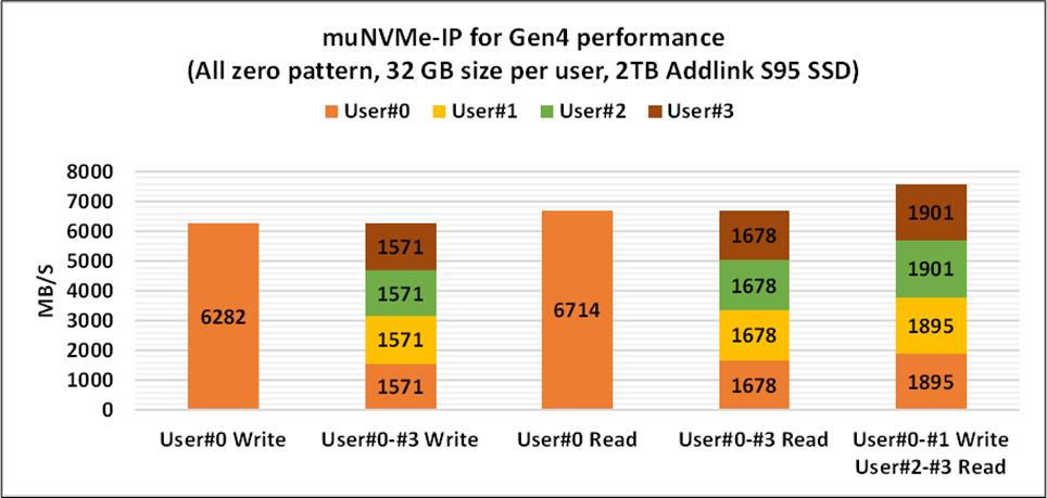
Figure 4‑1 Test Performance when using 2 TB Addlink S95 by 32 GB Zero pattern
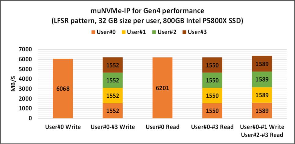
Figure 4‑2 Test Performance when using 800GB Intel P5800X by 32 GB LFSR pattern
As shown in Figure 4‑1 and Figure 4‑2, total performance of User#0 Write and User#0-#3 Write are equal. Similarly, total performance of User#0 Read and User#0-#3 Read are equal. The performance of each User when running User#0-#3 Write/Read operation (1571 MB/s or 1678 MB/s) is about the performance when running User#0 Write/Read (6282 MB/s or 6714 MB/s) divided by 4. Mixed Write-Read command (User#0-#1 Write, User#2-#3 Read) also shows the good load balancing for both test conditions. However, when the test condition is changed such as using larger transfer size and random test pattern, the performance of most SSDs will be reduced.
Typically, the SSD integrates the cache that can show the good performance for Write/Read command until the cache is full. Also, some SSDs implement the algorithm for processing data that can show the good performance when using all zero pattern, not random pattern. However, there are some SSDs such as 800 GB Intel P5800X that can show the good and stable performance when using LFSR pattern and large transfer size, as shown in Figure 4‑2.
5 Revision History
|
Revision |
Date |
Description |
|
1.1 |
23-Dec-22 |
Add maximum speed limitation feature |
|
1.0 |
4-Oct-22 |
Initial Release |
Copyright: 2022 Design Gateway Co,Ltd.