muNVMe-IP reference design manual
3.1 Test firmware (munvmeiptest.c)
3.2 Function list in Test firmware
1 Overview
The NVMe-IP provides a single user interface for sending one command at a time. The next command can be requested only after the completion of current one. Consequently, it is not possible for the user to simultaneously transmit both Write and Read commands to the SSD. However, the muNVMe-IP has been specifically designed to support this feature by offering two user interfaces for concurrent command transmission to the same SSD.
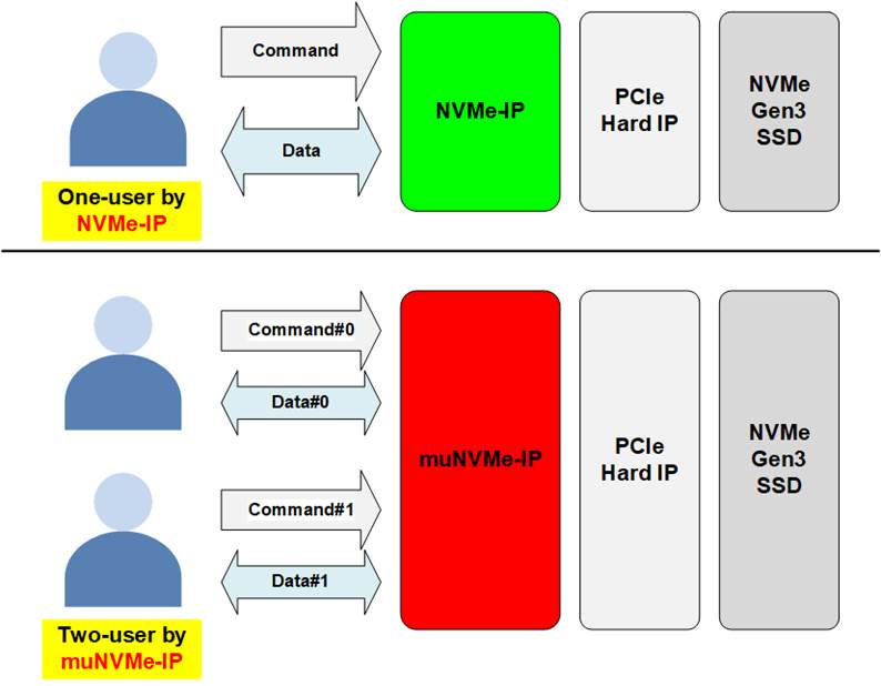
Figure 1‑1 NVMe-IP and muNVMe-IP comparison
Commands on these two user interfaces can be set by the same or values, allowing for combinations like Write-Write, Write-Read, and Read-Read commands. When executing the same command, the write or read performance for each user is about half value compared to using a single user interface. Meanwhile, the performance of mixed Write-Read commands depends on the characteristics of the SSD.
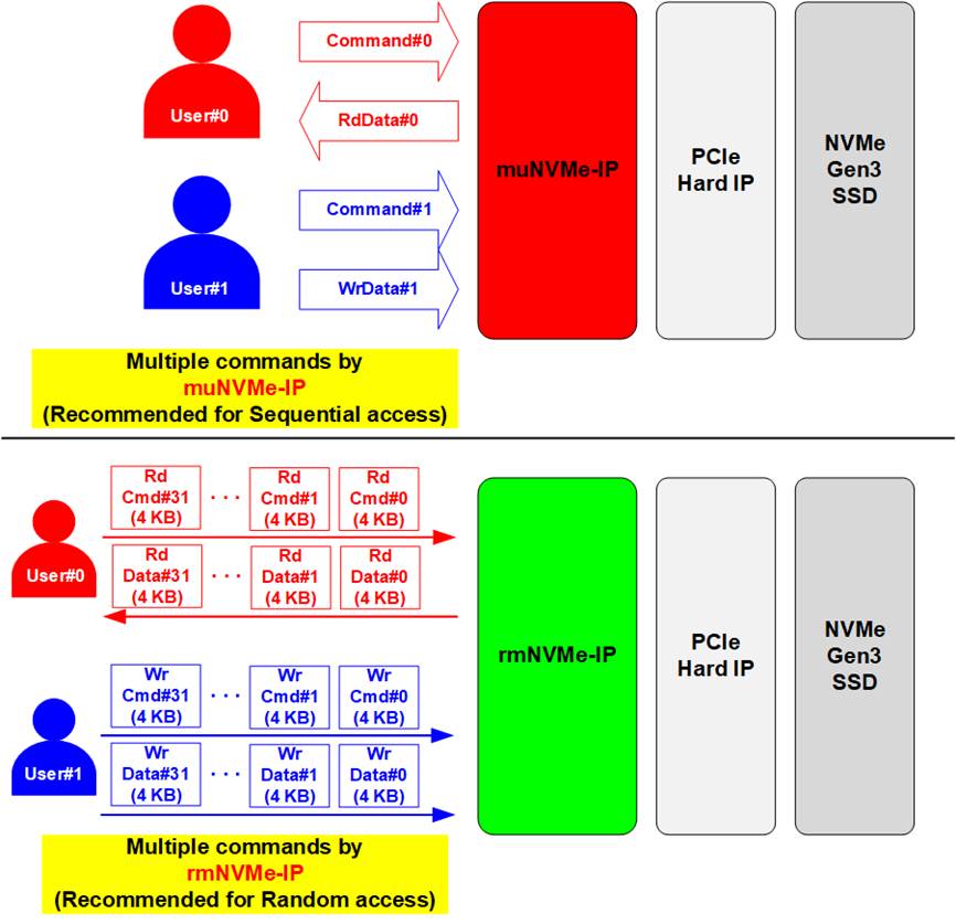
Figure 1‑2 muNVMe-IP and rmNVMe-IP comparison
Additionally, Design Gateway offers another NVMe-IP model known as rmNVMe-IP. The rmNVMe-IP features two user interfaces: User#0 for Read commands and User#1 for Write commands. To accommodate multiple commands with random access, each command has a fixed data size of 4 KB. In contrast, the muNVMe-IP permits a single command per user interface and allows up to two commands with selectable data sizes to be requested. Consequently, rmNVMe-IP is recommended for systems requiring random access, while muNVMe-IP is preferred option for systems necessitating high-performance data transfer with sequential access.
2 Hardware overview
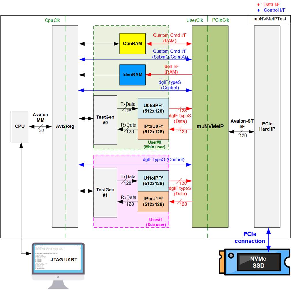
Figure 2‑1 muNVMe-IP demo hardware
The block diagram presented in Figure 2‑1 provides an overview of the submodules in the reference design. These submodules can be categorized into several functional groups.
1) Test Function: This group includes TestGen, which connects to the user interface of muNVMe-IP.
2) NVMe Function: Within this group, it includes CtmRAM, IdenRAM, U0-U1toIPFf, IPtoU0-U1Ff, muNVMe-IP, and PCIe Hard IP. These submodules handle NVMe and PCIe protocols.
3) CPU System: The CPU system includes the CPU and Avl2Reg, which facilitates communication between the CPU and the user. It is responsible for receiving test parameters from the user and displaying test results. In the final system, the CPU system can be replaced by a simple logic module designed to assign test parameters.
TestGen connects to the user interface of muNVMe-IP and is responsible for two main tasks. First is to generate a test data stream during Write command operation and store it at U0-U1toIPFf. Second is to verify the read data stream stored at IPtoU0-U1Ff during Read command operation. Each TestGen module is connected to a single user interface of muNVMe-IP, which means two TestGen modules are integrated and operate independently. Users have the flexibility to configure the maximum data transfer rate with each TestGen, helping to balance the data bandwidth between the two user interfaces.
The NVMe includes muNVMe-IP and PCIe hard IP for direct access to an NVMe SSD, without the need for a PCIe switch. CtmRAM and IdenRAM are used to store health data from SMART command and SSD information obtained from Identify command, respectively. Two FIFOs foreach user interface (U<i>toIFFf and IPtoU<i>Ff; i=0-1) illustrate the data interface of muNVMe-IP, simplifying control logic.
The CPU and Avl2Reg are designed for user interface via JTAG UART. User can set commands and the test parameters through the console, and the console provides real-time monitoring of the test hardware’s current status. The CPU firmware is implemented to provide an example sequence for executing commands on the two user interfaces.
In Figure 2‑1, three clock domains are displayed: CpuClk, UserClk, and PCIeClk.
1) CpuClk serves as the clock domain for the CPU system and its peripherals. It may be a stable clock that operates independently from other hardware.
2) UserClk is the user clock domain utilized for the operation of muNVMe-IP, RAM, FIFO, and TestGen. As specified in the muNVMe-IP datasheet, the clock frequency of UserClk must be equal to or greater than that of PCIeClk. In the reference design, UserClk is configured to operate at frequency of 275 MHz.
3) PCIeClk is the clock output generated by the PCIe hard IP, synchronized with the 128-bit Avalon-ST interface. The PCIeClk frequency is set to 250 MHz for 4-lane PCIe Gen3.
Further details regarding the hardware are provided below.
2.1 TestGen
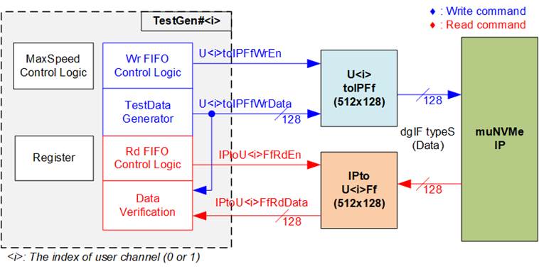
Figure 2‑2 TestGen interface
Each TestGen module is responsible for managing a single data interface of muNVMe-IP, facilitating data transfer for both Write and Read commands. During a Write command, TestGen transmits 128-bit test data to muNVMe-IP via U<i>toIPFf; where i=0-1. Conversely, for a Read command, TestGen receives test data from IPtoU<i>Ff, i=0-1. This received data is then compared to the expected value, ensuring data accuracy.
TestGen incorporates a ‘MaxSpeed Control’ to control the maximum speed of data transfer. This control logic manages the number of cycles in which data transfer is enabled for every 100 clock cycles during both write and read operations. The control logic activates the write or read enable signal of the FIFO when the FIFO is ready to write or read data, and the enable signal from the ‘MaxSpeed Control’ is asserted. If the user configures the enable cycles to the maximum value of 100, it results in optimal performance for writing or reading data with the SSD through muNVMe-IP.
The ‘Register’ within TestGen accepts user-defined test parameters, including the total transfer size, transfer direction, verification enable, and test pattern selector. The detailed hardware logic of TestGen is illustrated in Figure 2‑3.
Within Figure 2‑3, the user has the flexibility to configure four test parameters: Total transfer size (TrnLen), Start address (TrnAddr), Test pattern selector (PattSel), and Transfer rate (TrnRate) to specify the functionality of the TestGen module. This module serves three core functions. The first part illustrates the maximum speed control, the second part provides data flow control, and the final part details the generation of test data for use with the FIFO interface. TrnLen serves to calculate the end position of the operation (rEndSize), which is employed for comparison with the Data counter.
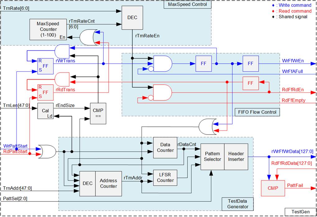
Figure 2‑3 TestGen hardware
In the upper block of Figure 2‑3, the ‘MaxSpeed Control’ includes a MaxSpeed Counter and a decoder. This component asserts the rTrnRateEn signal to 1b for a specified number of clock cycles within each 100-clock cycle interval. The duration of the rTrnRateEn signal assertion is determined by the TrnRate input signal. The MaxSpeed Counter operates during both write and read operations, as indicated by rWrTrans and rRdTrans being set to 1b. The enable signal, rTrnRateEn, serves to control the assertion of both WrFfWrEn and RdFfRdEn signals, which control data transfer during write and read operations.
In the central block of Figure 2‑3, we focus on data flow control. Two signals, WrFfAFull and RdFfEmpty, are integral to the FIFO interface for flow control. When the FIFO reaches its capacity (indicated by WrFfAFull=1b) or attains its maximum transfer rate (indicated by rTrnRateEn=0b), the WrFfWrEn signal is set to 0b, effectively pausing data transfer into the FIFO. During a read operation, when data is available within the FIFO (indicated by RdFfEmpty=0b) and data rate does not reach the limitation (indicated by rTrnRateEn=1b), the system retrieves this data for comparison by setting the RdFfRdEn to 1b. It is important to note that both write and read operations are completed when the total transferred data matches the user-defined value. Consequently, the counter logic is designed to track the amount of data transferred during this command, and upon command completion, both WrFfWrEn and RdFfRdEn must be de-asserted.
The lower block of Figure 2‑3 outlines the methods for generating test data, either for writing to the FIFO or for data verification. There are five available test patterns: all-zero, all-one, 32-bit incremental data, 32-bit decremental data, and LFSR. These patterns are selected by the Pattern Selector.
For the all-zero or all-one pattern, every bit of the data is set to zero or one, respectively. Conversely, the other test patterns are designed by separating the data into two parts to create unique test data within every 512-byte data, as shown in Figure 2‑4.
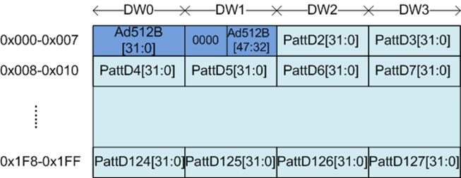
Figure 2‑4 Test pattern format in each 512-byte data for Increment/Decrement/LFSR pattern
Each 512-byte data block consists of a 64-bit header in Dword#0 and Dword#1, followed by the test data in the remaining words of the 512-byte data (Dword#2 – Dword#127). The header is created using the Address counter block, which operates in 512-byte units. The initial value of the Address counter is configured by the user and increases after transferring each 512-byte data.
The content of the remaining Dwords (DW#2 – DW#127) depend on the pattern selector, which could be 32-bit incremental data, 32-bit decremental data, or the LFSR pattern. The 32-bit incremental data is designed using the Data counter, while the decremental data can be created by connecting NOT logic to the incremental data. The LFSR pattern is generated using the LFSR counter, using the equation x^31 + x^21 + x + 1. To generate 128-bit test data, four 32-bit LFSR data are produced within a single clock cycle using look-ahead logic.
This Test data is used either as write data for the FIFO or for comparison with the data read from the FIFO. When data verification fails, the Fail flag is asserted to 1b.
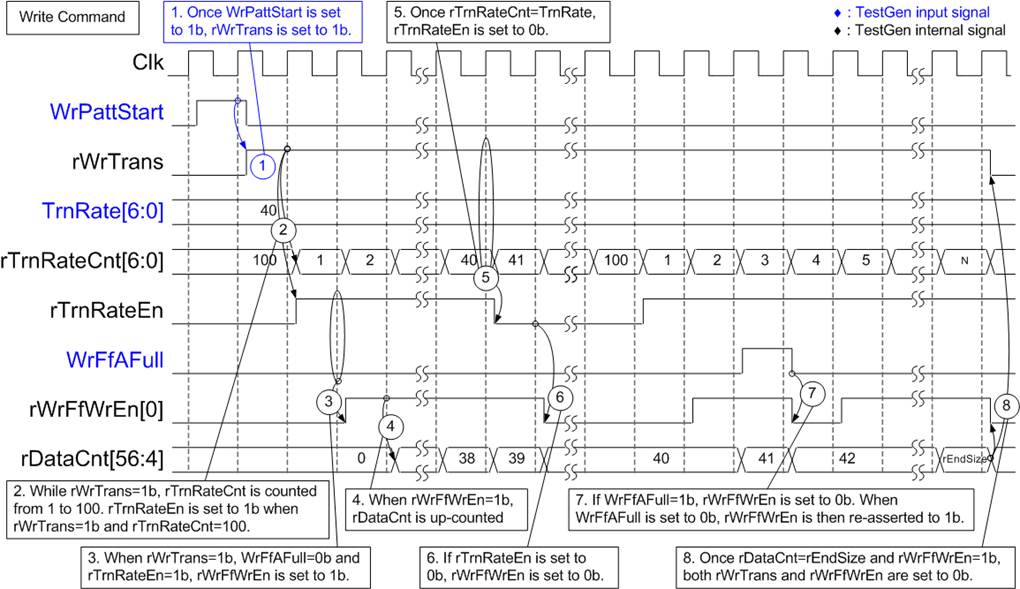
Figure 2‑5 Timing diagram of Write operation in TestGen
1) The operation starts when WrPattStart is asserted to 1b. This signal is asserted for a single clock cycle. Following this, rWrTrans is set to 1b to indicate that a Write operation is in progress. It is de-asserted upon the completion of the operation.
2) While rWrTrans is maintained at 1b, rTrnRateCnt increments from 1 to 100. The initial value of rTrnRateCnt is 100. rTrnRateEn is asserted to 1b if both rWrTrans=1b and rTrnRateCnt=100.
3) When both rWrTrans and rTrnRateEn are set to 1b and the FIFO is not full (WrFfAFull=0b), rWrFfWrEn is set to 1b for writing the test data to the FIFO.
4) The data counter (rDataCnt) increments when rWrFfWrEn is set to 1b. Therefore, it can be monitored to keep track of the total amount of data transmitted to the FIFO.
5) In this example, TrnRate is set to 40, resulting in a maximum data rate of approximately 40/100, or 40% of the maximum throughput of this logic. rTrnRateEn remains asserted at 1b for 40 cycles within every 100 cycles. After rTrnRateCnt=40, rTrnRateEn is de-asserted to 0b.
6) If rTrnRateEn is de-asserted to 0b, rWrFfWrEn is also de-asserted to 0b, pausing the data transmission.
7) When the FIFO is almost full (WrFfAFull=1b), the write process is paused by de-asserting rWrFfWrEn to 0b. rWrFfWrEn is re-asserted to 1b when WrFfAFull transitions from 1b to 0b.
8) Once the total data count (rDataCnt) equals the total transfer size (rEndSize), both rWrTrans and rWrFfWrEn are de-asserted to 0b, marking the completion of the Write command.
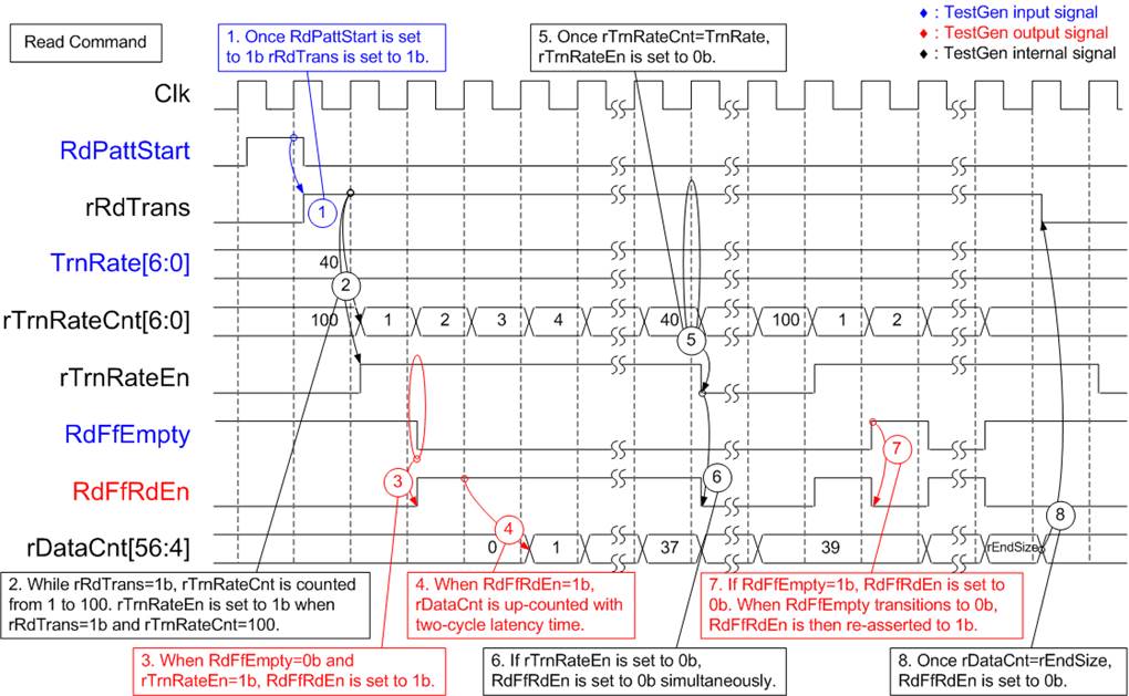
Figure 2‑6 Timing diagram of Read operation in TestGen
1) The operation starts when RdPattStart is asserted to 1b. This signal is asserted for a single clock cycle. Following this, rRdTrans is set to 1b to manage rTrnRateEn It is de-asserted after all data has been completely transferred.
2) While rRdTrans is maintained at 1b, rTrnRateCnt increments from 1 to 100. The initial value of rTrnRateCnt is 100. rTrnRateEn is asserted to 1b if both rRdTrans=1b and rTrnRateCnt=100.
3) When rTrnRateEn is asserted to 1b and the FIFO contains data (RdFfEmpty=0b), RdFfRdEn is set to 1b for reading data from the FIFO.
4) The data counter (rDataCnt) increments after RdFfRdEn is set to 1b for two clock cycles. This counter can be monitored to keep track of the total amount of data received from the FIFO.
5) In this example, TrnRate is set to 40, resulting in a maximum data rate of approximately 40/100, or 40% of the maximum throughput of this logic. rTrnRateEn remains asserted at 1b for 40 cycles within every 100 cycles. After rTrnRateCnt=40, rTrnRateEn is de-asserted to 0b.
6) If rTrnRateEn is de-asserted to 0b, RdFfRdEn is also de-asserted to 0b in the same clock cycle, effectively pausing data transmission.
7) When the FIFO is empty (RdFfEmpty=1b), the read process is paused by de-asserting RdFfRdEn to 0b. RdFfRdEn is re-asserted to 1b when RdFfEmpty transitions from 1b to 0b.
8) Once the total data count (rDataCnt) equals the total transfer size (rEndSize), rRdTrans is de-asserted to 0b, marking the completion of the Read command.
2.2 NVMe
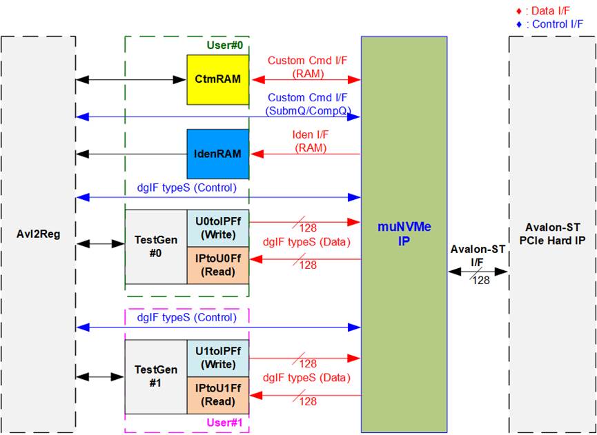
Figure 2‑7 NVMe hardware
In the reference design, each user interface of muNVMe-IP comprises both a control interface and a data interface. The User#0 control interface is responsible for receiving commands and parameters from either the Custom command interface or the dgIF typeS, depending on the type of command. Specifically, the Custom command interface is utilized when operating SMART or Flush command. While the User#1 control interface employs the dgIF typeS to execute Write and Read commands.
Besides, the User#0 data interface of muNVMe-IP uses four different interfaces, all with a data bus width of 128-bit. These interfaces include the Custom command RAM interface, Identify interface, FIFO input interface (dgIF typeS), and FIFO output interface (dgIF typeS). The Custom command RAM interface is a bi-directional interface, whereas the remaining interfaces are unidirectional interfaces. In the reference design, the Custom command RAM interface is used for one-way data transfer when muNVMe-IP transmits SMART data to Avl2Reg. For User#1 data interface, the FIFO input and output interfaces (dgIF typeS) are applied for executing Write and Read commands.
2.2.1 muNVMe-IP
The muNVMe-IP implements the NVMe protocol on the host side for enabling direct access to an NVMe SSD without PCIe switch connection. It offers two user interfaces, allowing users to send two command requests concurrently.
The first user, known as the Main user, can issue six commands, including Write, Read, Identify, Shutdown, SMART, and Flush. On the other hand, the second user, known as the Sub user, is capable of sending two specific commands: Write and Read.
The muNVMe-IP can be directly connected to the PCIe hard IP. More information on the muNVMe-IP is available in the detailed datasheet at the following link.
https://dgway.com/products/IP/NVMe-IP/dg_munvme_datasheet_intel/
2.2.2 Avalon-ST PCIe Hard IP
This block represents the hard IP integrated into Intel FPGAs, which is responsible for implementing the Physical, Data Link, and Transaction Layers of the PCIe specification. For more comprehensive information, please refer to the following documents.
ArriaV Avalon-ST Interface for PCIe Solutions User Guide
https://www.intel.com/content/dam/www/programmable/us/en/pdfs/literature/ug/ug_a5_pcie_avst.pdf
Stratix V Avalon-ST Interface for PCIe Solutions User Guide
https://www.intel.com/content/dam/www/programmable/us/en/pdfs/literature/ug/ug_s5_pcie_avst.pdf
Intel Arria10 and Intel Cyclone 10 GX Avalon-ST Interface for PCIe Solutions User Guide
https://www.intel.com/content/dam/www/programmable/us/en/pdfs/literature/ug/ug_a10_pcie_avst.pdf
2.2.3 Two-port RAM
Within this reference design, two 2-Port RAMs, CtmRAM and IdenRAM, store the returned data from Identify command and SMART command, respectively. Specifically, IdenRAM is designed with an 8 KB capacity, storing the 8 KB data response from the Identify command.
The data bus size for muNVMe-IP and Avl2Reg differ, with muNVMe-IP having a 128-bit size and Avl2Reg having a 32-bit size. As a result, IdenRAM is configured as an asymmetric RAM, with different bus sizes for its Write and Read interfaces.
muNVMe-IP is equipped with a double-word enable, enabling it to write only 32-bit data under certain cases. In the Quartus tool, the RAM settings support write byte enable functionality, and this double-word enable can be extended to a 4-bit write byte enable, as shown in Figure 2‑8.
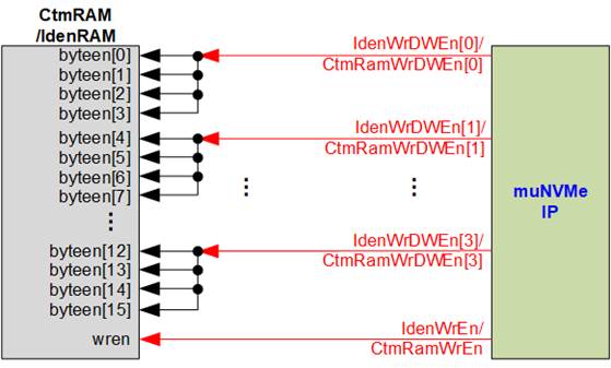
Figure 2‑8 Word enable to byte write enable connection
Each bit of WrDWEn is extended to be 4-bit of IdenWrEn, so bit[0], [1], [2], and [3] are then used to drive bit[3:0], [7:4], [11:8], and [15:12] of IdenWrEn, respectively.
On the other hand, CtmRAM is implemented as a 2-Port RAM with two read ports and two write ports, and with byte write enable. The connection from the double-word enable of muNVMe-IP to byte enable of CtmRAM is similar to that of IdenRAM. The 2-Port RAM is utilized to support additional features when the customized Custom command requires data input. For supporting SMART command, a simple dual-port RAM is sufficient, even though the data size returned from the SMART command is 512 bytes. However, CtmRAM is implemented with an 8KB RAM for the customized Custom command.
2.3 CPU and Peripherals
The CPU system uses a 32-bit Avalon-MM bus as the interface to access peripherals such as the Timer and JTAG UART. The system also integrates an additional peripheral to access the test logic by assigning a unique base address and address range. To support CPU read and write operations, the hardware logic must comply with the Avalon-MM bus standard. Avl2Reg module, as shown in Figure 2‑9, is designed to connect the CPU system via the Avalon-MM interface, in compliance with the standard.
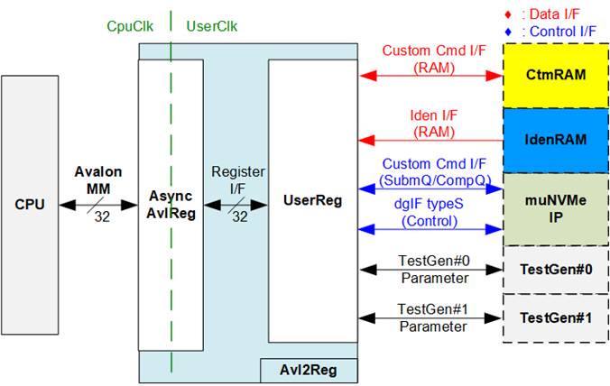
Figure 2‑9 CPU and peripherals hardware
Avl2Reg consists of AsyncAvlReg and UserReg. AsyncAvlReg converts Avalon-MM signals into a simple Register interface with a 32-bit data bus size, similar to the Avalon-MM data bus size. It also includes asynchronous logic to handle clock domain crossing between the CpuClk and UserClk domains.
UserReg includes the register file of the parameters and the status signals of other modules in the test system, including the CtmRAM, IdenRAM, muNVMe-IP, and TestGen. More details of AsyncAvlReg and UserReg are explained below.
2.3.1 AsyncAvlReg
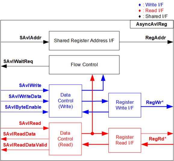
Figure 2‑10 AsyncAvlReg Interface
The Avalon-MM bus interface signal can be grouped into three categories: Write channel (blue), Read channel (red), and Shared control channel (black). More details about the Avalon-MM interface specification can be found in the following document.
https://www.intel.com/content/dam/www/programmable/us/en/pdfs/literature/manual/mnl_avalon_spec.pdf
According to Avalon-MM specification, a single command (write or read) can be executed at a time. AsyncAvlReg’s logic is divided into three groups: Write control logic, Read control logic, and Flow control logic. The flow control logic asserts SAvlWaitReq to hold the next request from the Avalon-MM interface if the current request has not finished. Write control and Write data I/F of the Avalon-MM bus are latched and transferred to the Write register interface with clock domain crossing registers. Similarly, Read control I/F are latched and transferred to be Read register interface. Afterward, the data returned from Register Read I/F is transferred to Avalon-MM bus with using clock domain crossing registers. The Address I/F of Avalon-MM is also latched and transferred to the Address register interface.
The Register interface is compatible with the single-port RAM interface for write transactions. However, the read transaction of the Register interface is slightly modified from RAM interface by adding RdReq and RdValid signals to control the read latency time. Since the address of the Register interface is shared for write and read transactions, the user cannot write and read the register at the same time. The timing diagram of the Register interface is shown in Figure 2‑11.
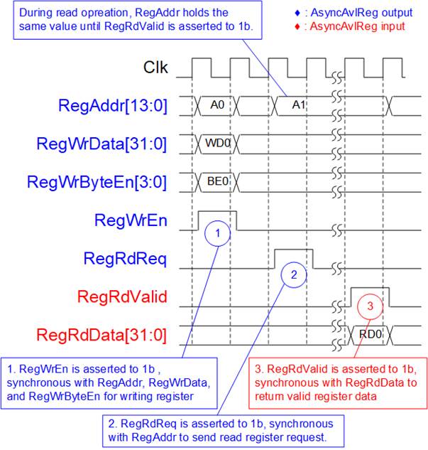
Figure 2‑11 Register interface timing diagram
1) Timing diagram to write register is similar to that of a single-port RAM. The RegWrEn signal is set to 1b, along with a valid RegAddr (Register address in 32-bit units), RegWrData (write data for the register), and RegWrByteEn (write byte enable). The byte enable consists of four bits that indicate the validity of the byte data. For example, bit[0], [1], [2], and [3] are set to 1b when RegWrData[7:0], [15:8], [23:16], and [31:24] are valid, respectively.
2) To read register, AsyncAvlReg sets the RegRdReq signal to 1b with a valid value for RegAddr. The 32-bit data is returned after the read request is received. The slave detects the RegRdReq signal being set to start the read transaction. In the read operation, the address value (RegAddr) remains unchanged until RegRdValid is set to 1b. The address can then be used to select the returned data using multiple layers of multiplexers.
3) The slave returns the read data on RegRdData bus by setting the RegRdValid signal to 1b. After that, AsyncAvlReg forwards the read value to the SAvlRead interface.
2.3.2 UserReg
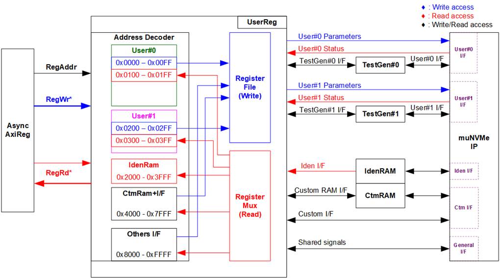
Figure 2‑12 UserReg Interface
The UserReg module comprises an Address decoder, a Register File, and a Register Mux. The Address decoder is responsible for decoding the address requested by AsyncAvlReg and selecting the active register for both write and read transactions. The assigned address range in UserReg is divided into six distinct areas, as illustrated in Figure 2‑12.
1) 0x0000 – 0x01FF: Mapped to User#0 of muNVMe-IP and TestGen#0.
2) 0x0200 – 0x03FF: Mapped to User#1 of muNVMe-IP and TestGen#1.
3) 0x2000 – 0x3FFF: Reserved for read access to IdenRAM. This area is read-access only.
4) 0x4000 – 0x5FFF: Mapped for write and read data via Custom command RAM interface. This area supports both write and read access. However, the demo shows only read access when executing the SMART command.
5) 0x6000 – 0x7FFF: Mapped to the Custom command interface.
6) 0x8000 – 0xFFFF: Mapped to other interfaces such as shared parameters for both User#0 and User#1 of muNVMe-IP, PCIe status, and IP version.
The Address decoder decodes the upper bits of RegAddr to select the active hardware (muNVMe-IP, TestGen#0-#1, IdenRAM, or CtmRAM). The Register File within UserReg features a 32-bit bus size, eliminating the need for write byte enable (RegWrByteEn) in the test system when the CPU utilizes a 32-bit pointer to set the hardware register.
To read registers, multi-level multiplexers (mux) are used to select the data to be returned to the CPU based on the address. The lower bits of RegAddr are directed to the submodule to select the active data from each submodule, while the upper bits in UserReg are used to select the returned data from each submodule. Consequently, the latency time for reading data equals two clock cycles. Therefore, RegRdValid is created by RegRdReq, with two D Flip-flops asserted. Further details of the address mapping within the UserReg module are shown in Table 2‑1.
Table 2‑1 Register map defintion
|
Address |
Register Name |
Description |
|
Rd/Wr |
(Label in the “munvmeiptest.c”) |
|
|
0x0000 – 0x01FF: Signal Interface of User#0 (muNVMe-IP) and TestGen#0 |
||
|
0x0000 – 0x00FF: Control signals of User#0 and TestGen#0 (Write access only) |
||
|
BA+0x0000 |
User#0 Address (Low) Reg |
[31:0]: Input to be bit[31:0] of User#0 start address as 512-byte unit (U0Addr[31:0] of muNVMe-IP) |
|
(U0ADRL_INTREG) |
||
|
BA+0x0004 |
User#0 Address (High) Reg |
[15:0]: Input to be bit[47:32] of User#0 start address as 512-byte unit (U0Addr[47:32] of muNVMe-IP) |
|
(U0ADRH_INTREG) |
||
|
BA+0x0008 |
User#0 Length (Low) Reg |
[31:0]: Input to be bit[31:0] of User#0 transfer length as 512-byte unit (U0Len[31:0] of muNVMe-IP) |
|
(U0LENL_INTREG) |
||
|
BA+0x000C |
User#0 Length (High) Reg |
[15:0]: Input to be bit[47:32] of User#0 transfer length as 512-byte unit (U0Len[47:32] of muNVMe-IP) |
|
(U0LENH_INTREG) |
||
|
BA+0x0010 |
User#0 Command Reg |
[2:0]: Input to be User#0 command (U0Cmd of muNVMe-IP) 000b: Identify, 001b: Shutdown, 010b: Write SSD, 011b: Read SSD, 100b: SMART, 110b: Flush, 101b/111b: Reserved When this register is written, the command request is sent to muNVMe-IP via User#0 I/F to start the command execution. |
|
(U0CMD_INTREG) |
||
|
BA+0x0014 |
User#0 Test Pattern Reg |
[2:0]: Select test pattern of TestGen#0 000b-Increment, 001b-Decrement, 010b-All 0, 011b-All 1, 100b-LFSR |
|
(U0PATTSEL_INTREG) |
||
|
BA+0x0018 |
User#0 Transfer Rate Reg |
[6:0]: Transfer Rate in percentage unit of TestGen#0. Valid from 1 – 100. For example, when this value=40, the maximum data rate equals to 40% of 275 x 128-bit (4400 MB/s), or 1760 MB/s. |
|
(U0TRNRATE_INTREG) |
||
|
0x0100 – 0x01FF: Status signals of User#0 and TestGen#0 (Read access only) |
||
|
BA+0x0100 |
User#0 Status Reg |
[0]: User#0 Busy of muNVMe-IP (0b: Idle, 1b: Busy) [1]: U0Error of muNVMe-IP (0b: Normal, 1b: Error) [2]: Data verification fail in TestGen#0 (0b: Normal, 1b: Error) |
|
(U0STS_INTREG) |
||
|
BA+0x0104 |
User#0 Error Type Reg |
[31:0]: Mapped to U0ErrorType[31:0] of muNVMe-IP to show error status |
|
(U0ERRTYPE_INTREG) |
||
|
BA+0x0108 |
User#0 Completion Status Reg |
[15:0]: Mapped to U0AdmCompStatus[15:0] of muNVMe-IP [31:16]: Mapped to U0IOCompStatus[15:0] of muNVMe-IP |
|
(U0COMPSTS_INTREG) |
||
|
BA+0x0110 |
User#0 Test pin (Low) Reg |
[31:0]: Mapped to U0TestPin[31:0] of muNVMe-IP |
|
(U0TESTPINL_INTREG) |
||
|
BA+0x0114 |
User#0 Test pin (High) Reg |
[15:0]: Mapped to U0TestPin[47:32] of muNVMe-IP |
|
(U0TESTPINH_INTREG) |
||
|
BA+0x0140- BA+0x014F |
User#0 Expected value Word0-3 Reg |
The 128-bit expected data of the 1st failure in TestGen#0 when executing a Read command. 0x0140: Bit[31:0], 0x0144: Bit[63:32], …, 0x014C: Bit[127:96] |
|
(U0EXPPATW0-W3_INTREG) |
||
|
BA+0x0160- BA+0x016F |
User#0 Read value Word0-3 Reg |
The 128-bit read data of the 1st failure in TestGen#0 when executing a Read command 0x0160: Bit[31:0], 0x0164: Bit[63:32], …, 0x016C: Bit[127:96] |
|
(U0RDPATW0-W3_INTREG) |
||
|
BA+0x0180 |
User#0 Data Failure Address(Low) Reg |
[31:0]: Bit[31:0] of the byte address of the 1st failure in TestGen#0 when executing a Read command |
|
(U0RDFAILNOL_INTREG) |
||
|
BA+0x0184 |
User#0 Data Failure Address(High) Reg |
[24:0]: Bit[56:32] of the byte address of the 1st failure in TestGen#0 when executing a Read command |
|
(U0RDFAILNOH_INTREG) |
||
|
BA+0x0188 |
User#0 Current test byte (Low) Reg |
[31:0]: Bit[31:0] of the current test data size in TestGen#0 module |
|
(U0CURTESTSIZEL_INTREG) |
||
|
BA+0x018C |
User#0 Current test byte (High) Reg |
[24:0]: Bit[56:32] of the current test data size in TestGen#0 module |
|
(U0CURTESTSIZEH_INTREG) |
||
|
Address |
Register Name |
Description |
|
Rd/Wr |
(Label in the “munvmeiptest.c”) |
|
|
0x0200 – 0x03FF: Signal Interface of User#1 (muNVMe-IP) and TestGen#1 |
||
|
0x0200 – 0x02FF: Control signals of User#1 and TestGen#1 (Write access only) |
||
|
BA+0x0200- BA+0x021B |
Control signals of User#1/TestGen#1 |
Similar to the registers in the range 0x0000 – 0x001B, which correspond to User#0 and TestGen#0, these registers are allocated for User#1 and TestGen#1. However, U1CMD_INTREG can only be assigned by two values: 010b for Write SSD and 011b for Read SSD commands. |
|
(U1ADRL_INTREG – U1TRNRATE_INTREG) |
||
|
0x0300 – 0x03FF: Status signals of User#1 and TestGen#1 (Read access only) |
||
|
BA+0x0300- BA+0x038F |
Status signals of User#1/TestGen#1 |
Similar to the registers in the range 0x0100 – 0x018F, which correspond to User#0 and TestGen#0, these registers are allocated for User#1 and TestGen#1. However, there are specific status signals available exclusively for User#0 and are not accessible to User#1. These signals include U0COMPSTS_INTREG[15:0], U0TESTPINL_INTREG[31:16], and U0TESTPINH_INTREG[15:0]. |
|
(U1STS_INTREG – U1CURTESTSIZEH_INTREG) |
||
|
0x2000 – 0x3FFF: IdenRAM (Read access only) |
||
|
BA+0x2000- BA+0x2FFF |
Identify Controller Data |
4KB Identify Controller Data Structure |
|
(IDENCTRL_CHARREG) |
||
|
BA+0x3000-BA+0x3FFF |
Identify Namespace Data |
4KB Identify Namespace Data Structure |
|
(IDENNAME_CHARREG) |
||
|
0x4000 – 0x5FFF: CtmRAM (Write/Read access) |
||
|
BA+0x4000-BA+0x5FFF |
Custom command Ram |
Connect to 8KB CtmRAM interface for storing 512-byte data output from SMART Command. |
|
(CTMRAM_CHARREG) |
||
|
0x6000 – 0x7FFF: Custom Command Interface |
||
|
BA+0x6000- BA+0x603F |
Custom Submission Queue Reg |
[31:0]: Submission queue entry of SMART and Flush command. Input to be CtmSubmDW0-DW15 of muNVMe-IP. 0x6000: DW0, 0x6004: DW1, …, 0x603C: DW15 |
|
Wr |
(CTMSUBMQ_STRUCT) |
|
|
BA+0x6100-BA+0x610F |
Custom Completion Queue Reg |
[31:0]: CtmCompDW0-DW3 output from muNVMe-IP. 0x6100: DW0, 0x6104: DW1, …, 0x610C: DW3 |
|
Rd |
(CTMCOMPQ_STRUCT) |
|
|
0x8000 – 0xFFFF: Other Interfaces |
||
|
BA+0x8000 |
NVMe Timeout Reg |
[31:0]: Mapped to TimeOutSet[31:0] of muNVMe-IP |
|
Wr |
(NVMTIMEOUT_INTREG) |
|
|
BA+0x8100 |
PCIe Status Reg |
[0]: PCIe linkup status from PCIe hard IP (0b: No linkup, 1b: linkup) [3:2]: PCIe link speed of PCIe hard IP. (00b: Not linkup, 01b: PCIe Gen1, 10b: PCIe Gen2, 11b: PCIe Gen3) [7:4]: PCIe link width status from PCIe hard IP (0001b: 1-lane, 0010b: 2-lane, 0100b: 4-lane, 1000b: 8-lane) [12:8]: Current LTSSM state of PCIe hard IP. Please see more details of LTSSM value in PCIe hard IP datasheet |
|
Rd |
(PCIESTS_INTREG) |
|
|
BA+0x8110 |
NVMe CAP Reg |
[31:0]: Mapped to NVMeCAPReg[31:0] of muNVMe-IP |
|
Rd |
(NVMCAP_INTREG) |
|
|
BA+0x8120 |
Total disk size (Low) Reg |
[31:0]: Mapped to LBASize[31:0] of muNVMe-IP
|
|
Rd |
(LBASIZEL_INTREG) |
|
|
BA+0x8124 |
Total disk size (High) Reg |
[15:0]: Mapped to LBASize[47:32] of muNVMe-IP [31]: Mapped to LBAMode of muNVMe-IP |
|
Rd |
(LBASIZEH_INTREG) |
|
|
BA+0x8200 |
IP Version Reg |
[31:0]: Mapped to IPVersion[31:0] of muNVMe-IP |
|
Rd |
(IPVERSION_INTREG) |
|
3 CPU Firmware
3.1 Test firmware (munvmeiptest.c)
Upon system boot-up, the CPU executes the following steps to complete the initialization process.
1) Initialize JTAG UART and Timer settings.
2) Wait for the PCIe connection to become active (PCIESTS_INTREG[0]=1b).
3) Wait until muNVMe-IP completes the initialization process (U0-U1STS_INTREG[0]=0b). If any errors occur during this phase, the process is halted, and error message is displayed.
4) Display the status of the PCIe link, which includes details such as the number of lanes and the speed. This information is obtained by reading the status in PCIESTS_INTREG[7:2].
5) Display the main menu, which offers five options to execute six commands of muNVMe-IP: Identify, Write, Read, SMART, Flush, and Shutdown.
Additional details of the sequence for each command in the CPU firmware are described in the following sections.
3.1.1 Identify Command
When user selects this option, the Identify command is requested to User#0. After that, the firmware follows this sequence.
1) Set U0CMD_INTREG[2:0]=000b to send the Identify command request to User#0 I/F. Subsequently, User#0 busy flag (U0STS_INTREG[0]) changes from 0b to 1b.
2) The CPU enters a waiting state, monitoring U0STS_INTREG[1:0] for the operation status or any error.
· Bit[0] is de-asserted to 0b when the command is completed. Also, the data response from Identify command, output from muNVMe-IP, is stored in IdenRAM.
· Bit[1] is asserted when an error is detected. In this case, the error message will be displayed on the console, revealing error details decoded from
U0ERRTYPE_INTREG[31:0]. The process will then be terminated.
3) Once User#0 busy flag (U0STS_INTREG[0]) is de-asserted to 0b, the CPU proceeds to display information that has been decoded from LBASIZEH/L_INTREG, which includes the SSD capacity and LBA unit size. Besides, further information, such as the SSD model, can be retrieved from the IdenRAM (IDENCTRL_CHARREG).
3.1.2 Write/Read Command
When the Write/Read command is selected, the firmware follows this sequence.
1) Receive commands for two users (Write, Read, or Disable), start address, transfer length, test pattern, and transfer rate from the console. If any of these inputs are invalid, the operation will be cancelled.
Note: If LBA unit size = 4 KB, the start address and transfer length must align to 8.
2) Once all the required inputs are obtained, set them to their respective registers:
U0-U1ADRL/H_INTREG, U0-U1LENL/H_INTREG, U0-U1PATTSEL_INTREG, and U0-U1TRNRATE_INTREG.
3) Iterate to set the command for each user when the Write or Read command is selected. Set U<i>CMD_INTREG[2:0] (where i=0 or 1) to 010b or 011b for Write or Read operation. Following this, the command request is asserted to User#<i> (where i=0 or 1), and the User#<i> busy flag (U<i>STS_INTREG[2:0]; where i=0 or 1) changes from 0b to 1b.
4) The CPU enters a waiting state, monitoring U0-U1STS_INTREG[2:0] for the operation status or any errors (excluding verification error).
· Bit[0] is de-asserted to 0b when the command is completed.
· Bit[1] is asserted when an error is detected. In this case, an error message will be displayed on the console, revealing error details decoded from U<i>ERRTYPE_INTREG[31:0] (where i=0 or 1). The process will then be terminated.
· Bit[2] is asserted when data verification fails. In this case, a verification error message will be displayed on the console, but the CPU will continue running until the operation is completed or until the user inputs any key to cancel the operation.
Additionally, during the command’s execution, the current transfer size, as read from
U0-U1CURTESTSIZEL/H_INTREG, will be displayed every second.
5) Once the busy flag (U0-U1STS_INTREG[0]) is de-asserted to 0b, the CPU proceeds to calculate and display the test results on the console. These results include the total time usage, the total transfer size, and the transfer speed.
3.1.3 SMART Command
When user selects this option, the SMART command is requested to User#0. After that, the firmware follows this sequence.
1) Configure the 16-Dword Submission Queue entry (CTMSUBMQ_STRUCT) with the SMART command value.
2) Set U0CMD_INTREG[2:0]=100b to send the SMART command request to User#0 I/F. This action causes User#0 busy flag (U0STS_INTREG[0]) to change from 0b to 1b.
3) The CPU enters a waiting state, monitoring U0STS_INTREG[1:0] for the operation status or any error.
· Bit[0] is de-asserted to 0b when the command is completed. Also, the data response from SMART command, output from muNVMe-IP, is stored in CtmRAM.
· Bit[1] is asserted when an error is detected. In this case, the error message will be displayed on the console, revealing error details decoded from
U0ERRTYPE_INTREG[31:0]. The process will then be terminated.
4) Once User#0 busy flag (U0STS_INTREG[0]) is de-asserted to 0b, the CPU proceeds to display information that has been decoded from CtmRAM (CTMRAM_CHARREG). This information includes Remaining Life, Percentage Used, Temperature, Total Data Read, Total Data Written, Power On Cycles, Power On Hours, and Number of Unsafe Shutdown.
For additional details regarding the SMART log, refer to the NVM Express Specification at
https://nvmexpress.org/specifications/
3.1.4 Flush Command
When user selects this option, the Flush command is requested to User#0. After that, the firmware follows this sequence.
1) Configure the 16-Dword Submission Queue entry (CTMSUBMQ_STRUCT) with the Flush command value.
2) Set U0CMD_INTREG[2:0]=110b to send the Flush command request to User#0 I/F. This action causes User#0 busy flag (U0STS_INTREG[0]) to change from 0b to 1b.
3) The CPU enters a waiting state, monitoring U0STS_INTREG[1:0] for the operation status or any error.
· Bit[0] is de-asserted to 0b when the command is completed.
· Bit[1] is asserted when an error is detected. In this case, the error message will be displayed on the console, revealing error details decoded from
U0ERRTYPE_INTREG[31:0]. The process will then be terminated.
4) Once User#0 busy flag (U0STS_INTREG[0]) is de-asserted to 0b, the CPU returns to the main menu.
3.1.5 Shutdown Command
When user selects this option, the Flush command is requested to User#0. After that, the firmware follows this sequence.
1) Set U0CMD_INTREG[2:0]=001b to send the Shutdown command request to User#0 I/F. This action causes User#0 busy flag (U0STS_INTREG[0]) to change from 0b to 1b.
2) The CPU enters a waiting state, monitoring U0STS_INTREG[1:0] for the operation status or any error.
· Bit[0] is de-asserted to 0b when the command is completed.
· Bit[1] is asserted when an error is detected. In this case, the error message will be displayed on the console, revealing error details decoded from
U0ERRTYPE_INTREG[31:0]. The process will then be terminated.
3) Once User#0 busy flag (U0STS_INTREG[0]) is de-asserted to 0b, both the SSD and muNVMe-IP become inactive, and the CPU will no longer accept new commands from the user. To resume testing, the user must power off and subsequently power on the system.
3.2 Function list in Test firmware
|
int exec_ctm(unsigned int user_cmd) |
|
|
Parameters |
user_cmd: 4-SMART command, 6-Flush command |
|
Return value |
0: No error, -1: Some errors are found in the muNVMe-IP |
|
Description |
Execute SMART command as outlined in section 3.1.3 (SMART Command) or execute Flush command as outlined in section 3.1.4 (Flush Command). |
|
unsigned long long get_cursize(unsigned int user) |
|
|
Parameters |
user: 0-User#0, 1-User#1 |
|
Return value |
Read value of U0-U1CURTESTSIZEH/L_INTREG |
|
Description |
The value of U0-U1CURTESTSIZEH/L_INTREG are read and converted to byte units before being return as the result of the function. |
|
int get_param(userin_struct* userin) |
|
|
Parameters |
userin: Five inputs from user, i.e., command, start address, total length in 512-byte unit, test pattern, and transfer rate |
|
Return value |
0: Valid input, -1: Invalid input |
|
Description |
Receive the input parameters from the user and verify the value. When the input is invalid, the function returns -1. Otherwise, all inputs are updated to userin parameter. |
|
void iden_dev(void) |
|
|
Parameters |
None |
|
Return value |
None |
|
Description |
Execute Identify command as outlined in section 3.1.1 (Identify Command). |
|
int setctm_flush(void) |
|
|
Parameters |
None |
|
Return value |
0: No error, -1: Some errors are found in the muNVMe-IP |
|
Description |
Set Flush command to CTMSUBMQ_STRUCT and call exec_ctm function to execute Flush command. |
|
int setctm_smart(void) |
|
|
Parameters |
None |
|
Return value |
0: No error, -1: Some errors are found in the muNVMe -IP |
|
Description |
Set SMART command to CTMSUBMQ_STRUCT and call exec_ctm function to execute SMART command. Finally, decode and display SMART information on the console |
|
void show_error(unsigned int user) |
|
|
Parameters |
user: 0-User#0, 1-User#1 |
|
Return value |
None |
|
Description |
Read U<i>ERRTYPE_INTREG (where ‘i’ is an index from user input), decode the error flag, and display error message corresponding to the detected error. Also, call ‘show_pciestat’ function to check the hardware’s debug signals. |
|
void show_pciestat(void) |
|
|
Parameters |
None |
|
Return value |
None |
|
Description |
Read PCIESTS_INTREG until the read value from two read times is stable. After that, display the read value on the console. Also, debug signal is read from U0-U1TESTPINL/H_INTREG. |
|
void show_result(unsigned int user, unsigned int cmd, unsigned int timeuseh, unsigned int timeusel) |
|
|
Parameters |
user: 0-User#0, 1-User#1 cmd: 2-Write, 3-Read timeuseh, timeusel: 64-bit read value of timer |
|
Return value |
None |
|
Description |
Print user channel, command, and total size by calling ‘get_cursize’ and ‘show_size’ functions. After that, calculate total time usage from global parameters (timeuseh and timeusel) and display in usec, msec, or sec unit. Finally, compute and display the transfer performance in MB/s unit. |
|
void show_size(unsigned long long size_input) |
|
|
Parameters |
size_input: transfer size to display on the console |
|
Return value |
None |
|
Description |
Calculate and display the input value in Mbyte or GByte unit. |
|
void show_smart_hex16byte(volatile unsigned char *char_ptr) |
|
|
Parameters |
*char_ptr: Pointer of 16-byte SMART data |
|
Return value |
None |
|
Description |
Display 16-byte SMART data as hexadecimal unit. |
|
void show_smart_int8byte(volatile unsigned char *char_ptr) |
|
|
Parameters |
*char_ptr: Pointer of 8-byte SMART data |
|
Return value |
None |
|
Description |
When the input value is less than 4 billion (32-bit), the 8-byte SMART data is displayed in decimal units. If the input value exceeds this limit, an overflow message is displayed. |
|
void show_smart_size8byte(volatile unsigned char *char_ptr) |
|
|
Parameters |
*char_ptr: Pointer of 8-byte SMART data |
|
Return value |
None |
|
Description |
Display 8-byte SMART data as GB or TB unit. When the input value is more than limit (500 PB), the overflow message is displayed instead. |
|
void show_vererr(unsigned int user) |
|
|
Parameters |
user: 0-User#0, 1-User#1 |
|
Return value |
None |
|
Description |
Read U<i>RDFAILNOL/H_INTREG (error byte address), U<i>EXPPATW0-W3_INTREG (expected value), and U<i>RDPATW0-W3_INTREG (read value) (where ‘i’ is an index from user input) to display verification error details on the console. |
|
void shutdown_dev(void) |
|
|
Parameters |
None |
|
Return value |
None |
|
Description |
Execute Shutdown command as outlined in section 3.1.5 (Shutdown Command) |
|
int wrrd_dev(void) |
|
|
Parameters |
None |
|
Return value |
0: No error, -1: Receive invalid input |
|
Description |
Execute Write/Read command as outlined in section 3.1.2 (Write/Read Command). In this function, ‘show_result’ is called to compute and display transfer performance in Write/Read command. |
4 Example Test Result
The performance results of executing Write and Read commands with 1-2 users on an 800 GB Intel P5800X SSD are illustrated in Figure 4‑1.
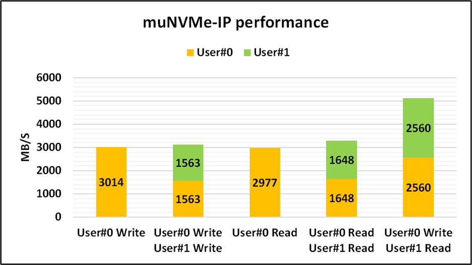
Figure 4‑1 Test Performance of muNVMe-IP demo
With specific SSDs, a good balance is observed when simultaneously executing Write and Read commands. The performance of both User#0 and User#1 is identical when executing the same command or the mixed Write-Read commands. When two users execute the same command, the overall performance closely matches that of a single user’s execution.
Nevertheless, it is important to note that with certain SSDs, there may be an imbalance in performance between User#0 and User#1 when executing mixed Write-Read commands, compared to executing the same command.
5 Revision History
|
Revision |
Date |
Description |
|
1.0 |
15-Nov-23 |
Initial Release |
Copyright: 2023 Design Gateway Co,Ltd.