2-Ch RAID0 NVMe-IP for Gen5 reference design manual
Rev1.0 7-Jul-23
2.2.2 PCIe Hard IP (R-Tile Avalon-ST Intel Hard IP for PCIe)
3.1 Test firmware (nvmeraid0g5test.c)
3.2 Function list in Test firmware
1 Introduction
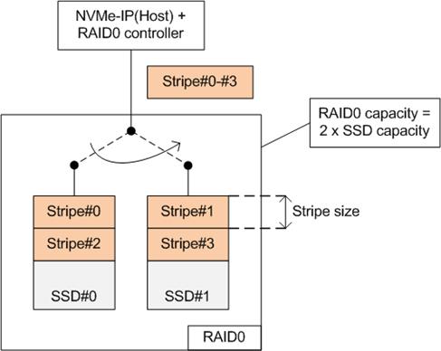
Figure 1‑1 RAID0 by 2 SSDs data format
The RAID0 system utilizes multiple storage device to expand total storage capacity and enhance write/read performance. Assuming the total number of devices connecting in the RAID0 system is represented by N, the overall storage capacity of RAID0 becomes N times the capacity of a single device. Similarly, the write and read performance of RAID0 is nearly N times that of a single device.
Figure 1‑1 illustrates the data format of RAID0. The data stream from the host side is divided into stripe unit for transferring data with each SSD at a time. The stripe size refers to the amount of data transferred with an SSD before switching to others. In this RAID0 reference design, the stripe size is set to 512 bytes.
For this demo, a system with two SSDs is employed. It is recommended to use the same SSD model for all channels to ensure compatibility and achieve optimal performance. As a result, the total capacity becomes twice that of a single SSD, while the write/read performance is nearly twice that of a single SSD.
In this demo, FIFO buffer implemented by Block Memory is utilized, which has smaller size compared to using DDR. Therefore, the buffer may not always be ready to transfer data when the SSD pauses data transmission for long time during the Write process. The performance tested in the demo represents the average speed, rather than the sustained rate. User have the flexibility to modify the RAID0 reference design by increasing the numbers of SSD to attain improved performance and larger capacity. Furthermore, user can integrate DDR as a data buffer in the system to support high-speed transfers at a sustained rate.
Before running the reference design, it is recommended to read NVMe-IP for Gen5 datasheet and the standard demo which is a single-channel demo, via the following links.
https://dgway.com/products/IP/NVMe-IP/dg_nvme_datasheet_g5_intel/
https://dgway.com/products/IP/NVMe-IP/dg_nvmeip_refdesign_g5_intel/
2 Hardware overview
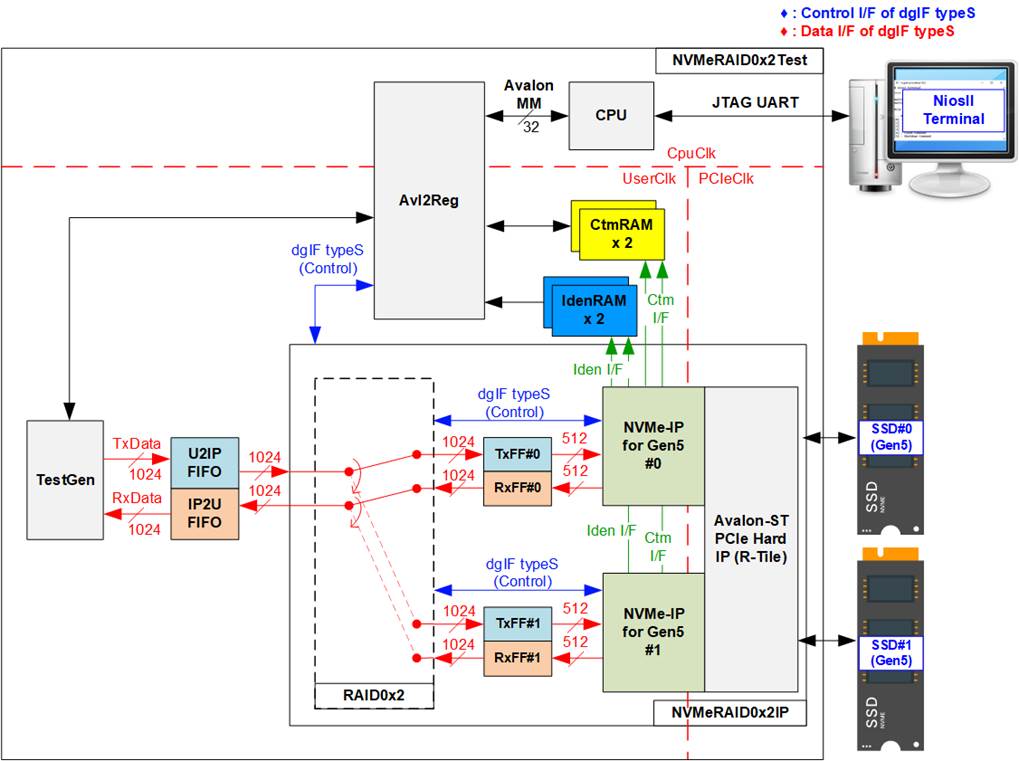
Figure 2‑1 2-Channel RAID0 NVMe-IP for Gen5 hardware overview
Thes test system consists of three hardware modules: TestGen, NVMeRAID0x2IP, and the CPU system consisting of CPU and Avl2Reg.
The TestGen module connects to the user interface of NVMeRAID0x2IP, which is specifically designed to be compatible with the NVMe-IP but doubling the data bus size. TestGen serves as an example of user logic for generating test data stream of Write command and verifying test data stream of Read command. The write and read data streams are stored at two FIFOs (U2IPFIFO and IP2UFIFO). TestGen always writes or reads data when the FIFO is ready, allowing for optimal transfer performance evaluation of the NVMeRAID0x2 system.
The NVMeRAID0x2IP module consists of RAID0x2, two NVMe-IPs, and a PCIe hard IP (R-Tile) enabling direct access to two NVMe Gen5 SSDs without PCIe switch. The PCIe hard IP is configured as 4x4-lane PCIe Gen5, capable of connecting up to 4 NVMe Gen5 SSDs. The CPU inputs command requests and parameters for each command though Avl2Reg module. RAID0x2 manages the command requests of two NVMe-IPs and controls the data transfer for Write and Read commands. The data interface of Custom and Identify commands is connected to RAMs, accessible by the CPU.
The CPU integrates a JTAG UART for communication with the user. The user can select the command type, configure command parameters, and monitor test progress through the console. The CPU firmware is designed to facilitate the execution of multiple test cases, ensuring comprehensive verification of IP functionality.
Figure 2‑1 illustrates three clock domains: CpuClk, UserClk, and PCIeClk. CpuClk is the clock domain for the CPU and its peripherals, requiring a stable clock. It can be independent clock from other hardware. UserClk is the main clock domain for the user logic (TestGen) and NVMeRAID0x2IP. According to the NVMe-IP for Gen5 datasheet, the frequency of UserClk must be equal to or greater than half of the PCIeClk frequency. In the reference design, UserClk frequency is set to 325 MHz. PCIeClk is generated by PCIe hard IP, synchronized with the 256-bit Avalon stream. The frequency of PCIeClk is 500 MHz for 4-lane PCIe Gen5. Using a lower frequency of PCIeClk is possible, but it will limit the maximum bandwidth on the user interface of PCIe hard IP to be lower than PCIe Gen5 performance. Further hardware details are described below.
2.1 TestGen
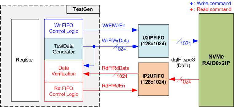
Figure 2‑2 TestGen interface
The TestGen module manages the data interface of NVMeRAID0x2IP, enabling data transfer for both Write and Read commands. In case of a Write command, TestGen sends 1024-bit test data to NVMeRAID0x2IP via U2IPFIFO. In contrast, for a Read command, the test data is received from IP2UFIFO for comparison with the expected value, ensuring data accuracy. Data bandwidth of TestGen is configured to match that of NVMeRAID0x2IP by operating at the same clock frequency and data bus size.
The control logic within TestGen guaranteees that the Write or Read enable signal is always asserted to 1b when the FIFO is ready to write or read data, respectively. This ensures that both U2IPFIFO and IP2UFIFO are always ready to transfer data with NVMeRAID0x2IP without delay, maximizing performance when writing and reading data with two SSDs through NVMeRAID0x2IP
To provide a flexible test environment, user can adjust test parameters via the console such as total transfer size, transfer direction, and test pattern selector. These test parameters are stored in the Register block. The detailed hardware logic of TestGen is illustrated in Figure 2‑3.
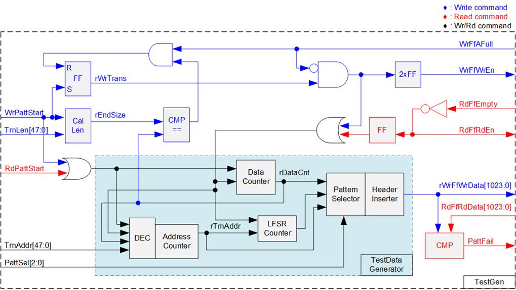
Figure 2‑3 TestGen hardware
Figure 2‑3 provides an overview of the TestGen module. The right side of the figure shows the utilization of flow control signals of FIFO, WrFfAFull and RdFfEmpty. During a write operation, if the FIFO becomes almost full (WrFfAFull=1b), WrFfWrEn is de-asserted to 0b to pause data transmission to the FIFO. Similarly, during a read operation, if there is data available in the FIFO (RdFfEmpty=0b), the logic reads data from the FIFO for comparison by asserting RdFfRdEn to 1b.
The left side of Figure 2‑3 shows the logic designed to count transfer size. Once the total data count (rDataCnt) matches the end size (rEndSize) set by the user, the write enable or read enable of the FIFO is de-asserted to 0b to halt data trasnfer. The lower side of Figure 2‑3 provides the details to generate test data for writing to the FIFO or verifying data from the FIFO. Five test patterns are available: all-zero, all-one, 32-bit incremental data, 32-bit decremental data, and LFSR, selected by Pattern Selector. Fpr all-zero or all-one pattern, each bit of data is fixed at zero or one, respectively. The remaining patterns involve splitting the data into two parts to create unique test data within each 512-byte data block, as shown in Figure 2‑4.
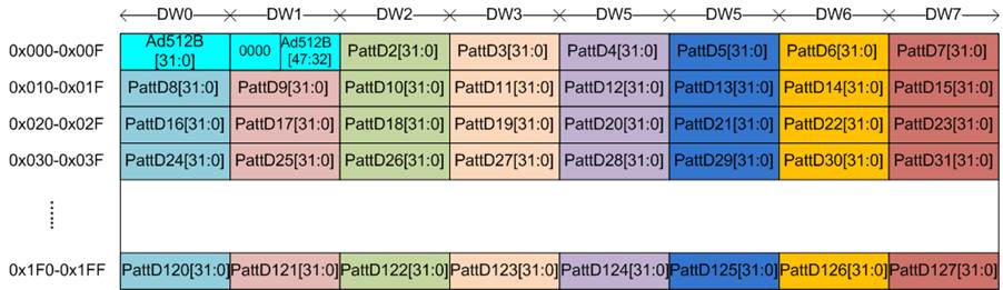
Figure 2‑4 Test pattern format in each 512-byte data for Increment/Decrement/LFSR pattern
The first two double words (Dword#0 and Dword#1) within each 512-byte block form a 64-bit header. The remaining words (Dword#2 � Dword#127) contain the actual test data. The header is created using the address counter block, operated in 512-byte unit (rTrnAddr). The initial value of the address counter is set by the user (TrnAddr), and incremented after finishing each 512-byte data transfer. The value of the remaining Dwords (DW#2 � DW#127) depends on the pattern selector, which may be 32-bit incremental data, 32-bit decremental data, or LFSR. The 32-bit incremental data is generated using Data counter, while the decremental data can be obtrained by connecting NOT logic to incremental data. The LFSR pattern is generated using the LFSR counter with the polynomial equation x^31 + x^21 + x + 1.
To generate 1024-bit test data using the LFSR pattern, the data is divided into eight sets of 128-bit data. Each set uses a different start value, as shown in Figure 2‑5.
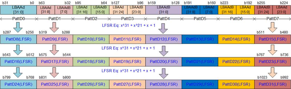
Figure 2‑5 1024-bit LFSR Pattern in TestGen
Using a look-ahead technique, four 32-bit LFSR data or 128-bit data can be generated per clock cycle, as represented by the same color in Figure 2‑5. The start value of each data set is derived from a 32-bit Logical LBA Address (LBAAd), with the application of the NOT logic to a specific bit of the LBAAd (LBAAdB) to create a unique start value for each 128-bit data set. The generated test data can then be written to the FIFO as write data or compared with the read data from the FIFO for verification. If the data verification process fails, the fail flag is set to 1b. The timing diagram for writing data to the FIFO is shown below.
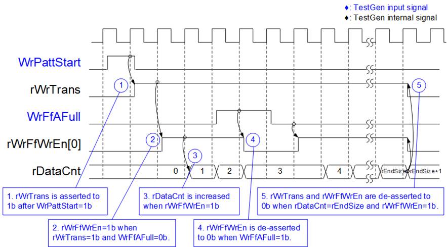
Figure 2‑6 Timing diagram of Write operation in TestGen
1) The write operation is initiated by setting WrPattStart signal to 1b for one clock cycle, which is followed by the assertion of rWrTrans to enable the control logic for generating write enable to FIFO.
2) If two conditions are met (rWrTrans is asserted to 1b during the write operation and the FIFO is not full, indicated by WrFfAFull=0b), the write enable (rWrFfWrEn) to FIFO is asserted to 1b.
3) The write enable is fed back to the counter to count the total amount of data in the write operation.
4) If FIFO is almost full (WrFfAFull=1b), the write process is paused by de-asserting rWrFfWrEn to 0b.
5) The write operation is finished when the total data count (rDataCnt) is equal to the set value (rEndSize). At this point, both rWrTrans and rWrFfWrEn are de-asserted to 0b.
Unlike the write enable, the read enable signal is not stopped by total data count and not started by start flag. For read transfer, the read enable of FIFO is controlled by the empty flag of FIFO. When the read enable is asserted to 1b, the data counter and the address counter are increased for counting the total amount of data and generating the header of expect value, respectively.
2.2 NVMeRAID0x2IP
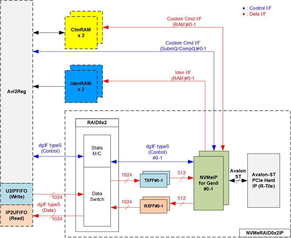
Figure 2‑7 NVMeRAID0x2IP hardware
In the reference design, the NVMeRAID0x2IP�s user interface consists of a control interface and a data interface. The control interface receives commands and parameters from either the Custom command interface or dgIF typeS, depending on the type of command. For instance, Custom command interface is used when operating SMART command, Flush command, or Secure Erase command.
On the other hand, the data interface of NVMeRAID0x2IP has four different interfaces, including Custom command RAM interface, Identify interface, FIFO input interface (dgIF typeS), and FIFO output interface (dgIF typeS). While the Custom command RAM interface is a bi-directional interface, the other interfaces are one directional interface. In the reference design, the Custom command RAM interface is used for one-directional data transfer when NVMeRAID0x2IP sends SMART data to Avl2Reg.
2.2.1 NVMe-IP for Gen5
The NVMe-IP implements NVMe protocol of the host side to direct access an NVMe SSD without PCIe switch connection. It supports seven commands, i.e., Write, Read, Identify, Shutdown, SMART, Flush, and Secure Erase. The NVMe-IP can connect to the PCIe Hard IP (R-Tile) directly. More details of NVMe-IP are described in datasheet.
https://dgway.com/products/IP/NVMe-IP/dg_nvme_datasheet_g5_intel/
2.2.2 PCIe Hard IP (R-Tile Avalon-ST Intel Hard IP for PCIe)
This block is hard IP in Intel FPGA device which implements Physical, Data Link, and Transaction Layers of PCIe protocol. More details are described in Intel FPGA document.
R-Tile Avalon-ST Intel FPGA for PCIe
https://www.intel.com/content/www/us/en/docs/programmable/683501/
2.2.3 Two-port RAM
Two of two-Port RAMs, CtmRAM and IdenRAM, store the returned data from Identify and SMART commands, respectively. IdenRAM is simple dual-port RAM with one read port and one write port and has a data size 8 Kbytes to store the 8 Kbyte data output from the Identify command. The data bus size for NVMe-IP and Avl2Reg differ, with NVMe-IP having a 512-bit size and Avl2Reg having a 32-bit size. As a result, IdenRAM is an asymmetric RAM with different bus sizes for its Write and Read interfaces. NVMe-IP also has a double-word enable, which allows it to write only 32-bit data in certain cases. The RAM setting on the IP catalog of Quartus enables write byte enable, so each bit of the double word enable is extended to a 4-bit write byte enable, as shown in Figure 2‑8.
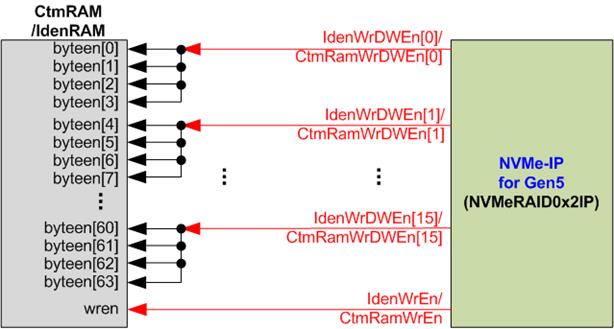
Figure 2‑8 Byte enable conversion logic
The 16 bits of the WrDWEn are used to drive the byte write enable of IdenRAM as follows: bits[0], [1], �, [15] of WrDWEn are fed to bits[3:0], [7:4], �, [63:60] of IdenRAM byte write enable.
On the other hand, CtmRAM is implemented as a two-Port RAM with two read ports and two write ports, and with byte write enable. The connection from the double-word enable of NVMe-IP to byte enable of CtmRAM is similar to that of IdenRAM. The two-Port RAM is utilized to support additional features when the customized Custom command requires data input. For supporting SMART command, a simple dual-port RAM is sufficient, even though the data size returned from the SMART command is 512 bytes. However, CtmRAM is implemented with an 8Kbyte RAM for the customized Custom command.
2.2.4 FIFO
Within NVMeRAID0x2IP, the data interface of each NVMe-IP is connected to two FIFOs: TxFF and RxFF. These FIFOs are applied for two purposes: buffering the data and converting the data bus size between the RAID0x2 interface, which has a size of 1024 bits, and the NVMe-IP interface, which has a size of 512 bits. Both TxFF and RxFF are asymmetric FIFOs with a capacity of 16 Kbytes.
2.2.5 RAID0x2
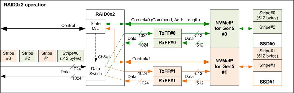
Figure 2‑9 RAID0x2 operation
RAID0x2 includes a state machine responsible for managing the control interface and a data switch for managing the data interface. When a new command request is received from Avl2Reg, the state machine decodes the command type and determines the corresponding parameters of each NVMe-IP. For instance, when executing the Write and Read commands, the state machine determines the address and transfer length required of each NVMe-IP. Then, the state machine generates a command request to the NVMe-IP.
Figure 2‑9 shows a detailed overview of the data flow to operate RAID0x2 function. The input data stream from the user (TestGen) is divided into a stripe size (512-byte units). RAID0 determines the first active NVMe-IP and transfers the first 512-byte data to it. In the example as shown in Figure 2‑9, a Write command is executed and the first active NVMe-IP is Ch#0. Consequently, Stripe#0 is stored in SSD#0 through TxFF#0 and NVMe-IP#0. Then, the active channel is switched to Ch#1. The next stripe (Stripe#1) is stored in SSD#1 through TxFF#1 and NVMe-IP#1. This process continues, with the active channel being toggled every 512-byte data transfer until all data has been transferred.
To determine the first active channel, it is based on the LSB of the start address in 512-byte units. When the LSB is 0b, the first active channel is Ch#0. Conversely, if the LSB is 1b, the first active channel becomes Ch#1.
The data switch uses multiple pipeline registers, resulting in overhead time for switching the active channel during the transfer of each 512-byte data. In the reference design, this overhead time amounts to 1 clock cycle of every 4 clock cycles (4 clock cycles is the time usage for 512-byte data transfer), equivalent to 25% of the overall operation time. To compensate for this overhead, the clock frequency of RAID0x2 must be set 25% higher than the NVMe based clock, corresponding to 312.5 MHz for PCIe Gen5 (125% of 250 MHz). In the reference design, 325 MHz is implemented for optimizing the Write/Read performance.
The user interface of RAID0x2 is designed to be compatible with the user interface of NVMe-IP, utilizing dgIF typeS. Table 2‑1 shows the detailed information of the user interface.
Table 2‑1 Signal description of RAID0x2 (only User interface)
|
Signal |
Dir |
Description |
|
Control I/F of dgIF typeS |
||
|
RstB |
In |
Synchronous reset signal. Active low. De-asserted to 1b when the Clk signal is stable |
|
Clk |
In |
User clock source to both RAID0x2 and NVMe-IP. The frequency of this clock must be equal to or greater than 325 MHz for PCIe Gen5 clock frequency of 250 MHz. |
|
UserCmd[2:0] |
In |
User Command. Valid when UserReq=1b. The possible values are 000b: Identify, 001b: Shutdown, 010b: Write SSD, 011b: Read SSD, 100b: SMART/Secure Erase, 110b: Flush, 101b/111b: Reserved |
|
UserAddr[47:0] |
In |
The start address to write/read from the RAID0x2 in 512-byte units. Valid when UserReq=1b. It is recommended to set UserAddr[3:0]=0000b to align with 8 Kbyte size or two page sizes for two SSDs. The write/read performance of most SSDs is reduced when the start address is not aligned with page size. |
|
UserLen[47:0] |
In |
The Total transfer size to write/read SSD in 512 byte unit. Valid from 1 to (LBASize-UserAddr). |
|
UserReq |
In |
Asserts to 1b to send a new command request and de-assert to 0b after the RAID0x2 starts the operation by asserting UserBusy to 1b. This signal can only be asserted when the RAID0x2 is Idle (UserBusy=0b). Command parameter (UserCmd, UserAddr, UserLen, and CtmSubmDW0-DW15) must be valid and stable when UserReq=1b. UserAddr and UserLen are inputs for the Write/Read command while CtmSubmDW0-DW15 are inputs for SMART/Secure Erase/Flush command. |
|
UserBusy |
Out |
Asserted to 1b when the RAID0x2 is busy. A new request must not be sent (UserReq to 1b) when the RAID0x2 is busy. |
|
LBASize[47:0] |
Out |
The total capacity returned by the RAID0x2 in 512-byte unit. Default value is 0, and it becomes valid after the completion of the Identify command. This value is set to be twice the LBASize output from NVMe-IP#0. |
|
LBAMode |
Out |
The LBA unit size of the SSD. 0b: LBA size = 512 bytes, 1b: LBA size = 4 Kbytes. Default value is 0, and it becomes valid after the completion of the Identify command. The RAID0x2 uses 512-byte stripe size, so 4 Kbyte LBA size is not supported. |
|
UserError |
Out |
Error flag. Asserted to 1b when the UserErrorType is not equal to 0. The flag is de-asserted to 0b by asserting RstB to 0b. |
|
UserErrorType[0-1][31:0] |
Out |
Error status, directly mapped from UserErrorType in each NVMe-IP. [0]-IP#0 and [1]-IP#1 |
|
Data I/F of dgIF typeS |
||
|
UserFifoWrCnt[15:0] |
In |
Write data counter of the Receive FIFO. Used to check the full status of FIFO. If the FIFO is full, the returned data transmission from the Read command may be paused. If the size of FIFO data count is less than 16 bits, the remaining upper bits must be filled with 1b. |
|
UserFifoWrEn |
Out |
Asserted to 1b to write data to the Receive FIFO when executing the Read command. |
|
UserFifoWrData[1023:0] |
Out |
Write data bus of the Receive FIFO. Valid when UserFifoWrEn=1b. |
|
UserFifoRdCnt[15:0] |
In |
Read data counter of the Transmit FIFO. Used to check the data size stored in FIFO. The transmitted data packet for the Write command may be paused when the counter shows empty status. If the FIFO data count is less than 16 bits, the remaining upper bits must be filled with 0b. |
|
UserFifoEmpty |
In |
Unused for this IP. |
|
UserFifoRdEn |
Out |
Asserted to 1b to read data from the Transmit FIFO when executing the Write command. |
|
UserFifoRdData[1023:0] |
In |
Read data returned from the Transmit FIFO. Valid in the next clock after UserFifoRdEn is asserted to 1b. |
Timing diagram of RAID0x2 module when running Write command is shown as follows.
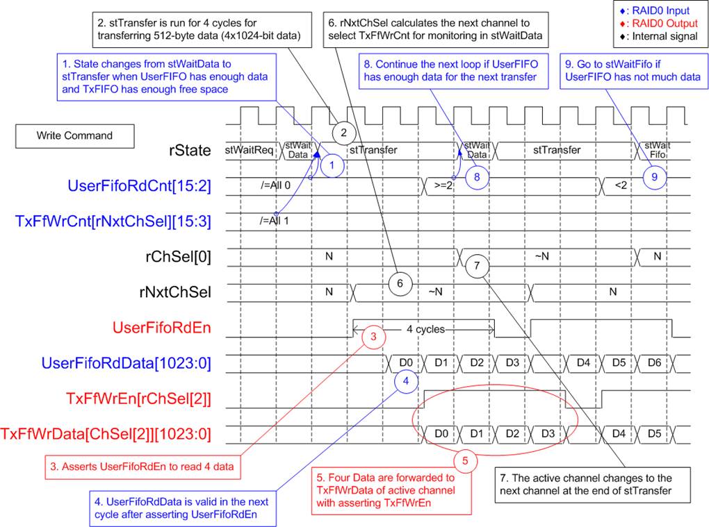
Figure 2‑10 RAID0x2 timing diagram in Write command
When a Write command is sent to RAID0x2, the data is forwarded from UserFIFO (U2IPFIFO) to TxFIFO[0]-[1]. Only one TxFIFO is active at a time to transfer 512-byte data. Following the RAID0 behavior, the active channel is switched to the next channel after completing the transfer of 512-byte data. The sequence of operation is as follows.
1) The core state of the RAID0x2 module is stWaitData. Firstly, it checks the remaining transfer size. If the remaining transfer size is 0, the operation is finished. Otherwise, it monitors UserFifoRdCnt and TxFfWrCnt to ensure that at least 512-byte data is stored in U2IPFIFO and TxFIFO has at least 1024-byte free space. If the FIFOs are ready, the write operation begins.
Note:
i) TxFfWrCnt of two channels are fed to multiplexer to select the active channel. This introduces a one-clock latency compared to UserFifoRdCnt.
ii) rNxtChSel controls TxFfWrCnt and indicates the next active channel for running in stTransfer. After starting the first transfer loop, rNxtChSel is incremented to scan the free space size of the next active channel FIFO.
2) The state machine enters stTransfer to start forwarding the write data from user logic to TxFIFO. This state is active for 4 clock cycles.
3) During the stTransfer state, UserFifoRdEn is asserted to read 512-byte data from UserFIFO.
4) The read data (UserFifoRdData) becomes valid in the next cycle after UserFifoRdEn is asserted.
5) The data is forwarded to the TxFIFO of the active channel, selected by rChSel[2], which is two-clock latency signal of rChSel[0].
Note: rChSel[0] indicates the active channel for data transfer in the stTransfer state.
6) In stTransfer state, rNxtChSel calculates the next active channel based on rChSel[0]. rNxtChSel is applied to select the active channel for reading TxFfWrCnt, which is read in the stWaitData state.
7) After finishing 512-byte data transfer, the active channel for data transfer (rChSel[0]) is incremented.
8) To reduce the overhead time for running the next transfer loop, UserFifoRdCnt is monitored in the stTransfer state. If the read counter indicates at least 2x512-byte data is stored in the FIFO, the new transfer loop starts in the next cycle by transitioning back to the stWaitData state and returning to step 1. Otherwise, the next state is stWaitFifo, as described in step 9.
9) stWaitFIFO is designed to wait until the current data transfer is completed and UserFifoRdCnt becomes valid for monitoring. After waiting for three clock cycles, the state enters stWaitData to continue the next transfer or complete the operation.
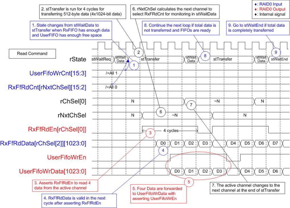
Figure 2‑11 RAID0x2 timing diagram in Read command
When a Read command is sent to RAID0x2, the data is forwarded from RxFIFO[0]-[1] to IP2UFIFO. Similar to the Write command, only one RxFIFO is active at a time to transfer 512-byte data. Following the RAID0 behavior, the active channel is switched to the next channel after completing the transfer of 512-byte data. The sequence of operation is as follows.
1) The state �stWaitData� is responsible for checking the remaining transfer length and two FIFO status signals: RxFfRdCnt and UserFifoWrCnt. It needs to ensure that at least 512-byte data is stored in RxFIFO and IP2UFIFO has at least 1024-byte free space. If the FIFOs are ready and the remaining transfer size is not 0, the read operation begins.
Note:
i) RxFfRdCnt of two channels are fed to multiplexer to select the active channel. This introduces a one-clock latency compared to UserFifoWrCnt.
ii) rNxtChSel controls RxFfRdCnt and indicates the next active channel for running in stTransfer.
2) The state machine enters stTransfer to start forwarding the read data from RxFIFO to user logic.
3) RxFfRdEn of the active channel, selected by rChSel[0], is asserted to 1b for 4 clock cycles to read 512-byte data from RxFIFO.
4) Following the standard FIFO behavior, the Read data (RxFfRdData) becomes valid in the next cycle after asserting the Read enable (RxFfRdEn).
5) The data of the active channel, selected by rChSel[2], is forwarded to the UserFIFO.
Note: rChSel[2] is ChSel[0] signal with a two-clock latency.
6) In stTransfer state, rNxtChSel calculates the next active channel based on rChSel[0]. rNxtChSel is applied to select the active channel for reading RxFfRdCnt, which is read in the stWaitData.
7) After finishing 512-byte data transfer, the active channel for data transfer (rChSel[0]) is incremented.
8) If there is remaining transfer length, the state returns to stTransfer to start a new data transfer, similar to step 2. Otherwise, the next state is stWaitEnd, as described in step 9.
9) If all data has been completely transferred, the state enters stWaitEnd to wait until all devices finish their operation by de-asserting the Busy signal to 0b.
2.3 CPU and Peripherals
The CPU system uses a 32-bit Avalon-MM bus as the interface to access peripherals such as the Timer and JTAG UART. The system also integrates an additional peripheral to access NVMeRAID0x2IP test logic by assigning a unique base address and address range. To support CPU read and write operations, the hardware logic must comply with the Avalon-MM bus standard. Avl2Reg module, as shown in Figure 2‑12, is designed to connect the CPU system via the Avalon-MM interface, in compliance with the standard.
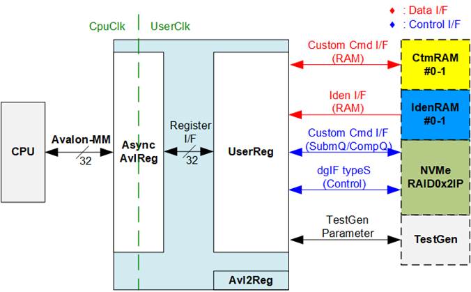
Figure 2‑12 CPU and peripherals hardware
Avl2Reg consists of AsyncAvlReg and UserReg. AsyncAvlReg converts Avalon-MM signals into a simple Register interface with a 32-bit data bus size, similar to the Avalon-MM data bus size. It also includes asynchronous logic to handle clock domain crossing between the CpuClk and UserClk domains.
UserReg includes the register file of the parameters and the status signals of other modules in the test system, including the CtmRAMs, IdenRAMs, NVMeRAID0x2IP, and TestGen. More details of AsyncAvlReg and UserReg are explained below.
2.3.1 AsyncAvlReg
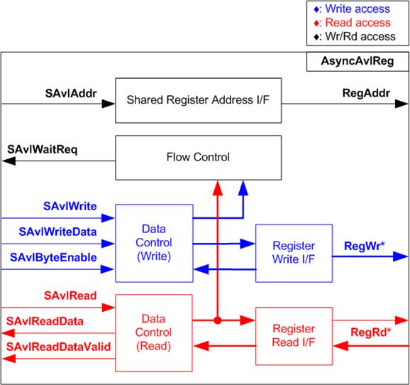
Figure 2‑13 AsyncAxiReg Interface
The Avalon-MM bus interface signal can be grouped into three categories: Write channel (blue), Read channel (red), and Shared control channel (black). More details about the Avalon-MM interface specification can be found in the following document.
https://www.intel.com/content/dam/www/programmable/us/en/pdfs/literature/manual/mnl_avalon_spec.pdf
According to Avalon-MM specification, only one command (write or read) can be executed at a time. AsyncAvlReg�s logic is divided into three groups: Write control logic, Read control logic, and Flow control logic. The flow control logic asserts SAvlWaitReq to hold the next request from the Avalon-MM interface if the current request has not finished. Write control and Write data I/F of the Avalon-MM bus are latched and transferred to the Write register interface with clock domain crossing registers. Similarly, Read control I/F are latched and transferred to be Read register interface. Afterward, the data returned from Register Read I/F is transferred to Avalon-MM bus with using clock domain crossing registers. The Address I/F of Avalon-MM is also latched and transferred to the Address register interface.
The Register interface is compatible with the single-port RAM interface for write transactions. However, the read transaction of the Register interface is slightly modified from RAM interface by adding RdReq and RdValid signals to control the read latency time. Since the address of the Register interface is shared for write and read transactions, the user cannot write and read the register at the same time. The timing diagram of the Register interface is shown in Figure 2‑14.
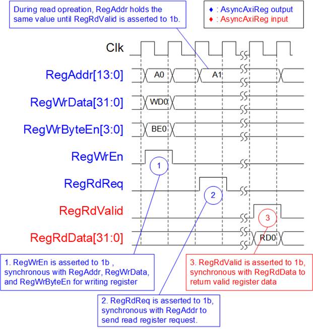
Figure 2‑14 Register interface timing diagram
1) Timing diagram to write register is similar to that of a single-port RAM. The RegWrEn signal is set to 1b, along with a valid RegAddr (Register address in 32-bit units), RegWrData (write data for the register), and RegWrByteEn (write byte enable). The byte enable consists of four bits that indicate the validity of the byte data. For example, bit[0], [1], [2], and [3] are set to 1b when RegWrData[7:0], [15:8], [23:16], and [31:24] are valid, respectively.
2) To read register, AsyncAvlReg sets the RegRdReq signal to 1b with a valid value for RegAddr. The 32-bit data is returned after the read request is received. The slave detects the RegRdReq signal being set to start the read transaction. In the read operation, the address value (RegAddr) remains unchanged until RegRdValid is set to 1b. The address can then be used to select the returned data using multiple layers of multiplexers.
3) The slave returns the read data on RegRdData bus by setting the RegRdValid signal to 1b. After that, AsyncAvlReg forwards the read value to the SAvlRead interface.
2.3.2 UserReg
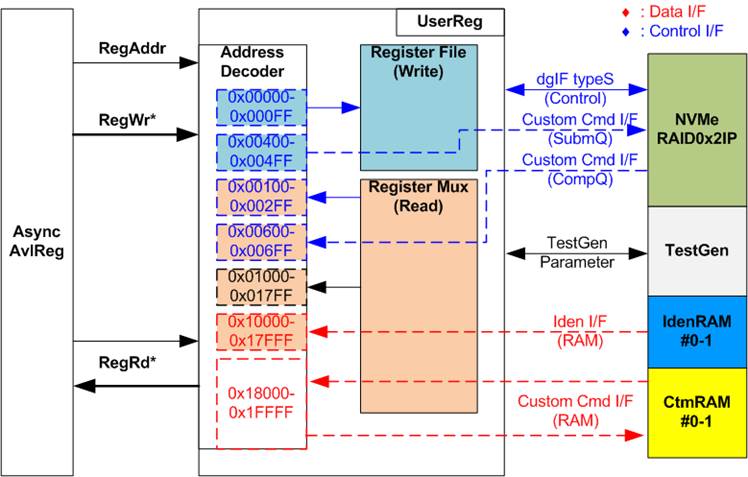
Figure 2‑15 UserReg Interface
The UserReg module consists of an Address decoder, a Register File, and a Register Mux. The Address decoder decodes the address requested by AsyncAvlReg and selects the active register for either write or read transactions. The assigned address range in UserReg is divided into six areas, as shown in Figure 2‑15.
1) 0x00000 � 0x000FF: mapped to set the command with the parameters of TestGen and NVMeRAID0x2IP. This area is write-access only.
2) 0x00400 � 0x004FF: mapped to set the parameters for the Custom command interface of NVMeRAID0x2IP. This area is write-access only.
3) 0x00100 � 0x002FF: mapped to read the status signals of NVMeRAID0x2IP. This area is read-access only.
4) 0x00600 � 0x006FF: mapped to read the status of Custom command interface (NVMeRAID0x2IP). This area is read-access only.
5) 0x01000 � 0x017FF: mapped to read the status signals of TestGen. This area is read-access only.
6) 0x10000 � 0x17FFF: mapped to read data from IdenRAM. This area is read-access only.
7) 0x18000 � 0x1FFFF: mapped to write or read data using Custom command RAM interface. This area allows both write-access and read access. However, the demo shows only read-access by running the SMART command.
The Address decoder decodes the upper bits of RegAddr to select the active hardware (NVMeRAID0x2IP, TestGen, IdenRAM, or CtmRAM). The Register File within UserReg has a 32-bit bus size, so the write byte enable (RegWrByteEn) is not used in the test system, and the CPU uses a 32-bit pointer to set the hardware register.
To read the register, multi-level multiplexers (mux) select the data to return to the CPU by using the address. The lower bits of RegAddr are fed to the submodule to select the active data from each submodule. While the upper bits are used in UserReg to select the returned data from each submodule. The latency time of read data equals to three clock cycles, so RegRdValid is created by RegRdReq, with three D Flip-flops asserted. More details of the address mapping within the UserReg module are shown in Table 2‑2.
Table 2‑2 Register Map
|
Address |
Register Name |
Description |
|
Wr/Rd |
(Label in �nvmeraid0g5test.c�) |
|
|
0x00000 � 0x000FF: Control signals of NVMeRAID0x2IP and TestGen (Write access only) |
||
|
BA+0x00000 |
User Address (Low) Reg |
[31:0]: Input to be bit[31:0] of start address in 512-byte unit (UserAddr[31:0] of dgIF typeS for NVMeRAID0x2IP) |
|
(USRADRL_INTREG) |
||
|
BA+0x00004 |
User Address (High) Reg |
[15:0]: Input to be bit[47:32] of start address in 512-byte unit (UserAddr[47:32] of dgIF typeS for NVMeRAID0x2IP) |
|
(USRADRH_INTREG) |
||
|
BA+0x00008 |
User Length (Low) Reg |
[31:0]: Input to be bit[31:0] of transfer length in 512-byte unit (UserLen[31:0] of dgIF typeS for NVMeRAID0x2IP) |
|
(USRLENL_INTREG) |
||
|
BA+0x0000C |
User Length (High) Reg |
[15:0]: Input to be bit[47:32] of transfer length in 512-byte unit (UserLen[47:32] of dgIF typeS for NVMeRAID0x2IP) |
|
(USRLENH_INTREG) |
||
|
BA+0x00010 |
User Command Reg |
[2:0]: Input to be user command (UserCmd of dgIF typeS for NVMeRAID0x2IP) 000b: Identify, 001b: Shutdown, 010b: Write RAID, 011b: Read RAID, 100b: SMART/Secure Erase, 110b: Flush, 101b/111b: Reserved. When this register is written, the command request is sent to NVMeRAID0x2IP to start the operation. |
|
(USRCMD_INTREG) |
||
|
BA+0x00014 |
Test Pattern Reg |
[2:0]: Select test pattern 000b-Increment, 001b-Decrement, 010b-All 0, 011b-All 1, 100b-LFSR |
|
(PATTSEL_INTREG) |
||
|
BA+0x00020 |
NVMe Timeout Reg |
[31:0]: Input to be timeout value of all NVMe-IPs (TimeOutSet[31:0] of NVMe-IP) |
|
(NVMTIMEOUT_INTREG) |
||
|
0x00100 � 0x002FF: Status signals of NVMeRAID0x2IP (Read access only) |
||
|
BA+0x0100 |
User Status Reg |
[0]: UserBusy of dgIF typeS for NVMeRAID0x2IP (0b: Idle, 1b: Busy) [1]: UserError of dgIF typeS for NVMeRAID0x2IP (0b: Normal, 1b: Error) [2]: Data verification fail in TestGen (0b: Normal, 1b: Error) |
|
(USRSTS_INTREG) |
||
|
BA+0x0104 |
Total device size (Low) Reg |
[31:0]: Mapped to LBASize[31:0] of NVMeRAID0x2IP |
|
(LBASIZEL_INTREG) |
||
|
BA+0x0108 |
Total device size (High) Reg |
[15:0]: Mapped to LBASize[47:32] of NVMeRAID0x2IP [31]: Mapped to LBAMode of NVMeRAID0x2IP |
|
(LBASIZEH_INTREG) |
||
|
(BA+0x0120)- (BA+0x0127) |
User Error Type CH#0-#1 Reg |
[31:0]: Mapped to UserErrorType of NVMe-IP 0x0120: NVMe-IP#0, 0x0124: NVMe-IP#1, |
|
(USRERRTYPECH0-1_INTREG) |
||
|
(BA+0x0140)- (BA+0x0147) |
PCIe Status CH#0-#1 Reg |
[0]: PCIe linkup status from PCIe hard IP (0b: No linkup, 1b: linkup) [3:2]: Two lower bits to show PCIe link speed. Two upper bits are bit[17:16]. (0000b: Not linkup, 0001b: PCIe Gen1, 0010b: PCIe Gen2, 0011b: PCIe Gen3, 0111b: PCIe Gen4, 1111b: PCIe Gen5) [6:4]: PCIe link width status from PCIe hard IP (001b: 1-lane, 010b: 2-lane, 100b: 4-lane) [13:8]: Current LTSSM State of PCIe hard IP. Please see more details of LTSSM value in Avalon-ST PCIe Hard IP datasheet [17:16]: Two upper bit to show PCIe link speed. Two lower bits are bit[3:2]. 0x0140: NVMe-IP#0, 0x0144: NVMe-IP#1 |
|
(PCIESTSCH0-1_INTREG) |
||
|
(BA+0x0160)- (BA+0x0167) |
Completion Status CH#0-#1 Reg |
[15:0]: Status from Admin completion (AdmCompStatus[15:0] of NVMe-IP) [31:16]: Status from I/O completion (IOCompStatus[15:0] of NVMe-IP) 0x0160: NVMe-IP#0, 0x0164: NVMe-IP#1 |
|
(COMPSTSCH0-1_INTREG) |
||
|
(BA+0x0180)- (BA+0x0187) |
NVMe CAP CH#0-#1 Reg |
[31:0]: Mapped to NVMeCAPReg[31:0] of NVMe-IP 0x0180: NVMe-IP#0, 0x0184: NVMe-IP#1 |
|
(NVMCAPCH0-1_INTREG) |
||
|
(BA+0x00200)- (BA+0x0021F) |
NVMe IP Test pin CH#0-#1 Reg |
Mapped to TestPin[127:0] of NVMe-IP 0x0200: Bit[31:0] of NVMe-IP#0, 0x204: Bit[63:32] of NVMe-IP#0 0x0208: Bit[95:64] of NVMe-IP#0, 0x20C: Bit[127:96] of NVMe-IP#0 0x0210 � 0x021F: TestPin[127:0] of NVMe-IP#1 |
|
(NVMTESTPIN0-3CH0-1_INTREG) |
||
|
Address |
Register Name |
Description |
|
Wr/Rd |
(Label in �nvmeraid0g5test.c�) |
|
|
0x00400 � 0x005FF: Custom command of NVMeRAID0x2IP |
||
|
(BA+0x00400)- (BA+0x0047F) |
Custom Submission Queue CH#0�#1 Reg |
[31:0]: Submission queue entry of SMART, Flush, or Secure Erase command. Input to be CtmSubmDW0-DW15 of NVMe-IP#0-#1. 0x400: DW0, 0x404: DW1, �, 0x43C: DW15 of NVMe-IP#0 0x440: DW0, 0x444: DW1, �, 0x47C: DW15 of NVMe-IP#1 |
|
Wr |
(CTMSUBMQ0-1_STRUCT) |
|
|
(BA+0x00600)- (BA+0x0061F) |
Custom Completion Queue CH#0�#1 Reg |
[31:0]: CtmCompDW0-DW3 output from NVMe-IP#0-#1 successively. 0x600: DW0, 0x604: DW1, �, 0x60C: DW3 of NVMe-IP#0 0x610: DW0, 0x614: DW1, �, 0x61C: DW3 of NVMe-IP#1 |
|
Rd |
(CTMCOMPQ0-1_STRUCT) |
|
|
BA+0x00800 |
IP Version Reg |
[31:0]: Mapped to IPVersion[31:0] of NVMe-IP |
|
Rd |
(IPVERSION_INTREG) |
|
|
0x01000 � 0x017FF: Status signals of TestGen (Read access only) |
||
|
BA+0x01000 |
Data Failure Address(Low) Reg |
[31:0]: Bit[31:0] of the byte address of the 1st failure when executing a Read command |
|
(RDFAILNOL_INTREG) |
||
|
BA+0x01004 |
Data Failure Address(High) Reg |
[24:0]: Bit[56:32] of the byte address of the 1st failure when executing a Read command |
|
(RDFAILNOH_INTREG) |
||
|
BA+0x01008 |
Current test byte (Low) Reg |
[31:0]: Bit[31:0] of the current test data size in TestGen module |
|
(CURTESTSIZEL_INTREG) |
||
|
BA+0x0100C |
Current test byte (High) Reg |
[24:0]: Bit[56:32] of the current test data size in TestGen module |
|
(CURTESTSIZEH_INTREG) |
||
|
(BA+0x01200)- (BA+0x0127C) |
Expected value Word0-31 Reg |
1024-bit of the expected data at the 1st failure data in Read command 0x1200: Bit[31:0], 0x1204: Bit[63:32], �, 0x127C: Bit[1023:992] |
|
(EXPPATW0-W31_INTREG) |
||
|
(BA+0x01400)- (BA+0x0147C) |
Read value Word0-31 Reg |
1024-bit of the read data at the 1st failure data in Read command 0x1400: Bit[31:0], 0x1404: Bit[63:32], �, 0x147C: Bit[1023:992] |
|
(RDPATW0-W31_INTREG) |
||
|
0x10000 � 0x1FFFF: Identify RAM and Custom RAM |
||
|
(BA+0x10000) � (BA+0x10FFF) |
Identify Controller Data CH#0 |
4Kbyte Identify controller data of NVMe-IP#0 |
|
Rd |
IDENCTRL0_CHARREG |
|
|
(BA+0x11000) � (BA+0x11FFF) |
Identify Namespace Data CH#0 |
4Kbyte Identify namespace data of NVMe-IP#0
|
|
Rd |
IDENNAME0_CHARREG |
|
|
(BA+0x12000) � (BA+0x13FFF) |
Identify Controller Data CH#1 and Identify Namespace Data CH#1 |
0x12000-0x12FFF: 4Kbyte Identify controller data of NVMe-IP#1 0x13000-0x13FFF: 4Kbyte Identify namespace data of NVMe-IP#1 |
|
Rd |
IDENCTRL/NAME1_CHARREG |
|
|
(BA+0x18000) � (BA+0x1BFFF) |
Custom command Ram CH#0-#1
|
8K byte CtmRAM interface of NVMe-IP#0-#1 for storing 512-byte data output from SMART command. 0x18000-0x19FFF: NVMe-IP#0 0x1A000-0x1BFFF: NVMe-IP#1 |
|
Wr/Rd |
(CTMRAM0-1_CHARREG) |
|
3 CPU Firmware
3.1 Test firmware (nvmeraid0g5test.c)
The CPU follows these steps upon system startup to complete the initialization process.
1) Initializes JTAG UART and Timer parameters.
2) Waits until the PCIe connection become active (PCIESTSCH0-1_INTREG[0]= 1b).
3) Waits until NVMeRAID0x2IP completes its own initialization process (USRSTS_INTREG[0]=0b). The error message is displayed and the process stops when some errors are found.
4) CPU displays PCIe link status (the number of PCIe lanes and the PCIe speed) of each channel by reading PCIESTSCH0-1_INTREG[17:2].
5) CPU displays the main menu. There are seven menus for running seven commands of RAID0 module, i.e., Identify, Write, Read, SMART, Flush, Secure Erase, and Shutdown.
More details of the operation flow in each command are described as follows.
3.1.1 Identify command
The sequence for the firmware when the Identify command is selected by user is as follows.
1) Set USRCMD_INTREG[2:0]=000b to send the Identify command request to NVMeRAID0x2IP. The busy flag (USRSTS_INTREG[0]) will then change from 0b to 1b.
2) The CPU waits until the operation is completed or an errors is detected by monitoring USRSTS_INTREG[1:0].
· If bit[0] is de-asserted to 0b after the operation is finished, the data of Identify command returned by NVMe-IP will be stored in IdenRAM.
· If bit[1] is asserted to 1b, indicating an error, the error message will be displayed on the console with details decoded from USRERRTYPECH0-1_INTREG[31:0]. The process will then stop.
3) Once the busy flag (USRSTS_INTREG[0]) is de-asserted to 0b, the CPU will display decoded information from IdenRAM (IDENCTRL0-1_CHARREG). This information includes the model name of SSD#0/#1 and the device details obtained from the output signals of NVMeRAID0x2, such as the device capacity (LBASIZEL/H_INTREG), LBA mode (LBASIZEH_INTREG[31]), and support for Secure Erase command. If the LBA size of NVMeRAID0x2IP is 4 Kbytes, which is not supported by the current RAID0 controller design, the process will be halted and the error message will be displayed.
3.1.2 Write/Read command
The sequence for the firmware when the Write/Read command is selected is as follows.
1) Receive start address, transfer length, and test pattern from JTAG UART. If any inputs are invalid, the operation will be cancelled.
2) After obtaining all the inputs, set them to USRADRL/H_INTREG, USRLENL/H_INTREG, and PATTSEL_INTREG.
3) To execute the Write or Read command, set USRCMD_INTREG[2:0]= 010b or 011b, respectively. This sends the command request to the NVMeRAID0x2IP. Once the command is issued, the busy flag of NVMeRAID0x2IP (USRSTS_INTREG[0]) will change from 0b to 1b.
4) The CPU waits until the operation is completed or an errors (excluding verification error) is detected by monitoring USRSTS_INTREG[2:0].
· If bit[0] is de-asserted to 0b after the operation is finished, the CPU will then proceed to the next step.
· If bit[1] is asserted to 1b, indicating an error, the error message will be displayed on the console with details decoded from USRERRTYPECH0-1_INTREG[31:0]. The process will then stop.
· If bit[2] is asserted to 1b, indicating a data verification fails, the verification error message will be displayed on the console, but the CPU will continue to run until the operation is complete or the user cancels the operation by pressing any key.
While the command is running, the current transfer size, read from
CURTESTSIZEL/H_INTREG, will be displayed every second.
5) After the busy flag (USRSTS_INTREG[0]) is de-asserted to 0b, CPU will calculate and display the test result on the console including the total time usage, total transfer size, and transfer speed.
3.1.3 SMART Command,
The sequence of the firmware when the SMART command is selected is as follows.
1) The 16-Dword of Submission Queue entry (CTMSUBMQ0-1_STRUCT) is set to the SMART command value.
2) Set USRCMD_INTREG[2:0]=100b to send the SMART command request to NVMeRAID0x2IP. The busy flag (USRSTS_INTREG[0]) will then change from 0b to 1b.
3) The CPU waits until the operation is completed or an error is detected by monitoring USRSTS_INTREG[1:0].
· If bit[0] is de-asserted to 0b after the operation is finished, the data of SMART command returned by NVMe IP will be stored in CtmRAM.
· If bit[1] is asserted to 1b, indicating an error, the error message will be displayed on the console with details decoded from USRERRTYPECH0-1_INTREG[31:0]. The process will then stop.
4) After the busy flag (USRSTS_INTREG[0]) is de-asserted to 0b, the CPU will display information decoded from CtmRAM (CTMRAM0-1_CHARREG), i.e., Remaining Life, Percentage Used, Temperature, Total Data Read, Total Data Written, Power On Cycles, Power On Hours, and Number of Unsafe Shutdown.
For more information on the SMART log, refer to the NVM Express Specification.
https://nvmexpress.org/resources/specifications/
3.1.4 Flush Command
The sequence of the firmware when the Flush command is selected is as follows.
1) The 16-Dword of Submission Queue entry (CTMSUBMQ0-1_STRUCT) is set to the Flush command value.
2) Set USRCMD_INTREG[2:0]=110b to send Flush command request to NVMeRAID0x2IP. The busy flag of NVMeRAID0x2IP (USRSTS_INTREG[0]) will then change from 0b to 1b
3) The CPU waits until the operation is completed or an error is detected by monitoring USRSTS_INTREG[1:0].
· If bit[0] is de-asserted to 0b after the operation is finished, the CPU will then return to the main menu.
· If bit[1] is asserted to 1b, indicating an error , the error message will be displayed on the console with details decoded from USRERRTYPECH0-1_INTREG[31:0]. The process will then stop.
3.1.5 Secure Erase Command
The sequence of the firmware when the Secure Erase command is selected is as follows.
1) The 16-Dword of Submission Queue entry (CTMSUBMQ0-1_STRUCT) is set to the Secure Erase command value.
2) Set NVMTIMEOUT_INTREG to 0 to disable timer to prevent the timeout error.
3) Set USRCMD_INTREG[2:0]=100b to send Secure Erase command request to NVMeRAID0x2IP. The busy flag of NVMeRAID0x2IP (USRSTS_INTREG[0]) will then change from 0b to 1b.
4) The CPU waits until the operation is completed or an error is detected by monitoring USRSTS_INTREG[1:0].
· If bit[0] is de-asserted to 0b after the operation is finished, the CPU will then proceed to the next step.
· If bit[1] is asserted to 1b, indicating an error, the error message will be displayed on the console with the details decoded from USRERRTYPECH0-1_INTREG[31:0]. The process will then stop.
5) After completing the command, the timer is re-enabled to generate timeout error in NVMe-IP by setting NVMTIMEOUT_INTREG to the default value.
3.1.6 Shutdown Command
The sequence of the firmware when the Shutdown command is selected is as follows.
1) Set USRCMD_INTREG[2:0]=001b to send the Shutdown command request to NVMeRAID0x2IP. The busy flag of NVMeRAID0x2IP (USRSTS_INTREG[0]) will then change from 0b to 1b.
2) The CPU waits until the operation is completed or an error is detected by monitoring USRSTS_INTREG[1:0].
· If bit[0] is de-asserted to 0b after the operation is finished, the CPU will then proceed to the next step.
· If bit[1] is asserted to 1b, indicating an error, the error message will be displayed on the console with details decoded from USRERRTYPECH0-1_INTREG[31:0]. The process will then stop.
3) After Shutdown command completes, both the SSD and all NVMe-IPs will become inactive and the CPU will be unable to receive any new commands from the user. To continue testing, the user must power off and power on the system.
3.2 Function list in Test firmware
|
int exec_ctm(unsigned int user_cmd) |
|
|
Parameters |
user_cmd: 4-SMART/Secure Erase command, 6-Flush command |
|
Return value |
0: No error, -1: Some errors are found in NVMeRAID0x2IP |
|
Description |
Execute SMART command as outlined in section 3.1.3 (SMART Command,), execute Flush command as outlined in section 3.1.4 (Flush Command), or execute Secure Erase command as outlined in section 3.1.5 (Secure Erase Command). |
|
unsigned long long get_cursize(void) |
|
|
Parameters |
None |
|
Return value |
Read value of CURTESTSIZEH/L_INTREG |
|
Description |
Read the value of CURTESTSIZEH/L_INTREG and return it as the result of the function. |
|
int get_param(userin_struct* userin) |
|
|
Parameters |
userin: Three inputs from user, i.e., start address, total length in 512-byte unit, and test pattern |
|
Return value |
0: Valid input, -1: Invalid input |
|
Description |
Receive the input parameters from the user and verify the value. When the input is invalid, the function returns -1. Otherwise, all inputs are updated to userin parameter. |
|
void iden_dev(void) |
|
|
Parameters |
None |
|
Return value |
None |
|
Description |
Execute Identify command as outlined in section 3.1.1 (Identify command). |
|
int setctm_erase(void) |
|
|
Parameters |
None |
|
Return value |
0: No error, -1: Some errors are found in NVMeRAID0x2IP |
|
Description |
Set Secure Erase command to CTMSUBMQ0-1_STRUCT and call exec_ctm function to execute Secure Erase command. |
|
int setctm_flush(void) |
|
|
Parameters |
None |
|
Return value |
0: No error, -1: Some errors are found in NVMeRAID0x2IP |
|
Description |
Set Flush command to CTMSUBMQ0-1_STRUCT and call exec_ctm function to start Flush command. |
|
int setctm_smart(void) |
|
|
Parameters |
None |
|
Return value |
0: No error, -1: Some errors are found in NVMeRAID0x2IP |
|
Description |
Set SMART command to CTMSUBMQ0-1_STRUCT and call exec_ctm function to start SMART command. Finally, decode and display SMART information on the console. |
|
void show_error(void) |
|
|
Parameters |
None |
|
Return value |
None |
|
Description |
Read USRERRTYPECH0-1_INTREG, decode the error flag, and display the corresponding error message. Also, call show_pciestat function to check the hardware�s debug signals. |
|
void show_pciestat(unsigned int channel) |
|
|
Parameters |
Channel: Channel of PCIe status to display on the console |
|
Return value |
None |
|
Description |
Read PCIESTSCH0/1_INTREG until the read value from two read times is stable. After that, display the read value on the console. Also, debug signal is read by NVMTESTPIN0-3CH0-1_INTREG. |
|
void show_result(void) |
|
|
Parameters |
None |
|
Return value |
None |
|
Description |
Print total size by calling get_cursize and show_size function. After that, calculate total time usage from global parameters (timer_val and timer_upper_val) and then display in usec, msec, or sec unit. Finally, transfer performance is calculated and displayed in MB/s unit. |
|
void show_size(unsigned long long size_input) |
|
|
Parameters |
size_input: Transfer size to display on the console. |
|
Return value |
None |
|
Description |
Calculate and display the input value in Mbyte or Gbyte unit. The display format allows for representing data sizes with up to 6 digits and 3 decimal places. This means that the maximum value that can be shown is 999,999.999 GB. |
|
void show_smart_hex16byte(volatile unsigned char *char_ptr) |
|
|
Parameters |
*char_ptr: Pointer of 16-byte SMART data |
|
Return value |
None |
|
Description |
Display 16-byte SMART data as hexadecimal unit. |
|
void show_smart_int8byte(volatile unsigned char *char_ptr) |
|
|
Parameters |
*char_ptr: Pointer of 8-byte SMART data |
|
Return value |
None |
|
Description |
When the input value is less than 4 billion (32-bit), the 8-byte SMART data is displayed in decimal units. If the input value exceeds this limit, an overflow message is displayed. |
|
void show_smart_size8byte(volatile unsigned char *char_ptr) |
|
|
Parameters |
*char_ptr: Pointer of 8-byte SMART data |
|
Return value |
None |
|
Description |
Display 8-byte SMART data as GB or TB unit. When the input value is more than limit (500 PB), the overflow message is displayed instead. |
|
void show_vererr(void) |
|
|
Parameters |
None |
|
Return value |
None |
|
Description |
Read RDFAILNOL/H_INTREG (error byte address), EXPPATW0-W31_INTREG (expected value), and RDPATW0-W31_INTREG (read value) to display verification error details on the console. |
|
void shutdown_dev(void) |
|
|
Parameters |
None |
|
Return value |
None |
|
Description |
Execute Shutdown command as outlined in section 3.1.6 (Shutdown Command) |
|
int wrrd_dev(unsigned int user_cmd) |
|
|
Parameters |
user_cmd: 2-Write command, 3-Read command |
|
Return value |
0: No error, -1: Receive invalid input or some errors are found. |
|
Description |
Execute Write command or Read command as outlined in section 3.1.2 (Write/Read command). Show_result function is called to calculate and display transfer performance in Write/Read command. |
4 Example Test Result
Figure 4‑1 illustrates the result of executing the RAID0x2 demo, using two SSDs: the 2TB CFD Gaming PG5NFZ SSD and the 2TB AORUS Gen5 10000 SSD. Since both SSDs utilize the same controller, their characteristics are expected to be similar. The result was measured using Write and Read commands, utilizing an LFSR test data pattern and a transfer size of 256 GB.
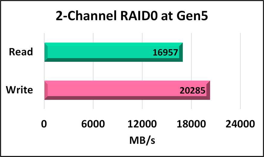
Figure 4‑1 Performance of 2-ch RAID0 demo by using two Gen5 SSDs
Utilizing the Agilex 7 I-Series board with PCIe Gen5, the system demonstrates remarkable performance levels. The write speed reaches approximately 20,000 Mbyte/sec, while the read speed achieves around 16,900 Mbyte/sec.
5 Revision History
|
Revision |
Date |
Description |
|
1.0 |
7-Jul-23 |
Initial version release |
Copyright: 2023 Design Gateway Co,Ltd.