4-ch RAID0 Design (NVMe-IP for AGL) reference design manual
Rev1.1 15-Aug-23
2.2.2 Avalon-ST Intel Hard IP for PCIe (P-Tile)
3.1 Test firmware (nvmeraid0g4test.c)
3.2 Function list in Test firmware
1 Introduction
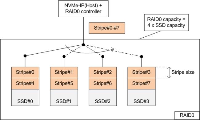
Figure 1‑1 RAID0 by 4 SSDs data format
RAID0 system uses multiple storages to extend total storage capacity and increase write/read performance. Assumed that total number of devices connecting in RAID0 system is N, total storage capacity of RAID0 is equal to N times of one device capacity. Write and read performance of RAID0 are almost equal to N times of one device performance.
Data format of RAID0 is shown in Figure 1‑1. Data stream of the host side is split into a small stripe for transferring with one SSD at a time. Stripe size is the data size transferring with one SSD before switching to other SSDs. In RAID0 reference design, stripe size is equal to 512-byte.
In this demo, four SSDs are connected in the system. It is recommended to use the same SSD model for all channels to match the characteristic and achieve the best performance. As a result, the total capacity is equal to four times of one SSD and the write/read performance are almost four times of one SSD performance.
The demo uses FIFO implemented by Block Memory to be the buffer which has smaller size than using DDR. Therefore, the buffer is sometimes not ready to transfer data when SSD pauses data transmission for long time in Write process. Test performance in the demo is average speed, not sustain rate. User can modify RAID0 reference design by increasing the numbers of SSD to achieve the better performance and the bigger capacity. Furthermore, user can add DDR to be data buffer in the system for supporting high-speed transferring as sustain rate.
Before running the reference design, it is recommended to read NVMe-IP for Agilex datasheet and single channel demo from following link.
https://dgway.com/products/IP/NVMe-IP/dg_nvme_datasheet_agl.pdf
https://dgway.com/products/IP/NVMe-IP/dg_nvmeip_refdesign_agl.pdf
https://dgway.com/products/IP/NVMe-IP/dg_nvmeip_instruction_agl.pdf
2 Hardware overview
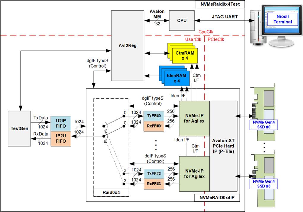
Figure 2‑1 RAID0x4 demo system by using NVMe-IP
The hardware system can be divided to three groups, i.e., TestGen, NVMeRAID0x4, and CPU. First, TestGen is the test logic to generate and verify test data stream with NVMeRAID0x4 through U2IPFIFO/IP2UFIFO. Second, NVMeRAID0x4 consists of the Raid0x4, four NVMe-IPs, and one PCIe hard IP (P-Tile Avalon-ST PCIe hard IP) that is configured to be 4x4-lane PCIe Gen4. Data format in four NVMe SSDs is arranged as RAID0, controlled by Raid0x4 module. Each NVMe SSD must directly connect to PCIe hard IP without PCIe switch. Last, CPU and Avl2Reg are designed to interface with user through JTAG UART. User sets test parameters and monitors hardware status through the console. When CPU detects the command request from the user, CPU handles the hardware to run the command until finishing.
There are three clock domains displayed in Figure 2‑1, i.e., CpuClk, PCIeClk, and UserClk. First, CpuClk is the clock domain of CPU and its peripherals. This clock must be stable clock which may be different from the clock of other hardwares. Second, PCIeClk is the clock output from PCIe hard IP that is configured to be 500 MHz. The PCIe hard IP is set to 4-lane PCIe Gen4 and uses 128-bit Avalon-ST interface. Last, UserClk is the example user clock for running all user logics such as Raid0x4, NVMe-IP, RAM, FIFO, and TestGen. According to NVMe-IP for Agilex datasheet, clock frequency of UserClk must be more than or equal to a half of PCIeClk frequency, 250 MHz. In this reference design, UserClk is equal to 350 MHz for PCIe Gen4.
There are six memories implemented by Block Memory in the test system � CtmRAM, IdenRAM, TxFIFO, RxFIFO, U2IPFIFO, and IP2UFIFO. CtmRAM stores returned data of each SSD from SMART command while IdenRAM stores returned data from Identify command. When running SMART command or Identify command, the returned data from the command is decoded by CPU which is read through Avl2Reg module by using Avalon-MM interface. TxFIFO and RxFIFO are connected between Raid0x4 and NVMe-IP to convert different data bus size, 1024-bit and 256-bit. U2IPFIFO and IP2UFIFO are connected between TestGen and NVMeRAID0x4 for storing data when running Write command and Read command respectively.
TestGen monitors flow control signals of U2IPFIFO and IP2UFIFO and transfers data when the FIFOs are ready. More details of the hardware are described as follows.
2.1 TestGen
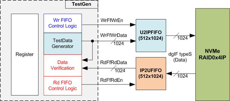
Figure 2‑2 TestGen interface
TestGen module is the test logic to send test data to NVMeRAID0x4 through U2IPFIFO when operating Write command. On the other hand, the test data is applied to be the expected value to verify the read data from NVMeRAID0x4 through IP2UFIFO when operating Read command. Control logic asserts Write enable or Read enable to �1� when the FIFOs are ready. Data bandwidth of TestGen is matched to NVMeRAID0x4 by running at the same clock and the same data bus size. Therefore, U2IPFIFO and IP2UFIFO are always ready for transferring data with NVMeRAID0x4 in Write and Read command. As a result, the test logic shows the best performance to write and read data with the SSD through NVMeRAID0x4.
Register file in the TestGen receives test parameters from user, i.e., total transfer size, transfer direction, and test pattern. To control transfer size, the counter is designed to count total number of transferred data. The details of hardware logic within TestGen module are shown in Figure 2‑3.
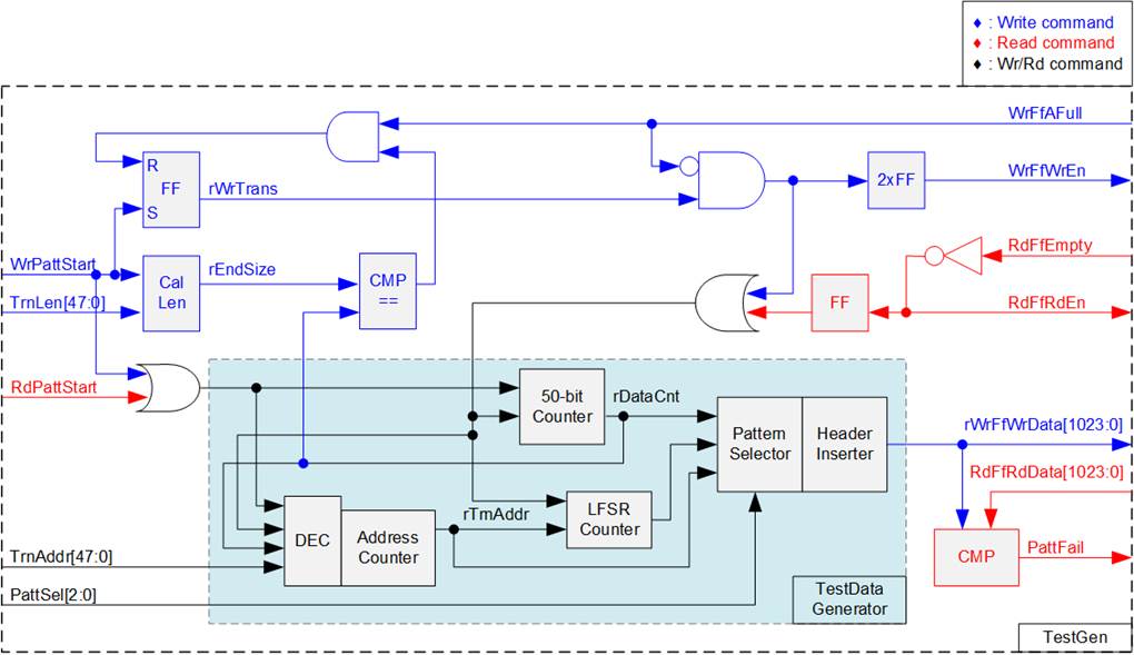
Figure 2‑3 TestGen hardware
As shown in the right side of Figure 2‑3, flow control signals of FIFO are WrFfAFull and RdFfEmpty. When FIFO is almost full during write operation (WrFfAFull=�1�), WrFfWrEn is de-asserted to �0� to pause data sending to FIFO. For read operation, when FIFO has data (RdFfEmpty=�0�), the logic reads data from FIFO to compare with the expected data by asserting RdFfRdEn to �1�.
The logic in the left side of Figure 2‑3 is designed to count transfer size (rDataCnt). When total data count is equal to the end size (rEndSize), set by user, write enable or read enable of FIFO is de-asserted to �0� to finish the operation. The lower side of Figure 2‑3 shows the details to generate test data for writing to FIFO or verifying data from FIFO. There are five patterns to generate, i.e., all zero, all one, 32-bit incremental pattern, 32-bit decremental pattern, and LFSR pattern, selected by Pattern Selector. When creating all-zero or all-one pattern, every bit of data is set to zero or one respectively. While other patterns are designed by separating the data as two parts to create unique test data in every 512-byte data, as shown in Figure 2‑4.
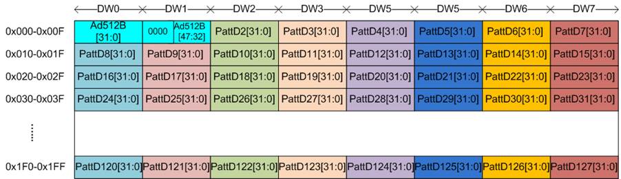
Figure 2‑4 Test pattern format in each 512-byte data for Increment/Decrement/LFSR pattern
512-byte data consists of 64-bit header in Dword#0 and Dword#1 and the test data in remaining words of 512-byte data (Dword#2 � Dword#127). The header is created by using the address in 512-byte unit, Address counter block. The initial value of the address counter is set by user and the value is increased when finishing transferring 512-byte data. Remaining Dwords (DW#2 � DW#127) depends on pattern selector which may be 32-bit incremental data, 32-bit decremental data, or LFSR counter. 32-bit incremental data is designed by using 50-bit counter. The decremental data can be designed by connecting NOT logic to increment data.
The LFSR pattern is designed by using LFSR counter. The equation of LFSR is x^31 + x^21 + x + 1. To implement 1024-bit LFSR pattern, the data is split to be eight sets of 128-bit data which uses the different start value as shown in Figure 2‑5.
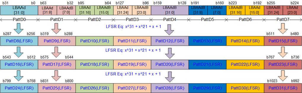
Figure 2‑5 1024-bit LFSR Pattern in TestGen
By using look-ahead technique, one cycle generates four 32-bit LFSR data or 128-bit data, the same color in Figure 2‑5. The start value of each data set is designed by using combination signal of 32-bit LBA address (LBAAd) and NOT logic of LBA address (LBAAdB).
Test data is fed to be write data to the FIFO or the expected data for verifying with the read data from FIFO. Fail flag is asserted to �1� when data verification is failed. The example of timing diagram to write data to FIFO is shown as follows.
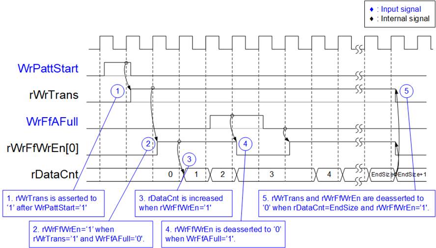
Figure 2‑6 Timing diagram of Write operation in TestGen
1) WrPattStart is asserted to �1� for one clock cycle when user sets the register to start write operation. In the next clock, rWrTrans is asserted to �1� to enable the control logic for generating write enable to FIFO.
2) Write enable to FIFO (rWrFfWrEn) is asserted to �1� when two conditions are met.
First, rWrTrans must be asserted to �1� during the write operation being active.
Second, the FIFO must not be full by monitoring WrFfAFull=�0�.
3) The write enable is also applied to be counter enable for counting total number of data (rDataCnt) in the write operation.
4) When FIFO is almost full (WrFfAFull=�1�), the write process is paused by de-asserting rWrFfWrEn to �0�.
5) When total data count is equal to the set value, rWrTrans is de-asserted to �0�. At the same time, rWrFfWrEn is also de-asserted to �0� to finish generating test data.
Comparing to write enable, the read enable signal is not stopped by total count and not started by start flag. When running read operation, read enable of FIFO is only controlled by empty flag of FIFO. When the read enable is asserted to �1�, the data counter and the address counter are increased for counting total data and generating the header of expect value respectively.
2.2 NVMeRAID0x4-IP
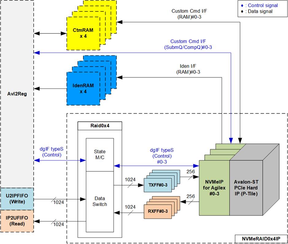
Figure 2‑7 NVMeRAID0x4 hardware
Figure 2‑7 shows the example to interface NVMeRAID0x4 in the reference design. The user interface of NVMeRAID0x4 consists of control interface and data interface. The control interface receives the command and the parameters from custom command interface or dgIF typeS, depending on the command. Custom command interface is used when operating SMART command or Flush command.
The data interface of NVMeRAID0x4 has four signal groups, i.e., FIFO input interface (dgIF typeS), FIFO output interface (dgIF typeS), custom command RAM interface, and Identify interface. Data bus width of FIFO interface is 1024-bit while the others are 256-bit. The custom command RAM interface is bi-directional interface while the others are unidirectional interface. In the reference design, the custom command RAM interface is used to transfer data of SMART command from NVMeRAID0x4 to Avl2Reg only. Another direction is not used.
2.2.1 NVMe-IP
NVMe-IP implements NVMe protocol of the host side to access one NVMe SSD directly without PCIe switch connection. NVMe-IP supports six commands, i.e., Write, Read, Identify, Shutdown, SMART, and Flush. NVMe-IP is designed to directly connect with PCIe hard IP (P-Tile). More details of the NVMe-IP are described in the datasheet.
https://dgway.com/products/IP/NVMe-IP/dg_nvme_datasheet_agl.pdf
2.2.2 Avalon-ST Intel Hard IP for PCIe (P-Tile)
This block is hard IP in Intel FPGA device which implements Physical, Data Link, and Transaction Layers of PCIe protocol. More details are described in Intel FPGA document.
https://www.intel.com/content/dam/www/programmable/us/en/pdfs/literature/ug/ug_ptile_pcie_avst.pdf
2.2.3 Two-port RAM
Two of two-Port RAMs, CtmRAM and IdenRAM, store data from Identify command and SMART command respectively. IdenRAM is simple dual-port RAM which has one read port and one write port. The data size of Identify command is 8 Kbytes, so IdenRAM size is 8Kbyte. NVMe-IP and Avl2Reg have different data bus size, so IdenRAM sets the different bus size for write port and read port. The data interface of NVMe-IP (write port) is 256-bit while the interface of Avl2Reg (read port) is 32-bit. Besides, NVMe-IP has double word enable to write only 32-bit data in some cases. The RAM setting on IP catalog of QuartusII supports the write byte enable. Therefore, one bit of double word enable is extended to be 4-bit write byte enable as shown in Figure 2‑8.
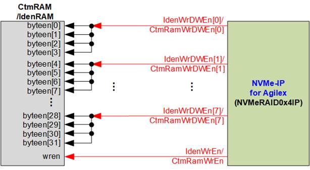
Figure 2‑8 Byte enable conversion logic
Bit[0], [1], �, [7] of WrDWEn are fed to bit[3:0], [7:4], �, [31:28] of IdenRAM byte write enable respectively.
Comparing with IdenRAM, CtmRAM is implemented by two-port RAM which has two write/read ports with byte enable. The connection to convert from word enable of NVMe-IP to byte enable of CtmRAM is similar to IdenRAM. Two-port RAM with two write/read ports is used to support the additional features when the customized custom command needs the data input. To support SMART command, using two-port RAM with one write/read port is enough. Though the data size returned from SMART command is 512 bytes, CtmRAM is implemented by 8Kbyte RAM for customized custom command.
2.2.4 FIFO
Two FIFOs are applied to interface one NVMe-IP with Raid0x4, TxFIFO and RxFIFO. Both FIFOs are asymmetric FIFO and has 64 Kbyte size. TxFIFO converts 1024-bit data (Raid0x4 data bus) to 256-bit data (NVMe-IP for Agilex data bus size) while RxFIFO converts 256-bit data to 1024-bit data.
2.2.5 Raid0x4
Raid0x4 consists of state machine and data switch for handling control interface and data interface respectively.
After receiving new command request from Avl2Reg, state machine calculates the address and transfer length of each NVMe-IP by decoding user parameter inputs. Next, state machine generates command request with the valid address and length to all NVMe-IPs. Also, state machine sets the active NVMe-IP channel to data switch for transferring data with the active channel.
The active NVMe-IP channel is selected by the current transferred address in 512-byte unit. When running with 4 NVMe-IPs, two lower bits (bit[1:0]) of the address are applied to select the active channel � �00�: NVMe-IP#0, �01�: NVMe-IP#1, �10�: NVMe-IP#2, and �11�: NVMe-IP#3. The current address is increased after finishing transferring 512-byte data which is stripe size of RAID0 system. Therefore, the active channel is switched to the next channel.
There are many pipeline registers inside data switch logic. Therefore, there is overhead time for switching the active channel before transferring 512-byte data. In the reference design, the overhead time is about 1 clock cycle while data is transferred for 4 clock cycles (4x1024-bit = 512 bytes). As a result, the overhead time is about 25% (1 cycle/4 cycles). To compensate the overhead time, clock frequency of Raid0x4 must be set to 25% higher than NVMe based clock. NVMe based clock for PCIe Gen4 that is run by 500 MHz is at least 250 MHz (500M/2). The clock frequency after compensating overhead time is 312.5 MHz (125% of 250 MHz). In the reference design, 350 MHz is applied to achieve the maximum performance for write and read command. As a result, write or read performance of Raid0x4 operation is almost equal to four times of one NVMe SSD performance.
The user Interface of Raid0x4 is shown in Table 2‑1. Control and data interface are designed to compatible to dgIF typeS format. Please see more details of dgIF typeS format from NVMe-IP datasheet.
Table 2‑1 Signal description of Raid0x4 (only User interface)
|
Signal |
Dir |
Description |
|
Control I/F of dgIF typeS |
||
|
RstB |
In |
Synchronous reset signal. Active low. De-assert to �1� when Clk signal is stable |
|
Clk |
In |
System clock for running Raid0x4 and NVMe-IP. It is recommended to use the frequency more than 312.5 MHz for PCIe Gen4 to achieve the best performance. The minimum requirement of Clk signal is the same as NVMe-IP (more than or equal to 250 MHz). |
|
UserCmd[2:0] |
In |
User Command (�000�: Identify, �001�: Shutdown, �010�: Write, �011�: Read, �100�: SMART, �110�: Flush, �101�/�111�: Reserved) |
|
UserAddr[47:0] |
In |
Start address to write or read Raid0x4 in 512-byte unit. It is recommended to set UserAddr[4:0]=00000b to align 16 Kbyte which is page size for four SSDs (one SSD page size is 4 Kbyte). Otherwise, write and read performance of some SSD models are reduced from 4Kbyte unaligned address. |
|
UserLen[47:0] |
In |
Total transfer size to write/read SSD in 512 byte unit. Valid from 1 to (LBASize-UserAddr). |
|
UserReq |
In |
Assert to �1� to send the new command request and de-assert to �0� after Raid0x4 starts the operation by asserting UserBusy to �1�. This signal can be asserted to �1� when Raid0x4 is Idle (UserBusy=�0�). Command parameter (UserCmd, UserAddr, UserLen, and CtmSubmDW0-DW15) must be valid and stable during UserReq=�1�. UserAddr and UserLen are inputs for Write/Read command while CtmSubmDW0-DW15 are inputs for SMART/Flush command. |
|
UserBusy |
Out |
Asserted to �1� when Raid0x5 is busy. New request must not be sent (UserReq to �1�) when Raid0x4 is busy (UserBusy=�1�). |
|
LBASize[47:0] |
Out |
Total capacity of four SSDs in 512-byte unit. This value is valid after finishing Identify command. It is recommended to run Identify command as the first command. Default value is 0. |
|
LBAMode |
Out |
LBA unit size of SSD. This signal is valid after finishing Identify command.. Default value is 0. �0�: LBA size = 512 byte, �1�: LBA size = 4 Kbyte. Raid0x4 uses 512-byte stripe size, so 4 Kbyte LBA size is not supported. |
|
UserError |
Out |
Error flag. Asserted to �1� when some bits of UserErrorType are not equal to 0. The flag can be cleared to �0� by asserting RstB to �0�. |
|
UserErrorType[0-3][31:0] |
Out |
Error status, directly mapped from UserErrorType in each NVMe-IP. [0]-IP#0, [1]-IP#1, [2]-IP#2, and [3]-IP#3 |
|
Data I/F of dgIF typeS |
||
|
UserFifoWrCnt[15:0] |
In |
Write data counter of Receive FIFO. Used to check full status of FIFO. When full status is detected, the returned data transmission from Read command may be paused. If the size of FIFO data count is less than 16-bit, please fill �1� to remained upper bit. |
|
UserFifoWrEn |
Out |
Asserted to �1� to write data to Receive FIFO during running Read command. |
|
UserFifoWrData[255:0] |
Out |
Write data bus of Receive FIFO. Valid when UserFifoWrEn=�1�. |
|
UserFifoRdCnt[15:0] |
In |
Read data counter of Transmit FIFO. Used to check data size stored in FIFO. The transmitted data packet for Write command may be paused when the counter shows empty status. If the size of FIFO data count is less than 16-bit, please fill �0� to remained upper bit. |
|
UserFifoEmpty |
In |
The signal is unused. |
|
UserFifoRdEn |
Out |
Asserted to �1� to read data from Transmit FIFO during running Write command. |
|
UserFifoRdData[255:0] |
In |
Read data returned from Transmit FIFO. Valid in the next clock after UserFifoRdEn is asserted to �1�. |
Timing diagram of Raid0x4 module when running Write command is shown as follows.
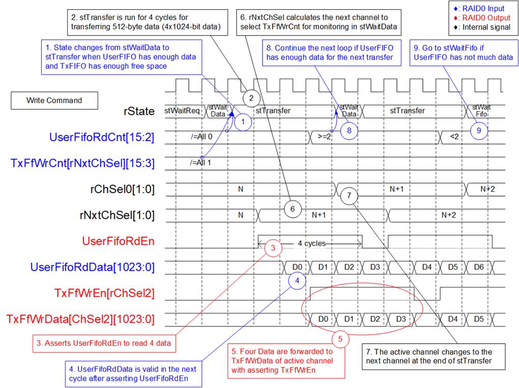
Figure 2‑9 Raid0x4 timing diagram in Write command
When user sends Write command to Raid0x4, data is forwarded from UserFIFO (U2IPFIFO) to TxFIFO[0]-[3]. One TxFIFO is active to transfer 512-byte data at a time. After that, the active NVMe channel is switched to the next channel for transferring data, following RAID0 behavior.
(1) stWaitData is the core state of Raid0x4 module. First, it checks the remained transfer size. The operation is finished when the remained transfer size is equal to 0. Otherwise, UserFifoRdCnt and TxFfWrCnt are monitored to confirm that at least 512-byte data is stored in U2IPFIFO and TxFIFO has at least 1024-byte free space. If FIFOs are ready, the write operation is started.
Note:
1) TxFfWrCnt of four channels are fed to multiplexer to select the active channel. Therefore, it has one clock latency, comparing to UserFifoRdCnt.
ii) TxFfWrCnt is controlled by rNxtChSel which is the active channel in the next �stTransfer� running. After starting the first transfer loop, rNxtChSel is increased for scanning free space size of the next active channel FIFO.
(2) State machines changes to stTransfer to start forwarding the write data from user logic to TxFIFO.
(3) UserFifoRdEn is asserted to �1� for 4 clock cycles to read 512-byte data from UserFIFO.
(4) When using standard FIFO, Read data (UserFifoRdData) is valid in the next cycle after asserting Read enable (UserFifoRdEn).
(5) The data is forwarded to TxFIFO of the active channel, selected by rChSel2 which is two-clock latency signal of rChSel0.
Note: rChSel0 shows the active channel for transferring data in stTransfer state.
(6) When running in stTransfer state, rNxtChSel calculates the next active channel from rChSel0. rNxtChSel is applied to select the active channel for reading TxFfWrCnt which is read in stWaitData.
(7) The active channel for transferring data (rChSel0) is increased after finishing 512-byte data transferring in stTransfer state.
(8) To reduce overhead time for running the next transfer loop, UserFifoRdCnt is monitored in stTransfer state. If read counter shows at least 2x512-byte data is stored in FIFO, the new transfer loop will be started in the next cycle by changing to stWaitData and returning to step 1. Otherwise, the next state is stWaitFifo, described in step 9.
(9) stWaitFIFO is designed to wait until the current data transferring is completed and UserFifoRdCnt is valid for monitoring. After waiting for three clock cycles, the state changes to stWaitData to continue the next transfer or complete the operation.
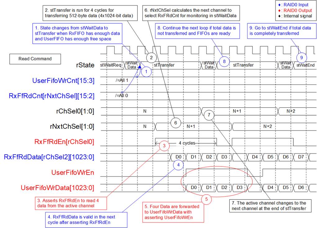
Figure 2‑10 Raid0x4 timing diagram in Read command
When user sends Read command to RAID0, data is forwarded from RxFIFO[0]-[3] to IP2UFIFO. Similar to Write command, one RxFIFO is active to transfer 512-byte at a time. The active channel is switched to the next channel after finishing transferring 512-byte data, following RAID0 behavior.
(1) stWaitData is the state to check the remained transfer length and FIFO status. In read command, RxFfRdCnt and UserFifoWrCnt are monitored to confirm that at least 512-byte data is stored in RxFIFO and IP2UFIFO has at least 1024-byte free space. The read operation is started when both FIFO status are ready and there is remained transfer length.
Note:
i. RxFfRdCnt of four channels are fed to multiplexer to select the active channel. Therefore, it has one clock latency, comparing to UserFifoWrCnt.
ii. RxFfRdCnt is controlled by rNxtChSel which is the active channel in the next stTransfer running.
(2) State machines changes to stTransfer to start forwarding the read data from RxFIFO to user logic.
(3) RxFfRdEn of the active channel, selected by rChSel0, is asserted to �1� for 4 clock cycles to read 512-byte data from RxFIFO.
(4) When using standard FIFO, Read data (RxFfRdData) is valid in the next cycle after asserting Read enable (RxFfRdEn).
(5) The data of the active channel, selected by rChSel2, is forwarded to UserFIFO.
Note: rChSel2 is ChSel0 signal with two-clock latency.
(6) When running in stTransfer state, rNxtChSel calculates the next active channel from rChSel0. rNxtChSel is applied to select the active channel for reading RxFfRdCnt which is monitored in stWaitData.
(7) The active channel for transferring data (rChSel0) is increased after finishing 512-byte data transferring in stTransfer state.
(8) If there is remained transfer length, the state changes to stTransfer to start new data transferring, similar to step 2. Otherwise, the next state is stWaitEnd, described in step 9.
(9) If all data are completely transferred, the state changes to stWaitEnd to wait until all devices finishes operation by de-asserting Busy signal to �0�.
2.3 CPU and Peripherals
32-bit Avalon-MM bus is applied to be the bus interface for CPU accessing the peripherals such as Timer and JTAG UART. CPU assigns the different base address and the address range to each peripheral for accessing one peripheral at a time. The test system of NVMe-IP is connected with CPU as a peripheral on 32-bit Avalon-MM bus for CPU controlling and monitoring
In the reference design, Avl2Reg module is designed to connect the CPU system via Avalon-MM bus standard. CPU specifies the base address and the range to write/read access with Avl2Reg. More details of Avl2Reg are shown in Figure 2‑11.
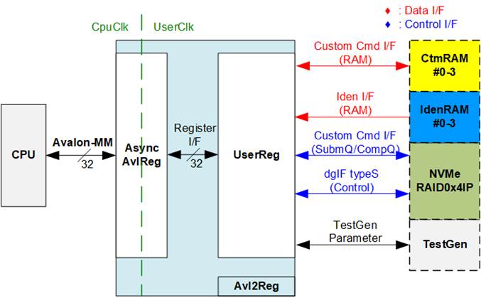
Figure 2‑11 CPU and peripherals hardware
Avl2Reg consists of AsyncAvlReg and UserReg. AsyncAvlReg is designed to convert the Avalon-MM signals to be the simple register interface which has 32-bit data bus size, similar to Avalon-MM data bus size. In addition, AsyncAvlReg includes asynchronous logic to support clock domain crossing between CpuClk domain and UserClk domain.
UserReg includes the register file for setting the parameters and storing the status signals of other modules in the test system, i.e., CtmRAM, IdenRAM, NVMeRAID0x4, and TestGen. More details of AsyncAvlReg and UserReg are described as follows.
2.3.1 AsyncAvlReg
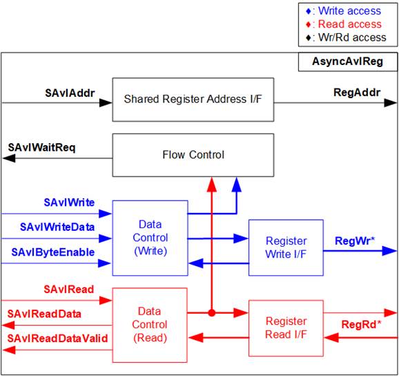
Figure 2‑12 AsyncAxiReg Interface
The signal on Avalon-MM bus interface can be split into three groups, i.e., Write channel (blue color), Read channel (red color), and Shared control channel (black color). More details of Avalon-MM interface specification are described in following document.
https://www.intel.com/content/dam/www/programmable/us/en/pdfs/literature/manual/mnl_av alon_spec.pdf
According to Avalon-MM specification, one command (write or read) can be operated at a time. The logics inside AsyncAvlReg are split into three groups, i.e., Write control logic, Read control logic, and Flow control logic. Flow control logic controls SAvlWaitReq to hold the next request from Avalon-MM interface if the current request does not finish. Write control and Write data I/F of Avalon-MM bus are latched and transferred to be Write register interface with clock domain crossing registers. Similarly, Read control I/F are latched and transferred to be Read register interface with clock domain crossing registers. After that, the returned data from Register Read I/F is transferred to Avalon-MM bus by using clock domain crossing registers. Address I/F of Avalon-MM is latched and transferred to Address register interface as well.
The simple register interface is compatible with single-port RAM interface for write transaction. The read transaction of the register interface is slightly modified from RAM interface by adding RdReq and RdValid signals for controlling read latency time. The address of register interface is shared for write and read transaction, so user cannot write and read the register at the same time. The timing diagram of the register interface is shown in Figure 2‑13.
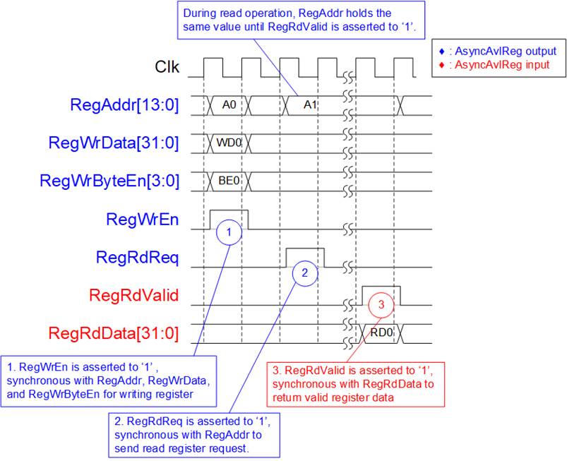
Figure 2‑13 Register interface timing diagram
1) To write register, the timing diagram is similar to single-port RAM interface. RegWrEn is asserted to �1� with the valid signal of RegAddr (Register address in 32-bit unit), RegWrData (write data of the register), and RegWrByteEn (the write byte enable). Byte enable has four bits to be the byte data valid. Bit[0], [1], [2], and [3] are equal to �1� when RegWrData[7:0], [15:8], [23:16], and [31:24] are valid respectively
2) To read register, AsyncAvlReg asserts RegRdReq to �1� with the valid value of RegAddr. 32-bit data is returned after receiving the read request. The slave detects RegRdReq signal and starts the read transaction. During read operation, the address value (RegAddr) does not change until RegRdValid is asserted to �1�. Therefore, the address can be used for selecting the returned data by using multiple layers of multiplexer.
3) The read data is returned on RegRdData bus by the slave with asserting RegRdValid to �1�. After that, AsyncAvlReg forwards the read value to SAvlRead interface.
2.3.2 UserReg
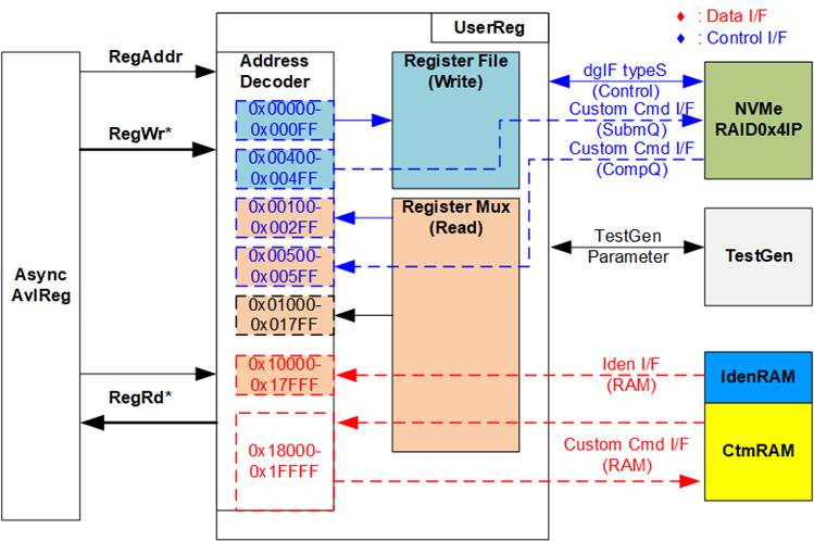
Figure 2‑14 UserReg Interface
UserReg consists of many registers for interfacing with other modules. The address for write or read access is decoded by Address decoder to select the active register. There are seven regions mapping in UserReg, described as follows.
1) 0x00000 � 0x000FF : mapped to set the test parameters of NVMeRAID0x4 and TestGen. This area is write-access only.
2) 0x00100 � 0x002FF : mapped to read the status of NVMeRAID0x4. This area is read-access only.
3) 0x00400 � 0x004FF : mapped to set the test parameters of custom command interface. This area is write-access only.
4) 0x00500 � 0x005FF : mapped to read the status of custom command interface. This area is read-access only.
5) 0x01000 � 0x017FF : mapped to read the status of TestGen. This area is read-access only.
6) 0x10000 � 0x17FFF : mapped to read data from IdenRAM. This area is read-access only.
7) 0x18000 � 0x1FFFF : mapped to custom command RAM interface. Although this area supports both write and read access, the demo shows only read access by running SMART command.
Address decoder decodes the upper bit of RegAddr for selecting the active hardware. The register file inside UserReg is 32-bit bus size. Write byte enable (RegWrByteEn) is not applied in the test system because the CPU uses 32-bit pointer to set the hardware register.
To read register, three-step multiplexer is designed to select the read data within each address area. The lower bit of RegAddr is applied in each Register area to select active data. Next, the address decoder uses the upper bit to select the read data from active area and returns to CPU. Totally, the latency of read data is equal to three clock cycles. Therefore, RegRdValid is created by RegRdReq with asserting three D Flip-flops. More details of the address mapping within UserReg module are shown in Table 2‑2.
Table 2‑2 Register Map
|
Address |
Register Name |
Description |
|
Wr/Rd |
(Label in �nvmeraid0g4test.c�) |
|
|
0x00000 � 0x000FF: Control signals of NVMeRAID0x4 and TestGen (Write access only) |
||
|
BA+0x00000 |
User Address (Low) Reg |
[31:0]: Input to be bit[31:0] of start address in 512-byte unit (UserAddr[31:0] of dgIF typeS for RAID0) |
|
(USRADRL_REG) |
||
|
BA+0x00004 |
User Address (High) Reg |
[15:0]: Input to be bit[47:32] of start address in 512-byte unit (UserAddr[47:32] of dgIF typeS for RAID0) |
|
(USRADRH_REG) |
||
|
BA+0x00008 |
User Length (Low) Reg |
[31:0]: Input to be bit[31:0] of transfer length in 512-byte unit (UserLen[31:0] of dgIF typeS for RAID0) |
|
(USRLENL_REG) |
||
|
BA+0x0000C |
User Length (High) Reg |
[15:0]: Input to be bit[47:32] of transfer length in 512-byte unit (UserLen[47:32] of dgIF typeS for RAID0) |
|
(USRLENH_REG) |
||
|
BA+0x00010 |
User Command Reg |
[2:0]: Input to be user command (UserCmd of dgIF typeS for RAID0) �000�: Identify, �001�: Shutdown, �010�: Write RAID, �011�: Read RAID, �100�: SMART, �110�: Flush, �101�/�111�: Reserved. When this register is written, the command request is sent to RAID0. After that, the IP starts operating the command. |
|
(USRCMD_REG) |
||
|
BA+0x00014 |
Test Pattern Reg |
[2:0]: Select test pattern �000�-Increment, �001�-Decrement, �010�-All 0, �011�-All 1, �100�-LFSR |
|
(PATTSEL_REG) |
||
|
BA+0x00020 |
NVMe Timeout Reg |
[31:0]: Input to be timeout value of all NVMe-Ips (TimeOutSet[31:0] of NVMe-IP) |
|
(NVMTIMEOUT_REG) |
||
|
0x00100 � 0x002FF: Status signals of NVMeRAID0x4 (Read access only) |
||
|
BA+0x0100 |
User Status Reg |
[0]: UserBusy of dgIF typeS for RAID0 (�0�: Idle, �1�: Busy) [1]: UserError of dgIF typeS for RAID0 (�0�: Normal, �1�: Error) [2]: Data verification fail (�0�: Normal, �1�: Error) |
|
(USRSTS_REG) |
||
|
BA+0x0104 |
Total device size (Low) Reg |
[31:0]: Mapped to LBASize[31:0] of RAID0 to show RAID0 capacity |
|
(LBASIZEL_REG) |
||
|
BA+0x0108 |
Total device size (High) Reg |
[15:0]: Mapped to LBASize[47:32] of RAID0 [31]: Mapped to LBAMode of RAID0 |
|
(LBASIZEH_REG) |
||
|
(BA+0x0110)- (BA+0x011F) |
User Error Type CH#0-#3 Reg |
0x0110: NVMe-IP#0, 0x0114: NVMe-IP#1, 0x0118: NVMe-IP#2, 0x011C: NVMe-IP#3 [31:0]: Mapped to UserErrorType of NVMe-IP |
|
(USRERRTYPE0-3_REG) |
||
|
(BA+0x0120)- (BA+0x012F) |
PCIe Status CH#0-#3 Reg |
0x0120: NVMe-IP#0, 0x0124: NVMe-IP#1, 0x0128: NVMe-IP#2, 0x012C: NVMe-IP#3 [0]: PCIe linkup status (�0�: No linkup, �1�: linkup) [3:2]: Two lower bits to show PCIe link speed. MSB is bit[16]. (�000�: Not linkup, �001�: PCIe Gen1, �010�: PCIe Gen2, �011�: PCIe Gen3, �111�: PCIe Gen4) [6:4]: PCIe link width status (�001�: 1-lane, �010�: 2-lane, �100�: 4-lane) [13:8]: Current LTSSM State of PCIe hard IP. Please see more details of LTSSM value in PCIe hard IP datasheet [16]: The upper-bit to show PCIe link speed of PCIe hard IP. Two lower bits are bit[3:2]. |
|
(PCIESTS0-3_REG) |
||
|
(BA+0x0130)- (BA+0x013F) |
Completion Status CH#0-#3 Reg |
0x0130: NVMe-IP#0, 0x0134: NVMe-IP#1, 0x0138: NVMe-IP#2, 0x013C: NVMe-IP#3 [15:0]: Status from Admin completion (AdmCompStatus[15:0] of NVMe-IP) [31:16]: Status from I/O completion (IOCompStatus[15:0] of NVMe-IP) |
|
(COMPSTS0-3_REG) |
||
|
(BA+0x0140)- (BA+0x014F) |
NVMe CAP CH#0-#3 Reg |
0x0140: NVMe-IP#0, 0x0144: NVMe-IP#1, 0x0148: NVMe-IP#2, 0x014C: NVMe-IP#3 [31:0]: Mapped to NVMeCAPReg of NVMe-IP |
|
(NVMCAP0-3_REG) |
||
|
(BA+0x00150)- (BA+0x0015F) |
NVMe IP Test pin CH#0-#3 Reg |
0x0150: NVMe-IP#0, 0x0154: NVMe-IP#1, 0x0158: NVMe-IP#2, 0x015C: NVMe-IP#3 [31:0]: TestPin output from NVMe-IP. |
|
(NVMTESTPIN0-3_REG) |
||
|
Address |
Register Name |
Description |
|
Wr/Rd |
(Label in �nvmeraid0g4test.c�) |
|
|
0x00400 � 0x005FF: Custom command of NVMeRAID0x4 |
||
|
(BA+0x00400)- (BA+0x004FF) |
Custom Submission Queue CH#0�#3 Reg |
[31:0]: Submission queue entry of SMART and Flush command. Input to be CtmSubmDW0-DW15 of NVMe-IP#0-#3 successively. 0x400: DW0, 0x404: DW1, �, 0x43C: DW15 of NVMe-IP#0 0x440: DW0, 0x444: DW1, �, 0x47C: DW15 of NVMe-IP#1 0x480: DW0, 0x484: DW1, �, 0x4BC: DW15 of NVMe-IP#2 0x4C0: DW0, 0x4C4: DW1, �, 0x4FC: DW15 of NVMe-IP#3 |
|
Wr |
(CTMSUBMQ0-3_REG) |
|
|
(BA+0x00500)- (BA+0x0053F) |
Custom Completion Queue CH#0�#3 Reg |
[31:0]: CtmCompDW0-DW3 output from NVMe-IP#0-#3 successively. 0x500: DW0, 0x504: DW1, �, 0x50C: DW3 of NVMe-IP#0 0x510: DW0, 0x514: DW1, �, 0x51C: DW3 of NVMe-IP#1 0x520: DW0, 0x524: DW1, �, 0x52C: DW3 of NVMe-IP#2 0x530: DW0, 0x534: DW1, �, 0x53C: DW3 of NVMe-IP#3 |
|
Rd |
(CTMCOMPQ0-3_REG) |
|
|
BA+0x00800 |
IP Version Reg |
[31:0]: IP version number (IPVersion[31:0] of NVMe-IP) |
|
Rd |
(IPVERSION_REG) |
|
|
0x01000 � 0x017FF: Status signals of TestGen (Read access only) |
||
|
BA+0x01000 |
Data Failure Address(Low) Reg |
[31:0]: Bit[31:0] of the byte address of the 1st failure position in Read command |
|
(RDFAILNOL_REG) |
||
|
BA+0x01004 |
Data Failure Address(High) Reg |
[24:0]: Bit[56:32] of the byte address of the 1st failure position in Read command |
|
(RDFAILNOH_REG) |
||
|
BA+0x01008 |
Current test byte (Low) Reg |
[31:0]: Bit[31:0] of the current test data size in TestGen module |
|
(CURTESTSIZEL_REG) |
||
|
BA+0x0100C |
Current test byte (High) Reg |
[24:0]: Bit[56:32] of the current test data size in TestGen module |
|
(CURTESTSIZEH_REG) |
||
|
(BA+0x01200)- (BA+0x0127C) |
Expected value Word0-31 Reg |
0x1200: Bit[31:0], 0x1204: Bit[63:32], �, 0x127C: Bit[1023:992] of the expected data at the 1st failure position in Read command. |
|
(EXPPATW0-W31_REG) |
||
|
(BA+0x01400)- (BA+0x0147C) |
Read value Word0-31 Reg |
0x1400: Bit[31:0], 0x1404: Bit[63:32], �, 0x147C: Bit[1023:992] of the read data at the 1st failure position in Read command. |
|
(RDPATW0-W31_REG) |
||
|
0x10000 � 0x1FFFF: Identify RAM and Custom RAM |
||
|
(BA+0x10000) � (BA+0x17FFF) |
Identify Controller Data CH#0-#3 |
0x10000-0x10FFF: 4Kbyte Identify controller data of NVMe-IP#0 0x11000-0x11FFF: 4Kbyte Identify namespace data of NVMe-IP#0 0x12000-0x12FFF: 4Kbyte Identify controller data of NVMe-IP#1 0x13000-0x13FFF: 4Kbyte Identify namespace data of NVMe-IP#1 0x14000-0x14FFF: 4Kbyte Identify controller data of NVMe-IP#2 0x15000-0x15FFF: 4Kbyte Identify namespace data of NVMe-IP#2 0x16000-0x16FFF: 4Kbyte Identify controller data of NVMe-IP#3 0x17000-0x17FFF: 4Kbyte Identify namespace data of NVMe-IP#3 |
|
Rd |
(IDENCTRL0-3_REG/ IDENNAME0-3_REG) |
|
|
(BA+0x18000) � (BA+0x1FFFF) |
Custom command Ram CH#0-#3
|
0x18000-0x19FFF: NVMe-IP#0, 0x1A000-0x1BFFF: NVMe-IP#1, 0x1C000-0x1DFFF: NVMe-IP#2, 0x1E000-0x1FFFF: NVMe-IP#3 8K byte CtmRAM interface of NVMe-IP#0-#3. Used to store 512-byte data output from SMART Command |
|
Wr/Rd |
(CTMRAM0-3_REG) |
|
3 CPU Firmware
3.1 Test firmware (nvmeraid0g4test.c)
After system boot-up, CPU runs following steps to finish the initialization process.
1) CPU initializes its peripherals such as JTAG UART and Timer.
2) CPU waits until PCIe connection links up (PCIESTS0-3_REG[0]= �1�).
3) CPU waits until NVMeRAID0x4 completes initialization process (USRSTS_REG[0]=�0�). The error message is displayed and the process stops when some errors are found.
4) CPU displays PCIe link status (the number of PCIe lanes and the PCIe speed) by reading PCIESTS0-3_REG[16:2].
5) CPU displays the main menu. There are six menus for running six commands with RAID0, i.e., Identify, Write, Read, SMART, Flush, and Shutdown.
More details of each command are described as follows.
3.1.1 Identify command
The step to operate Identify command is described as follows.
1) Set USRCMD_REG[2:0]=�000�. Next, Test logic generates command and asserts command request to NVMeRAID0x4. After that, busy flag (USRSTS_REG[0]) changes from �0� to �1�.
2) CPU waits until the operation is completed or some errors are found by monitoring USRSTS_REG[1:0].
Bit[0] is de-asserted to �0� when command is completed. After that, the data from Identify command is stored to IdenRAM.
Bit[1] is asserted to �1� when some errors are detected. The error message is displayed on the console to show the error details (read from USRERRTYPE0-3_REG[31:0]). Finally, the process is stopped.
3) After busy flag (USRSTS_REG[0]) is de-asserted to �0�, CPU decodes SSD model name from IdenRAM (IDENCTRL0-3_REG) and reads RAID0 capacity (LBASIZEL/H_REG) from NVMeRAID0x4 output to display on the console. Finally, CPU checks LBA mode of RAID0 (LBASIZEH_REG[31]). If LBA Size of RAID0 is 4Kbyte which is not supported by RAID0 controller, the process is stopped and the error message is displayed.
3.1.2 Write/Read command
The step to operate Write/Read command is described as follows.
1) Receive start address, transfer length, and test pattern from JTAG UART. When some inputs are invalid, the operation is cancelled.
2) Get all inputs and set to USRADRL/H_REG, USRLENL/H_REG, and PATTSEL_REG.
3) Set USRCMD_REG[2:0]=�010� for Write command or �011� for Read command. After that, the new command request is sent to NVMeRAID0x4 for running Write or Read command. Busy flag (USRSTS_REG[0]) changes from �0� to �1�.
4) CPU waits until the operation is completed or some errors (except verification error) are found by monitoring USRSTS_REG[2:0].
Bit[0] is de-asserted to �0� when command is completed.
Bit[1] is asserted to �1� when some errors are detected. The error message is displayed on the console to show the error details, decoded from USRERRTYPE0-3_REG[31:0] and the process is stopped.
Bit[2] is asserted to �1� when data verification is failed. The verification error message is displayed on the console to show the error details. In this condition, CPU is still run until the operation is done or user presses any key(s) to cancel operation.
During running the operation, current transfer size read from CURTESTSIZEL/H_REG is displayed every second.
5) After busy flag (USRSTS_REG[0]) is de-asserted to �0�, CPU calculates and displays the test result on the console, i.e., total time usage, total transfer size, and transfer speed.
3.1.3 SMART Command,
The step to operate SMART command is described as follows.
1) Set 16-Dword of Submission queue entry (CTMSUBMQ0-3_REG) to be SMART command value.
2) Set USRCMD_REG[2:0]=�100�. Next, Test logic generates command and asserts the request to NVMeRAID0x4. After that, busy flag (USRSTS_REG[0]) changes from �0� to �1�.
3) CPU waits until the operation is completed or some errors are found by monitoring USRSTS_REG[1:0].
Bit[0] is de-asserted to �0� when command is completed. After that, the data returned from SMART command is stored to CtmRAM.
Bit[1] is asserted to �1� when some errors are detected. The error message is displayed on the console to show the error details, decoded from USRERRTYPE0-3_REG[31:0]. Finally, the process is stopped.
4) After busy flag (USRSTS_REG[0]) is de-asserted to �0�, CPU decodes SMART command information from CtmRAM (CTMRAM0-3_REG), i.e., Remaining Life, Percentage Used, Temperature, Total Data Read, Total Data Written, Power On Cycles, Power On Hours, and Number of Unsafe Shutdown.
More details of SMART log are described in NVM Express Specification.
https://nvmexpress.org/resources/specifications/
3.1.4 Flush Command
The step to operate Flush command is described as follows.
1) Set 16-Dword of Submission queue entry (CTMSUBMQ0-3_REG) to be Flush command value.
2) Set USRCMD_REG[2:0]=�110�. Next, Test logic generates command and asserts the request to NVMeRAID0x4. After that, busy flag (USRSTS_REG[0]) changes from �0� to �1�.
3) CPU waits until the operation is completed or some errors are found by monitoring USRSTS_REG[1:0].
Bit[0] is de-asserted to �0� when command is completed. After that, CPU goes back to the main menu.
Bit[1] is asserted to �1� when some errors are detected. The error message is displayed on the console to show the error details, decoded from USRERRTYPE0-3_REG[31:0]. Finally, the process is stopped.
3.1.5 Shutdown Command
The step to operate Shutdown command is described as follows.
1) Set USRCMD_REG[2:0]=�001�. Next, Test logic generates command and asserts the request to NVMeRAID0x4. After that, busy flag (USRSTS_REG[0]) changes from �0� to �1�.
2) CPU waits until the operation is completed or some errors are found by monitoring USRSTS_REG[1:0].
Bit[0] is de-asserted to �0� when command is completed. After that, the CPU goes to the next step.
Bit[1] is asserted to �1� when some errors are detected. The error message is displayed on the console to show the error details, decoded from USRERRTYPE0-3_REG[31:0]. Finally, the process is stopped.
3) After busy flag (USRSTS_REG[0]) is de-asserted to �0�, all SSDs and all NVMe-IPs change to inactive status. The CPU cannot receive the new command from user. The user must power off the test system.
3.2 Function list in Test firmware
|
int exec_ctm(unsigned int user_cmd) |
|
|
Parameters |
user_cmd: 4-SMART command, 6-Flush command |
|
Return value |
0: No error, -1: Some errors are found in NVMeRAID0x4 |
|
Description |
Run SMART command or Flush command, following in topic 3.1.3 (SMART Command,) and 3.1.4 (Flush Command). |
|
unsigned long long get_cursize(void) |
|
|
Parameters |
None |
|
Return value |
Read value of CURTESTSIZEH/L_REG |
|
Description |
Read CURTESTSIZEH/L_REG and return read value as function result. |
|
int get_param(userin_struct* userin) |
|
|
Parameters |
userin: Three inputs from user, i.e., start address, total length in 512-byte unit, and test pattern |
|
Return value |
0: Valid input, -1: Invalid input |
|
Description |
Receive the input parameters from the user and verify the value. When the input is invalid, the function returns -1. Otherwise, all inputs are updated to userin parameter. |
|
void iden_dev(void) |
|
|
Parameters |
None |
|
Return value |
None |
|
Description |
Run Identify command, following in topic 3.1.1 (Identify command). |
|
int setctm_flush(void) |
|
|
Parameters |
None |
|
Return value |
0: No error, -1: Some errors are found in NVMeRAID0x4 |
|
Description |
Set Flush command to CTMSUBMQ0-3_REG and call exec_ctm function to start Flush command. |
|
int setctm_smart(void) |
|
|
Parameters |
None |
|
Return value |
0: No error, -1: Some errors are found in NVMeRAID0x4 |
|
Description |
Set SMART command to CTMSUBMQ0-3_REG and call exec_ctm function to start SMART command. Finally, decode and display SMART information on the console |
|
void show_error(void) |
|
|
Parameters |
None |
|
Return value |
None |
|
Description |
Read USRERRTYPE0-3_REG, decode the error flag, and display error message following the error flag of each channel. |
|
void show_pciestat(void) |
|
|
Parameters |
None |
|
Return value |
None |
|
Description |
Read PCIESTS0-3_REG until the read value from two read times is stable. After that, display the read value on the console. |
|
void show_result(void) |
|
|
Parameters |
None |
|
Return value |
None |
|
Description |
Print total size by calling get_cursize and show_size function. After that, calculate total time usage from global parameters (timer_val and timer_upper_val) and display in usec, msec, or sec unit. Finally, transfer performance is calculated and displayed in MB/s unit. |
|
void show_size(unsigned long long size_input) |
|
|
Parameters |
size_input: Transfer size to display on the console |
|
Return value |
None |
|
Description |
Calculate and display the input value in Mbyte, Gbyte, or Tbyte unit |
|
void show_smart_hex(unsigned char *char_ptr16B) |
|
|
Parameters |
*char_ptr16B |
|
Return value |
None |
|
Description |
Display SMART data as hexadecimal unit. |
|
void show_smart_raw(unsigned char *char_ptr16B) |
|
|
Parameters |
*char_ptr16B |
|
Return value |
None |
|
Description |
Display SMART data as decimal unit when the input value is less than 4 MB. Otherwise, display overflow message. |
|
void show_smart_unit(unsigned char *char_ptr16B) |
|
|
Parameters |
*char_ptr16B |
|
Return value |
None |
|
Description |
Display SMART data as GB or TB unit. When the input value is more than limit (500 PB), the overflow message is displayed instead. |
|
void show_vererr(void) |
|
|
Parameters |
None |
|
Return value |
None |
|
Description |
Read RDFAILNOL/H_REG (error byte address), EXPPATW0-W31_REG (expected value), and RDPATW0-W31_REG (read value) to display verification error details on the console. |
|
void shutdown_dev(void) |
|
|
Parameters |
None |
|
Return value |
None |
|
Description |
Run Shutdown command, following in topic 3.1.5 (Shutdown Command) |
|
int wrrd_dev(unsigned int user_cmd) |
|
|
Parameters |
user_cmd: 2-Write command, 3-Read command |
|
Return value |
0: No error, -1: Receive invalid input or some errors are found. |
|
Description |
Run Write command or Read command, following in topic 3.1.2 (Write/Read command) |
4 Example Test Result
The example test result when running RAID0 demo system by four NVMe Gen4 SSD (1 TB WD Black SN850) is displayed in Figure 4‑1.
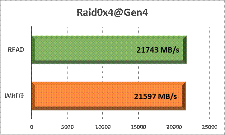
Figure 4‑1 Performance of 4-ch RAID0 demo by using 4 SSDs Gen4
When running 4-ch RAID0 with 4 SSDs@Gen4 speed, write performance and read performance are about 21,000 Mbyte/sec.
Note: By using default IP that uses 256 Kbyte memory, the read performance of some SSDs is slower than the NVMe-IP that uses 1 Mbyte memory. Please contact our sales for the system that is sensitive to Read performance.
5 Revision History
|
Revision |
Date |
Description |
|
1.0 |
23-Jun-21 |
Initial version release |
|
1.1 |
9-Sep-21 |
Update Test result when using same SSDs |
Copyright: 2021 Design Gateway Co,Ltd.