Rev1.2 3-Jul-23
1 Overview
This document describes the instruction to run NVMe-IP with DDR demo on FPGA development board. The demo is designed to test Write or Read command with one NVMe SSD as sustain rate. The user can set DDR size usage for transferring the data as sustain rate to check the minimum memory size requirement to run the SSD. Also, the other commands that are supported by NVMe-IP can be run in the demo - Identify, SMART, Flush, and Shutdown command. User controls test operation via FGPA console.
After user finishes FPGA board setup following “dg_nvmeip_fpgasetup” document, main menu is displayed and then user can set the input to the console for selecting the test operation.
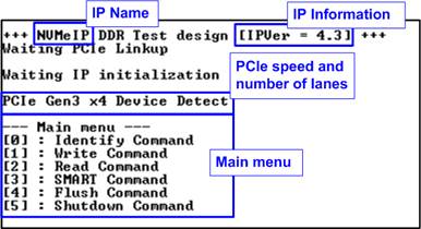
Figure 1‑1 NVMe-IP with DDR main menu
On welcome screen, IP name and IP version number are displayed. The PCIe speed and number of PCIe lanes are displayed in the next message. Finally, the test menu is displayed on the console.
2 Test Menu
2.1 Identify Command
Select ‘0’ to send Identify command to NVMe SSD.
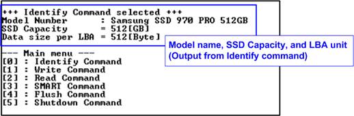
Figure 2‑1 Test result when running Identify command
After finishing the operation, the SSD information output from Identify command is displayed. The console shows three values.
1) SSD model number: This value is decoded from Identify controller data.
2) SSD capacity: This value is signal output from NVMe-IP.
3) Data size per LBA: This value is signal output from NVMe-IP. Two values are supported – 512-byte and 4-Kbyte.
2.2 Write Command
Select ‘1’ to send Write command to NVMe SSD.
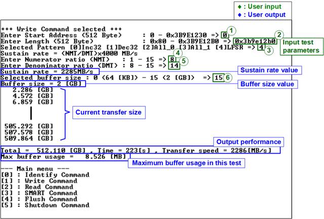
Figure 2‑2 Test result when running Write command
User inputs six parameters as follows.
1) Start Address: Input start address to write SSD as 512-byte unit. The input is decimal unit when user enters only digit number. User can add “0x” to be prefix for hexadecimal unit. When LBA unit of SSD is 4 Kbyte, this input must be aligned to 8.
2) Transfer Length: Input total transfer size as 512-byte unit. The input is decimal unit when user enters only digit number. User can add “0x” to be prefix for hexadecimal unit. When LBA unit of SSD is 4 Kbyte, this input must be aligned to 8.
3) Test pattern: Select test data pattern for writing to SSD. There are five patterns, i.e., 32-bit incremental, 32-bit decremental, all 0, all 1, and 32-bit LFSR counter.
4) Numerator ratio (NMT): Input numerator of transfer rate ratio. Valid value is 1 to 15.
5) Denominator ratio (DMT): Input denominator of transfer rate ratio. Valid value is NMT input to 15. The equation to set the transfer rate is as follows.
Transfer rate (MB/s) = (NMT/DMT) x 4000 (250 MHz x 128-bit)
Note: 4000 is the test data performance in the hardware which uses 250 MHz for transferring 128-bit data. Therefore, the maximum rate is 250 MHz x 128-bit = 4000 MB/s.
Thus, when NMT=8 and DMT=14, the transfer rate is 8/14 x 4000 = 2285 MB/s.
6) Buffer size: Input buffer size to use in this transfer. Valid value is 0-15. The details to set the buffer size is shown as below.
Table 2‑1 Buffer size setting
|
Set value |
Buffer size |
|
0 |
64 KB |
|
1 |
128 KB |
|
2 |
256 KB |
|
3 |
512 KB |
|
4 |
1 MB |
|
5 |
2 MB |
|
6 |
4 MB |
|
7 |
8 MB |
|
8 |
16 MB |
|
9 |
32 MB |
|
10 |
64 MB |
|
11 |
128 MB |
|
12 |
256 MB |
|
13 |
512 MB |
|
14 |
1 GB |
|
15 |
2 GB |
Note: KB-1024 bytes, MB-1024x1024 bytes, and GB-1024x1024x1024 bytes
When all inputs are valid, the operation begins. While writing data, current transfer size is displayed on the console every second to show the progress of the test. Finally, total size, total time usage, test speed, and maximum buffer usage are displayed on the console as test result.
As shown in Figure 2‑2, writing data at 2285 MB/s with full disk size can be done without error when setting 2-GByte buffer size. However, the result shows the maximum buffer usage while running the test is about 8.526 MB. Thus, it is expected that the user can re-run the test by reducing the buffer size to 16 MB (Set value=8) and the test should be run successfully.
Typically, the buffer size usage is reduced when the transfer speed is reduced. Also, it depends on SSD characteristic. Most enterprise SSDs show more stable performance than the consumer SSDs.
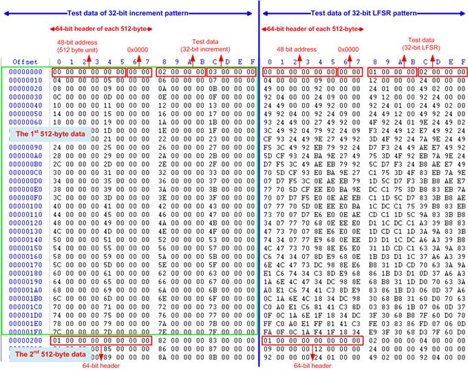
Figure 2‑3 Example Test data of the 1st and 2nd 512-byte by using incremental/LFSR pattern
Test data in SSD is split into 512-byte unit. For incremental, decremental, and LFSR pattern, each 512-byte data has unique 64-bit header consisting of 48-bit address (in 512-byte unit) and 16-bit zero value. The data after 64-bit header is the test pattern which is selected by user.
The left window of Figure 1-3 shows the example when using 32-bit incremental pattern while the right window shows the example when using 32-bit LFSR pattern. The unique header is not included when running all-0 or all-1 pattern.
When user runs Write or Read command with 4-Kbyte LBA SSD, there is the message displayed on the console to show the input limitation which must be aligned to 8, as shown in Figure 2‑4. When the input does not align to 8, “Invalid input” is displayed and the operation is cancelled.

Figure 2‑4 Error message when the input is unaligned for SSD with 4KB LBA unit
Also, Figure 2‑5 shows the example when the input is out of the recommended range for each parameter. The console displays “Invalid input” and then the operation is cancelled.

Figure 2‑5 Error message from the invalid input
When the write rate is too high until the SSD pauses data transmission for long time, the buffer in the test system will be overflow. Some SSDs has a cache that can support the very fast write speed. However, when the internal cache in the SSD is full, finally the SSD pauses data transmission from the host.
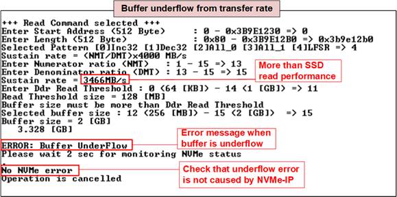
Figure 2‑6 Buffer overflow from too high transfer rate
Figure 2‑6 shows error message when buffer is overflow when the write rate is higher than the SSD performance. The maximum buffer size is applied in this case. Therefore, the user should reduce the transfer rate and tune the value until the buffer is not overflow. As shown in Figure 2‑2, this SSD can run correctly when the write speed is 2285 MB/s.
The next issue that can be caused the overflow problem is setting too low buffer size, as shown in Figure 2‑7.
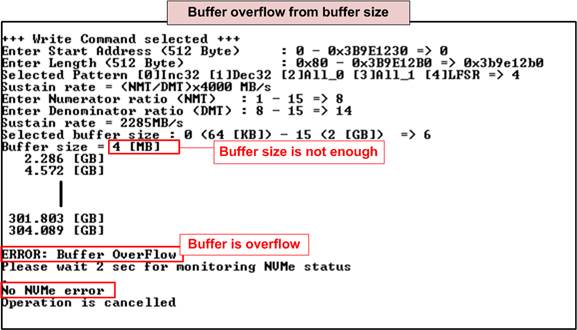
Figure 2‑7 Buffer overflow from too less buffer size
In Figure 2‑2, this SSD can be written at 2285 MB/s with full disk size correctly by using 8.526 MB buffer size. In Figure 2‑7, only 4 MB buffer size is set, so it is not enough for storing the write data while the SSD is busy. Finally, the buffer is overflow. Typically, the buffer usage is increased when the write rate is increased. Thus, the user needs to determine the target write performance and the buffer size requirement in the system.
Besides, if the NVMe-IP detects some errors while operating with the SSD, the data will be stopped. After that, the buffer will be overflow. Therefore, the test console shows 2-sec waiting time (Timeout value of NVMe-IP setting in HDL code of the reference design) after buffer overflow is found. This step is designed to confirm that the buffer overflow is not caused by NVMe-IP error. “No NVMe Error” is shown when there is no error from NVMe.
When error is found, the operation of previous command in NVMe SSD does not finish in a good sequence. It is recommended to power-off/on the adapter board and press “RESET” button to restart the system. For the next trial after buffer overflow, please set the lower transfer rate or larger buffer size to solve the problem before running the test.
2.3 Read Command
Select ‘2’ to send Read command to NVMe SSD.
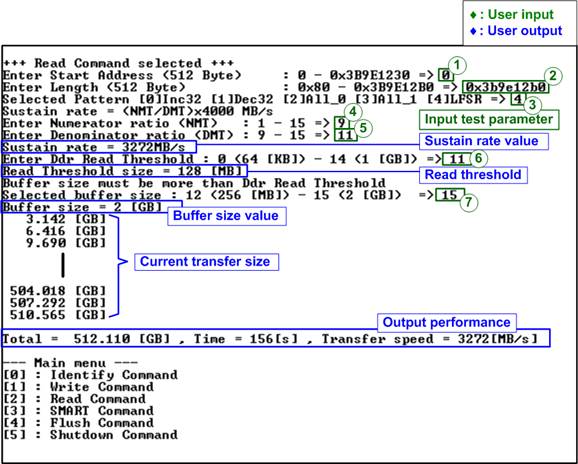
Figure 2‑8 Test result when running Read command
User inputs seven parameters as follows.
1) Start Address: Input start address to read SSD as 512-byte unit. The input is decimal unit when user enters only digit number. User can add “0x” to be prefix for hexadecimal unit. When LBA unit of SSD is 4 Kbyte, this input must be aligned to 8.
2) Transfer Length: Input total transfer size as 512-byte unit. The input is decimal unit when user enters only digit number. User can add “0x” to be prefix for hexadecimal unit. When LBA unit of SSD is 4 Kbyte, this input must be aligned to 8.
3) Test pattern: Select test data pattern to verify data from SSD. Test pattern must be matched with the pattern using in Write Command menu. There are five patterns, i.e., 32-bit incremental, 32-bit decremental, all-0, all-1, and 32-bit LFSR counter
4) Numerator ratio (NMT): Input numerator of transfer rate ratio. Valid value is 1 to 15.
5) Denominator ratio (DMT): Input denominator of transfer rate ratio. Valid value is NMT input to 15. The equation to set the transfer rate is as follows.
Transfer rate (MB/s) = (NMT/DMT) x 4000 (250 MHz x 128-bit)
Note: 4000 is the test data performance in the hardware which uses 250 MHz for transferring 128-bit data. Therefore, the maximum rate is 250 MHz x 128-bit = 4000 MB/s.
Thus, when NMT=9 and DMT=11, the transfer rate is 9/11 x 4000 = 3272 MB/s.
6) Ddr Read Threshold: The minimum data size is stored in DDR before starting reading data from DDR to verify at sustain rate. Valid value is 0 – 15. The mapped table from the set value to buffer size is shown Table 2‑1.
7) Buffer size: Input buffer size to use in this transfer. Valid value is 0-15. The mapped table from the set value to buffer size is shown Table 2‑1. This value must be more than Ddr Read Threshold.
Similar to Write command menu, test system reads data from SSD when all inputs are valid. While reading data, current transfer size is displayed on the console every second to show the progress of transferring. Total size, total time usage, and test speed are displayed after finishing the operation.
“Invalid input” is displayed when some inputs are invalid or unaligned to 8 (when connecting to 4-KB LBA SSD).
Figure 2‑9 shows error message when data verification is failed. “Verify fail” is displayed with the information of the 1st failure data, i.e., the error byte address, the expected value, and the read value.
User can press any key(s) to cancel read operation. Otherwise, the operation is still run until finishing Read command. After that, the output performance is displayed on the console.
When cancelling the operation, the read command still runs as the background process and may not finish in a good sequence. It is recommended to power-off/on FPGA board and adapter board (if connected).
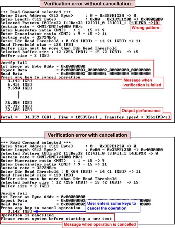
Figure 2‑9 Data verification is failed
When the read rate is too high until the SSD cannot fill the new data to the buffer in time, the buffer in the test system will be underflow. The SSD may pause data transmission in Read command while transferring data for long time. Finally, the buffer is underflow when the pause time is long.
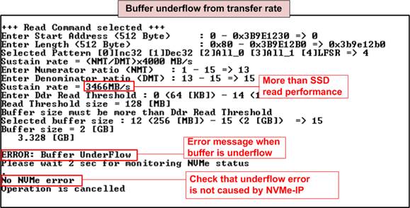
Figure 2‑10 Buffer underflow from too high transfer rate
Figure 2‑10 shows error message when buffer is underflow when the read rate is higher than the SSD performance. The maximum buffer size is applied in this case. Therefore, the user should reduce the transfer rate and tune the value until the buffer is not underflow. As shown in Figure 2‑8, this SSD can run correctly when the write speed is 3272 MB/s.
Similar to Write command, if the user sets too low buffer size, the underflow can be found, as shown in Figure 2‑11.
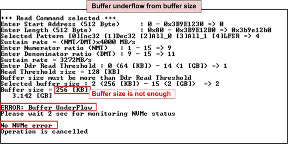
Figure 2‑11 Buffer underflow from too less buffer size
If the NVMe-IP detects some errors while operating with the SSD, the data will be stopped. After that, the buffer will be underflow. Therefore, the test console shows 2-sec waiting time (Timeout value of NVMe-IP setting in HDL code of the reference design) after buffer underflow is found. This step is designed to confirm that the buffer underflow is not caused by NVMe-IP error. “No NVMe Error” is shown when there is no error from NVMe.
When error is found, the operation of previous command in NVMe SSD does not finish in good sequence. It is recommended to power-off/on the adapter board and press “RESET” button to restart the system. For the next trial after buffer underflow, please set the lower transfer rate or larger buffer size to solve the problem before running the test.
2.4 SMART Command
Select ‘3’ to send SMART command to NVMe SSD.
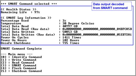
Figure 2‑12 Test result when running SMART command
After finishing the operation, SMART/Health Information (output from SMART command) is displayed as shown in Figure 2‑12. The console shows Health status and SMART log information. Health status shows the remaining life of the SSD in percent unit which is calculated from Percentage Used in the SMART log information.
The SMART log information shows seven parameters as follow.
1) Percentage used: Display SSD usage in percent unit.
2) Temperature in °C unit.
3) Total Data Read decoded as GB/TB unit. Also, raw data without decoding is displayed as 128-bit hexadecimal unit. The unit size of raw data is 512,000 bytes.
4) Total Data Written decoded as GB/TB unit. Also, raw data without decoding is displayed as 128-bit hexadecimal unit. The unit size of raw data is 512,000 bytes.
5) Power On Cycles: Display the number of power cycles.
6) Power On Hours: Display the period of time in hours to show how long the SSD has been powered on.
7) Unsafe Shutdowns: Display the number of unsafe shutdowns of SSD.
2.5 Flush Command
Select ‘4’ to send Flush command to NVMe SSD.
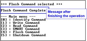
Figure 2‑13 Test result when running Flush command
“Flush Command Complete” is displayed after finishing Flush operation.
2.6 Shutdown Command
Select ‘5’ to send Shutdown command to NVMe SSD.
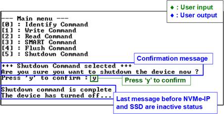
Figure 2‑14 Test result when running Shutdown command
The confirmation message is displayed on the console. User enters ‘y’ or ‘Y’ to continue the operation or enters other keys to cancel the operation.
After finishing Shutdown operation, “Shutdown command is complete” is displayed on the console as the last message. Main menu is not displayed anymore. User needs to power off/on test system to start new test operation.
3 Revision History
|
Revision |
Date |
Description |
|
1.2 |
4-Aug-22 |
Support buffer size setting |
|
1.1 |
25-Mar-21 |
- Remove FPGA setup from the document - Add SMART, Flush, and Shutdown command |
|
1.0 |
19-Apr-18 |
Initial version release |