NVMe-IP DDR reference design manual
Rev1.3 11-Aug-23
2.2.2 Integrated Block for PCIe
3.1 Test firmware (nvmeddrtest.c)
3.2 Function list in Test firmware
1 Introduction

Figure 1‑1 NVMe-IP with and without DDR demo comparison
This reference design is modified from standard NVMe-IP demo by using DDR to be data buffer instead of FIFO, as shown in yellow block of Figure 1‑1 . DDR is applied to the system that requires large data buffer to transfer data as sustain rate but the used SSD has long pause time while writing the data.
In Write command, some SSDs has long pause time which cannot accept more Write data from user logic. During SSD pause time, the data from the source (TestGen) must be stored in data buffer. If the SSD is paused for long time, the buffer size must be large enough by using DDR instead of FIFO. The minimum buffer size is equal to (the maximum pause time of SSD in Write command x data input rate). This is general requirement for data logger system.
In Read command, data from SSD is stored in DDR before forwarding to user logic (TestGen). Sometimes SSD may pause data transmission, so the buffer must have enough data for user reading until the SSD transfers the next read data. Similar to Write command, the minimum buffer size is equal to (the maximum pause time of SSD in Read command x data output rate). The application that requires to read data as sustain rate is the high-resolution display system.
Note: More information of NVMe-IP demo that uses FIFO can be download from following link.
https://dgway.com/products/IP/NVMe-IP/dg_nvmeip_refdesign_en.pdf
2 Hardware overview
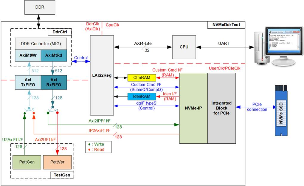
Figure 2‑1 NVMe-IP with DDR demo hardware
The hardware system can be divided to four groups following the function, i.e., Test function (TestGen), DDR controller (DdrIP, AxiMtWr, AxiMtRd, AxiTxFIFO, and AxiRxFIFO), NVMe function (IdenRAM, CtmRAM, NVMe-IP, and PCIe block), and CPU system (CPU and LAxi2Reg). Similar to standard NVMe-IP demo, TestGen generates and verifies test data with NVMe-IP. However, it is modified to transfer data at constant rate instead of the best performance rate. The data is transferred with DDR, the system data buffer. The clock frequency of TestGen and NVMe-IP user interface use the same clock as PCIe clock frequency, 250 MHz.
The user interface of DDR controller is AXI4 bus which has 512-bit data and runs at 300 MHz.
AxiMtWr and AxiMtRd are designed to transfer data between DDR and AxiFIFO in Write command and Read command, respectively. AxiTxFIFO and AxiRxFIFO are asynchronous FIFO and asymmetric FIFO for interface between 512-bit on AXI4 bus and 128-bit on NVMe/TestGen.
IdenRAM and CtrmRAM are included for running Identify command and SMART command respectively. The NVMe command can be selected by the user which is controlled via Serial console. UART interface is a part of CPU system. The user can configure some test parameters such as the data rate of TestGen, the buffer size, NVMe command � Write, Read, etc., and the parameters for running the command. CPU interface with hardware is AXI4-Lite bus, so LAxi2Reg is the adapter logic to convert AXI4-Lite bus to be register interface for controlling the hardware. More details of the hardware are described as follows.
2.1 TestGen

Figure 2‑2 TestGen interface
TestGen module is the test logic to send test data to DDR through AxiTxFIFO when operating Write command. On the other hand, the test data is applied to be the expected value to verify the read data from DDR through AxiRxFIFO when operating Read command. Besides, the duty cycle for asserting write enable and read enable of FIFO are controlled by pulse-width control logic. The duty cycle of enable time is set by the user. The error is asserted if AxiTxFIFO is overflow or AxiRxFIFO is underflow.
Register file in the TestGen receives test parameters from user, i.e., total transfer size, transfer direction, and test pattern. To control transfer size, the counter is designed to count total amount of transferred data. The details of hardware logic within TestGen module are shown in Figure 2‑3.
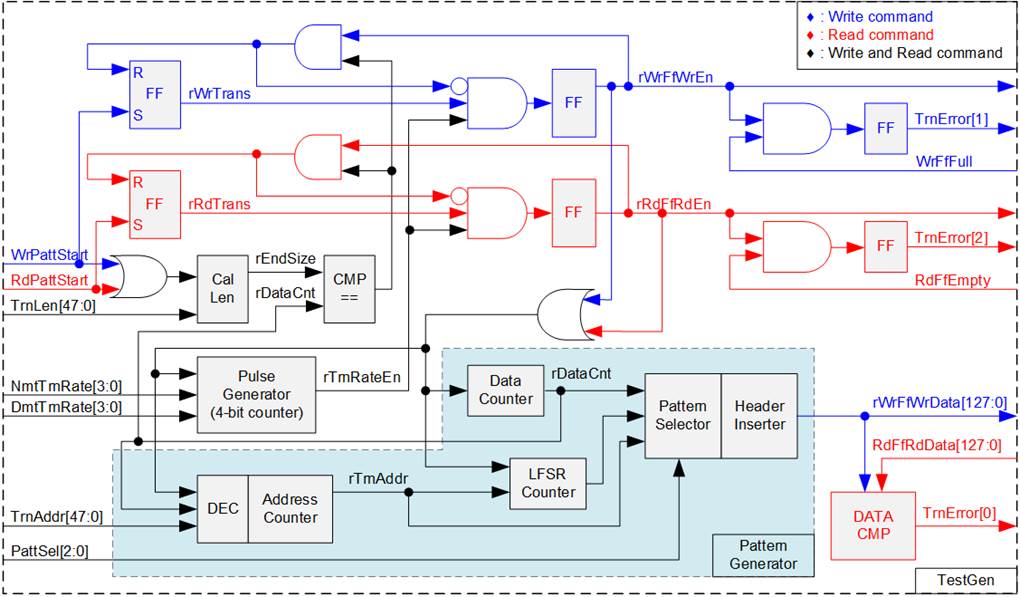
Figure 2‑3 TestGen hardware
The main feature of TestGen is to control data rate for transferring with FIFO to check the best write performance and read performance of the SSDs in sustain rate. The user sets two parameters, NmtTrnRate and DmtTrnRate which are 4-bit signals. Next, Pulse Generator (4-bit counter) loads both parameters and then asserts enable pulse (rTrnRateEn) for NmtTrnRate cycles in every DmtTrnRate cycle. Therefore, transfer data rate for writing FIFO and reading FIFO is equal to (NmtTrnRate/DmtTrnRate) x Clock Frequency (300 MHz) x 128-bit or (NmtTrnRate/DmtTrnRate) x 4800 Mbyte/sec, as shown in Figure 2‑4.
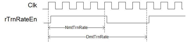
Figure 2‑4 rTrnRateEn Timing diagram
After that, rTrnRateEn is fed to the logic for asserting FIFO write enable or FIFO read enable. Timing diagram to assert rWrFfWrEn and rRdFfRdEn is shown in Figure 2‑5.

Figure 2‑5 rWrTrans/rRdTrans Timing diagram
1) When user sets command register to start Write/Read command, WrPattStart/RdPattStart is asserted to �1� for one cycle. After that, rWrTrans/rRdTrans is asserted to �1� until the operation is done, monitored by rDataCnt.
2) While transferring data, rWrFfWrEn/rRdFfRdEn is asserted to �1� when rTrnRateEn=�1� and rWrTrans/rRdTrans=�1�.
3) To control the amount of transferred data, the data counter (rDataCnt) is counted when rWrFfWrEn/rRdFfRdEn is asserted to �1�.
4) rDataCnt is counted from 0 to N-1 for transferring N data. EndSize value is set by (total transfer size � 1). rWrTrans/rRdTrans and rWrFfWrEn/rRdFfRdEn are de-asserted to �0� when the last data (rDataCnt=EndSize) is transferred to FIFO.
While transferring data to FIFO, the error monitoring logic is operating. When running Write command, WrFfFull is monitored. TrnError[1] is overflow error flag which is asserted to �1� when WrFfFull is equal to �1�. Also, when running Read command, RdFfEmpty is monitored. TrnError[2] is underflow error flag which is asserted to �1� when RdFfEmpty is equal to �1� but Read operation is not finished. If TrnError[1] or [2] is asserted, it is expected that the transfer rate is more than the SSD characteristic. The user should try to reduce the transfer rate until there is no error flag asserted.
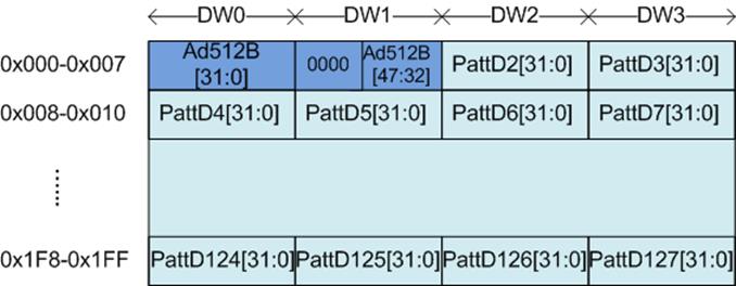
Figure 2‑6 Test pattern format in each 512-byte data for Increment/Decrement/LFSR pattern
Pattern Generator block creates test data for writing to FIFO (rWrFfWrData) in Write command or using to be expected data to compare to read data from FIFO (RdFfRdData) in Read command. There are five patterns that can be selected, controlled by PattSel, i.e., all zero, all one, 32-bit incremental pattern, 32-bit decremental pattern, and LFSR pattern. When creating all-zero or all-one pattern, every bit of data is set to zero or one, respectively. While other patterns are designed by separating the data as two parts to create unique test data in every 512-byte data, as shown in Figure 2‑6.
512-byte data consists of 64-bit header in Dword#0 and Dword#1 and the test data in remaining words of 512-byte data (Dword#2 � Dword#127). The header is created by using the address in 512-byte unit, the output of Address counter block (rTrnAddr). The initial value of the address counter is set by user and the value is increased when finishing transferring each 512-byte data. Remaining Dwords (DW#2 � DW#127) depends on pattern selector which may be 32-bit incremental data, 32-bit decremental data, or LFSR counter. 32-bit incremental data is designed by using the data counter (rDataCnt). The decremental data is designed by connecting NOT logic to incremental data.
The LFSR pattern is designed by using LFSR counter. The equation of LFSR is x^31 + x^21 + x + 1. To create 128-bit LFSR data, the look-ahead technique is applied for generate four 32-bit LFSR data within one clock cycle.
When running Read command, TrnError[0] is designed to be data verification fail flag. This bit is asserted to �1� when the received data (RdFfRdData) is not equal to expected data.
2.2 NVMe
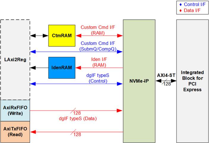
Figure 2‑7 NVMe hardware
Figure 2‑7 shows the interface of NVMe-IP in the reference design. The user interface of NVMe-IP consists of control interface and data interface. The control interface receives the command and the parameters via dgIF typeS or custom command interface, depending on the command. Custom command interface is applied when the command is SMART command or Flush command. Otherwise, dgIF typeS is applied.
The data interface of NVMe-IP has four signal groups, i.e., FIFO input interface (dgIF typeS), FIFO output interface (dgIF typeS), custom command RAM interface, and Identify interface. All data bus width is 128-bit. The custom command RAM interface is bi-directional interface while the others are one directional interface. In the reference design, the custom command RAM interface is used to transfer data of SMART command from NVMe-IP to LAxi2Reg only. Another direction is not used.
2.2.1 NVMe-IP
NVMe-IP implements NVMe protocol of the host side to access one NVMe SSD directly without PCIe switch connection. NVMe-IP supports six commands, i.e., Write, Read, Identify, Shutdown, SMART, and Flush. NVMe-IP can connect to the PCIe hard IP directly. More details of NVMe-IP are described in datasheet.
https://dgway.com/products/IP/NVMe-IP/dg_nvme_ip_data_sheet_en.pdf
2.2.2 Integrated Block for PCIe
This block is the hard IP in Xilinx device which implements Physical, Data Link, and Transaction Layers of PCIe specification. More details are described in Xilinx document.
PG054: 7 Series FPGAs Integrated Block for PCI Express
PG023: Virtex-7 FPGA Gen3 Integrated Block for PCI Express
PG156: UltraScale Devices Gen3 Integrated Block for PCI Express
PG213: UltraScale+ Devices Integrated Block for PCI Express
2.2.3 Dual port RAM
Two dual port RAMs, CtmRAM and IdenRAM, store data from Identify command and SMART command, respectively. IdenRAM is simple dual-port RAM which has one read port and one write port. The data size of Identify command is 8 Kbytes, so IdenRAM size is 8Kbyte. NVMe-IP and LAxi2Reg have different data bus size, so IdenRAM is asymmetric RAM that has the different bus size for write port and read port. The data interface of NVMe-IP (write port) is 128-bit while the interface of LAxi2Reg (read port) is 32-bit. Besides, NVMe-IP has double word enable to write only 32-bit data in some cases. The RAM setting on Xilinx IP wizard supports the write byte enable. Therefore, small logic is designed to convert double word enable to be write byte enable as shown in Figure 2‑8
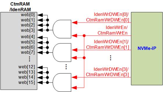
Figure 2‑8 Byte write enable conversion logic
Bit[0] of WrDWEn with WrEn signal are the inputs to AND logic. The output of AND logic is fed to bit[3:0] of IdenRAM byte write enable. Bit[1], [2], and [3] of WrDWEn are applied to be bit[7:4], [11:8], and [15:12] of IdenRAM write byte enable, respectively.
Comparing with IdenRAM, CtmRAM is implemented by true dual-port RAM (two read ports and two write ports) with byte write enable. The small logic to convert double word enable of custom interface to be byte write enable must be used, similar to IdenRAM. True dual-port RAM is used to support the additional features when the customized custom command needs the data input. To support SMART command, using simple dual port RAM is enough. Though the data size returned from SMART command is 512 bytes, CtmRAM is implemented by 8Kbyte RAM for customized custom command.
2.3 DdrCtrl
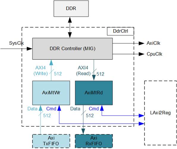
Figure 2‑9 DdrCtrl hardware
This module is designed to interface with DDR memory which is the data buffer to support transferring data as sustain rate in this system. MIG is Xilinx IPcore to control external memory such as DDR4. The IP includes clock generator to generate many clock sources for interface with DDR. This reference design uses clock generator inside MIG to generate CpuClk (100 MHz) for running CPU and its peripherals. AxiClk is clock output from MIG to be user interface of DDR controller. AxiClk frequency is 300 MHz for running DDR4 at 1200 MHz.
AxiMtWr and AxiMtRd decode the command request from LAxi2Reg. After that, data is transferred between MIG and AxiTxFIFO/AxiRxFIFO, following the current command (Write or Read). AxiMtWr and AxiMtRd are designed to be AXI4 master mode for connecting with DDR which is run in Slave mode by using 512-bit data bus. Two master channels are created to connect with AxiMtWr and AxiMtRd. Though AXI4 interface supports bi-directional transferring, only one direction is applied for AxiMtWr/AxiMtRd. AxiMtWr is designed to Write DDR while AxiMtRd is designed to read DDR. All AXI4 modules are run in AxiClk domain.
2.3.1 AxiMtWr
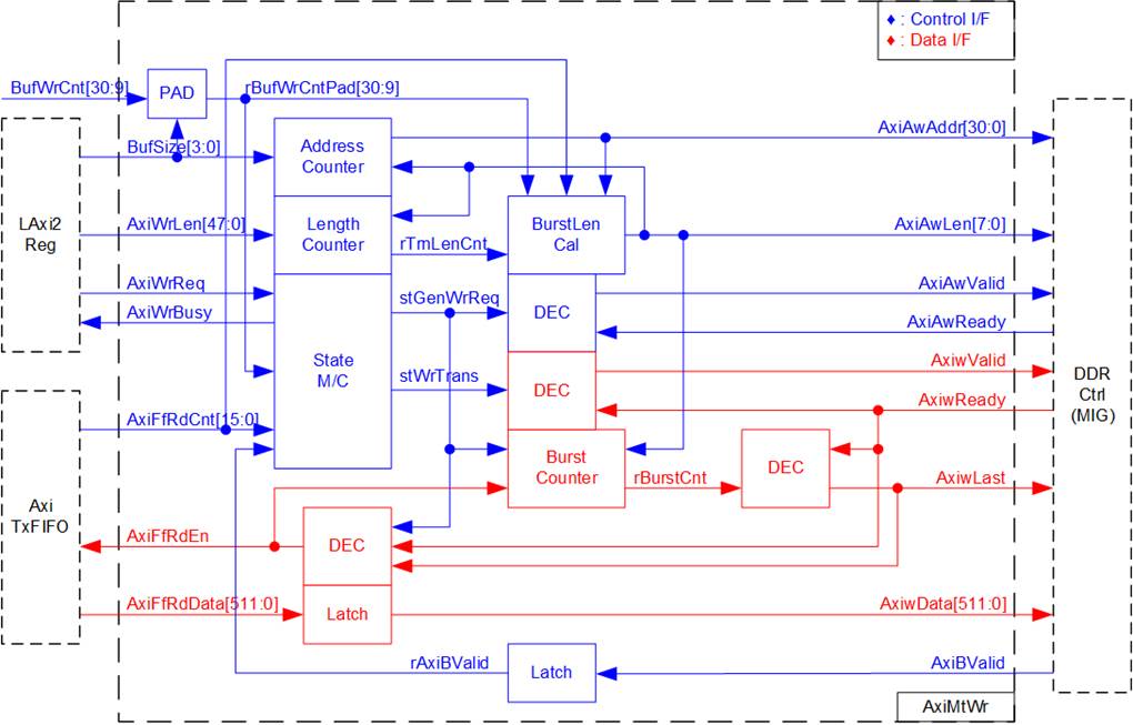
Figure 2‑10 AxiMtWr hardware
AxiMtWr receives BufSize signal to specify the buffer size usage in this transfer. 4-bit signal is applied to select 16 buffer sizes, starting from 64 Kbytes to 2 Gbytes. The core engine of AxiMtWr is state machine which handles to generate write request to DDR and start data transferring from AxiTxFIFO to DDR. As shown in Figure 2‑10, the interface of AxiMtWr is separated to two groups, i.e., command interface and data interface.
The sequence of write transaction by using AXI4 interface is as follows.
1) Send address and address control signals (AxiAwAddr, AxiAwLen, and AxiAwValid)
2) Send data and data control signals (AxiwData and AxiwValid)
3) Wait response (AxiBValid).
From above specification, six state machines are designed to be the core controller.
1) stIdle: This is the first state which receives the write request from LAxi2Reg (AxiWrReq). The state changes to the next state (stChkWrRdy) when the new request is received. At the same time, Length counter loads total transfer size from AxiWrLen and Address counter is reset to 0.
2) stChkWrRdy: This state waits until AxiTxFIFO and DDR buffer are ready for transferring data. At least 512-byte data must be available in AxiTxFIFO, monitored from AxiFfRdCnt. Also, rBufWrCntPad (the signal to show the amount of data in the buffer) is read to confirm that free space in DDR is more than 512 bytes. After that, it changes to the next state, stGenWrReq.
3) stGenWrReq: This state generates write request to DDR (AxiAwValid). Also, other parameters, write address (AxiAwAddr) and write length (AxiAwLen), must be valid. It changes to the next state, stWrTrans, when the MIG accepts the request by asserting AxiAwReady to �1�.
4) stWrTrans: This state transfers the data to DDR. AxiFfRdEn is asserted to �1� to read data from FIFO. After that, the read data (AxiFfRdData) is loaded to the latch register to be the output of AxiwData. At the same time, AxiwValid is asserted to �1� to be data valid for DDR. Two-step pipeline registers in data path are designed to solve timing constraint problem. rBurstCnt counts the amount of data in the current burst transfer. Data transfer state is completed after rBurstCnt shows that current data is the last data. AxiwLast is asserted to �1� for sending the last data in the burst transfer. After that, it changes to the next state, stWtResp.
5) stWtResp: This state waits the response returned from DDR to confirm the previous data transferring is completed. AxiBValid is asserted to �1� by MIG if DDR receives all write data completely. After that, the remaining transfer size (rTrnLenCnt) is read. If rTrnLenCnt is not equal to 0, the next state is stWtBufCnt. Otherwise, the state is returned to stIdle. rTrnLenCnt loads total transfer size from AxiWrLen when receiving the request from LAxi2Reg. rTrnLenCnt is decreased after finishing each burst transfer loop.
6) stWtBufCnt: This state is run for one clock cycle to wait until rBufWrCntPad is updated and ready for using in stChkWrRdy. Next, it returns to stChkWrRdy to start transferring the next data.
From above sequence, address, data, and response in each burst loop are run sequentially by using one state machine, not pipelined transferring for simple design. To improve transfer performance, the burst size of each loop can be set by four values, i.e., 512 bytes, 1024 bytes, 2048 bytes, and 4096 bytes. The value of burst size (AxiAwLen) is calculated by BurstLenCal block. The burst size depends on several conditions. First, the amount of available data in AxiTxFIFO (monitored by AxiFfRdCnt) and the free space size in DDR (monitored by rBufWrCntPad). Second, the value of AxiAwAddr that must be aligned to the burst size to avoid overlapped DDR area. Last is the remaining transfer size, rTrnLenCnt. For example, burst size is set to 4096 bytes when following conditions are met.
i) Remaining transfer size (rTrnLenCnt) is more than or equal to 4096 bytes (Bit[47:3] of rTrnLenCnt is not equal to 0).
ii) Current write address (AxiAwAddr) is aligned to 4096 bytes (Bit[11:0] of AxiAwAddr is equal to 0).
iii) Data in AxiTxFIFO (AxiFfRdCnt) is more than or equal to 4096 bytes (Bit[15:6] of AxiFfRdCnt is not equal to 0).
iv) Data in DDR (rBufWrCntPad) has at least 8 Kbyte free space (Bit[30:13] of rBufWrCntPad is not equal to all 1).
After AxiAwLen is completely calculated, this signal is fed to Address counter to calculate the next write address (AxiAwAddr). Also, it is fed to Length Counter to calculate remaining transfer size (rTrnLenCnt).
Figure 2‑11 shows the example operation of AxiMtWr when burst size is equal to 8 for transferring 512-byte data.
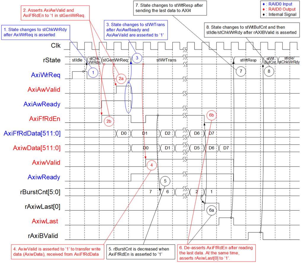
Figure 2‑11 AxiMtWr Timing diagram when burst size = 512 byte
1) After AxiWrReq is asserted to �1�, state machine changes to stChkWrRdy.
2) If FIFO and DDR are ready to transfer 512-byte data, state machine will change to next state, stGenWrReq. Two functions are run in stGenWrReq. First, asserts Write request (AxiAwValid) to �1� until AxiAwReady is asserted to �1�. Second, asserts AxiFfRdEn to 1 for two clock cycles to read two data from AxiTxFIFO.
3) After write request is received (AxiAwValid=�1� and AxiAwReady=�1�), state machine changes to stWrTrans.
4) Eight data is transferred in stWrTrans by asserting AxiwValid to �1� for 8 cycles. At the same time, AxiwData is valid by loading the previous data from AxiFfRdData.
5) While transferring data, rBurstCnt is decreased by AxiFfRdEn signal.
6) When rBurstCnt=2 and AxiwReady=�1�, rAxiwLast[0] is asserted to �1� to pause data reading from FIFO by de-asserting AxiFfRdEn to �0�. After that, AxiwLast (the previous status of rAxiwLast[0]) is asserted to �1� with the last data available on the bus to complete data transfer.
7) State machine changes to stWtResp to wait until AxiBValid asserting to �1�.
8) State machine changes to stWtBufCnt which is run for one cycle.
9) State machine enters to stIdle when total data are transferred. Otherwise, state machine returns to stChkWrRdy to start transferring the next data.
2.3.2 AxiMtRd
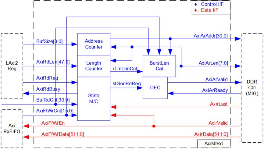
Figure 2‑12 AxiMtRd hardware
Similar to AxiMtWr, AxiMtRd receives BufSize signal to specify the buffer size usage in this transfer. 4-bit signal is applied to select 16 buffer sizes, starting from 64 Kbytes to 2 Gbytes.
The core engine of AxiMtRd is state machine which handles to generate read request to DDR and wait until the data is returned from DDR. As shown in Figure 2‑12, the interface of AxiMtRd is separated to two groups, i.e., command interface and data interface.
The sequence of read transaction by using AXI4 interface is as follows.
1) Send address and address control signals (AxiArAddr, AxiArLen, and AxiArValid)
2) Receive data and data control signals (AxirValid, AxirLast, and AxirData)
From above specification, four state machines are designed to be the core controller.
1) stIdle: This is the first state which receives the read request from LAxi2Reg (AxiRdReq). The state changes to the next state (stChkRdRdy) when the new request is received. At the same time, Length counter loads total transfer size from AxiRdLen and Address counter is reset to 0.
2) stChkRdRdy: This state has two functions. First, check remained transfer length (rTrnLenCnt). If total data are completely transferred (rTrnLenCnt=0), the next state will be stIdle. Otherwise, it prepares to transfer the data by monitoring buffer status. Therefore, the second function of this state is checking that AxiRxFIFO and DDR buffer are ready for transferring data. At least 512-byte data must be available in DDR, monitored from BufRdCnt. Also, AxiFfWrCnt is read to confirm that free space in AxiRxFIFO is more than 512 bytes. After that, it changes to the next state, stGenWrReq.
3) stGenRdReq: This state generates read request to DDR (AxiArValid). Also, other parameters, read address (AxiArAddr) and read length (AxiArLen), must be valid. It changes to the next state, stRdTrans, when the MIG accepts the request by asserting AxiArReady to �1�.
4) stRdTrans: This state transfers the data from DDR to AxiRxFIFO. Read data (AxirData) and Read data valid (AxirValid) are fed to be write data and write enable of AxiRxFIFO (AxiFfWrData and AxiFfWrEn). After receiving the last data of the burst transfer (AxirValid=�1� and AxirLast=�1�), the state returns to stChkRdRdy.
Similar to AxiMtWr, the burst size of each loop can be set by four values, i.e., 512 bytes, 1024 bytes, 2048 bytes, and 4096 bytes. The value of burst size (AxiArLen) is calculated by BurstLenCal block. The burst size depends on several conditions. First, the amout of available data in DDR (monitored by BufRdCnt) and the free space size in AxiRxFIFO (monitored by AxiFfWrCnt). Second, the value of AxiArAddr that must be aligned to the burst size to avoid overlapped DDR area. Last is the remaining transfer size, rTrnLenCnt. For example, burst size is set to 4096 bytes when following conditions are met.
i) Remaining transfer size (rTrnLenCnt) is more than or equal to 4096 bytes (Bit[47:3] of rTrnLenCnt is not equal to 0).
ii) Current read address (AxiArAddr) is aligned to 4096 bytes (Bit[11:0] of AxiArAddr is equal to 0).
iii) Data in DDR (BufRdCnt) is more than or equal to 4096 bytes (Bit[30:12] of BufRdCnt is not equal to 0).
iv) Data in AxiRxFIFO (AxiFfWrCnt) has at least 8 Kbyte free space (Bit[15:7] of AxiFfWrCnt is not equal to all 1).
After AxiArLen is completely calculated, this signal is fed to Address counter to calculate the next write address (AxiArAddr). Also, it is fed to Length Counter to calculate the remaining transfer size (rTrnLenCnt).
Figure 2‑13 shows the example operation of AxiMtRd when burst size is equal to 8 for transferring 512-byte data.
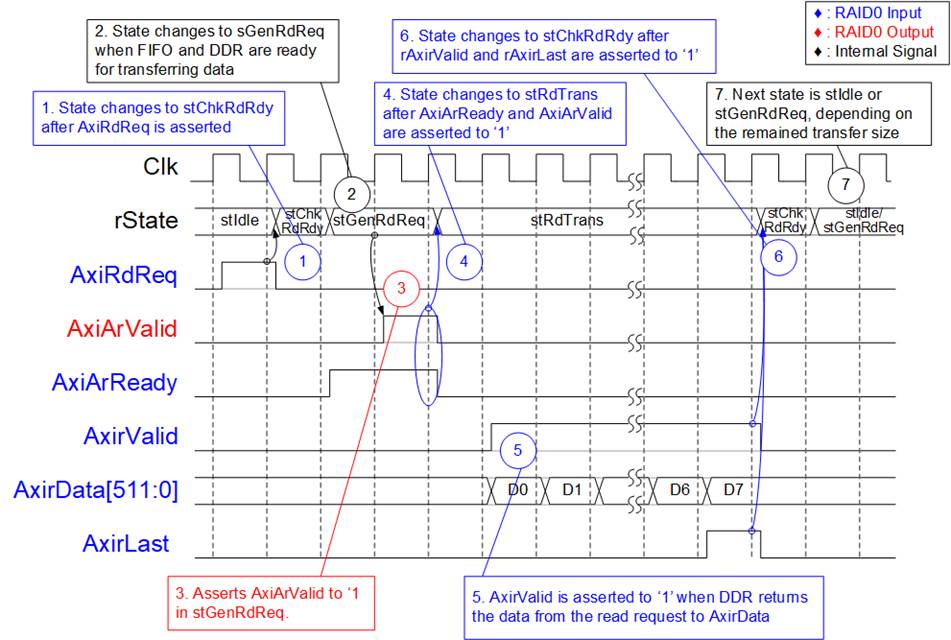
Figure 2‑13 AxiMtRd Timing diagram when burst size = 512 byte
1) After AxiRdReq is asserted to �1�, state machine changes to stChkRdRdy.
2) If available data in DDR is at least 512 bytes and free space in AxiRxFIFO is more than 512 bytes, it will change to the next state, stGenRdReq, for starting data transferring.
3) AxiArValid is asserted to �1� to generate read request to DDR.
4) AxiArValid is de-asserted to �0� after DDR accepts the request by asserting AxiArReady to �1�. Also, state machine changes to stRdTrans.
5) Eight data is transferred in stRdTrans by asserting AxirValid to �1� for 8 cycles. At the same time, AxirData is valid. AxirData are forwarded to store to AxiRxFIFO.
6) AxirLast and AxirValid are asserted to �1� when the last data of the burst transfer are transferred from DDR. After that, the state returns to stChkRdRdy.
7) Before starting the new transfer loop, the remained transfer length (rTrnLenCnt) is read. If rTrnLenCnt is equal to 0, the next state will be stIdle to complete the operation. Otherwise, repeat step 2 to wait until FIFO and DDR are ready for data transferring.
2.4 CPU and Peripherals
32-bit AXI4-Lite bus is applied to be the bus interface for CPU accessing the peripherals such as Timer and UART. The test system of NVMe-IP connects with CPU as a peripheral on 32-bit AXI4-Lite bus for CPU controlling and monitoring. CPU assigns the different base address and the address range to each peripheral for accessing one peripheral at a time.
In the reference design, the CPU system is built with one additional peripheral to access the test logic. Therefore, the hardware logic must be designed to support AXI4-Lite bus standard for CPU writing and reading. LAxi2Reg module is designed to connect with the CPU system as shown in Figure 2‑14.
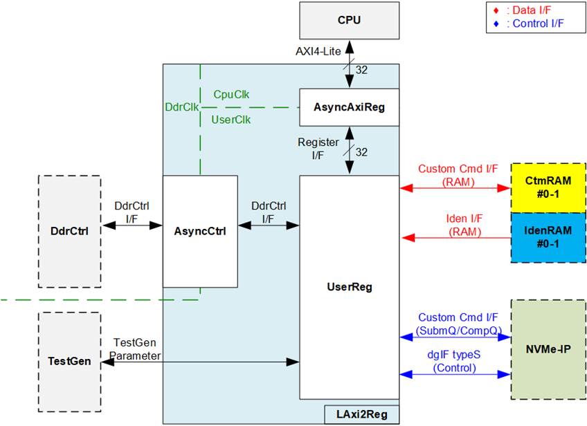
Figure 2‑14 CPU and peripherals hardware
LAxi2Reg consists of AsyncAxiReg, UserReg, and AsyncCtrl. AsyncAxiReg is designed to convert the AXI4-Lite signals to be the simple register interface which has 32-bit data bus size, similar to AXI4-Lite data bus size. Besides, AsyncAxiReg includes asynchronous logic to support clock domain crossing between CpuClk domain and UserClk domain.
UserReg includes the register file of the parameters and the status signals to control the other modules, i.e., CtmRAM, IdenRAM, NVMe-IP, TestGen, and DdrCtrl I/F.
While clock domain of DdrCtrl is DdrClk, clock domain of UserReg is UserClk. Therefore, AsyncCtrl includes asynchronous logic to support clock domain crossing between between DdrClk domain and UserClk domain. More details of each hardware are described as follows.
2.4.1 AsyncCtrl
There are two styles to transfer the signal from source clock domain to destination clock domain. First, the signal which is one-bit signal or stable value for long time. The signal is forwarded to D Flip-Flop to synchronous on destination clock domain. Second, the bus signal that has multiple bits. This signal must be fed to latched register to generate stable value. After that, the stable signal is transferred to the destination clock domain by using D Flip-Flop.
2.4.2 AsyncAxiReg

Figure 2‑15 AsyncAxiReg Interface
The signal on AXI4-Lite bus interface can be split into five groups, i.e., LAxiAw* (Write address channel), LAxiw* (Write data channel), LAxiB* (Write response channel), LAxiAr* (Read address channel), and LAxir* (Read data channel). More details to build custom logic for AXI4-Lite bus is described in following document.
According to AXI4-Lite standard, the write channel and the read channel are operated independently. Also, the control and data interface of each channel are run separately. So, the logic inside AsyncAxiReg to interface with AXI4-Lite bus is split into four groups, i.e., Write control logic, Write data logic, Read control logic, and Read data logic as shown in the left side of Figure 2‑15. Write control I/F and Write data I/F of AXI4-Lite bus are latched and transferred to be Write register interface with clock domain crossing registers. Similarly, Read control I/F of AXI4-Lite bus are latched and transferred to be Read register interface while Read data is returned from Register interface to AXI4-Lite through clock domain crossing registers. In Register interface, RegAddr is shared signal for write and read access, so it loads the value from LAxiAw for write access or LAxiAr for read access.
The simple register interface is compatible with single-port RAM interface for write transaction. The read transaction of the register interface is slightly modified from RAM interface by adding RdReq and RdValid signals for controlling read latency time. The address of register interface is shared for write and read transaction. Therefore, user cannot write and read the register at the same time. The timing diagram of the register interface is shown in Figure 2‑16.
Figure 2‑16 Register interface timing diagram
1) To write register, the timing diagram is similar to single-port RAM interface. RegWrEn is asserted to �1� with the valid signal of RegAddr (Register address in 32-bit unit), RegWrData (write data of the register), and RegWrByteEn (the write byte enable). Byte enable has four bits to be the byte data valid. Bit[0], [1], [2], and [3] are equal to �1� when RegWrData[7:0], [15:8], [23:16], and [31:24] are valid, respectively.
2) To read register, AsyncAxiReg asserts RegRdReq to �1� with the valid value of RegAddr. 32-bit data must be returned after receiving the read request. The slave must monitor RegRdReq signal to start the read transaction. In read operation, the address value (RegAddr) does not change the value until RegRdValid is asserted to �1�. Therefore, the address can be used for selecting the returned data by using multiple layers of multiplexer.
3) The read data is returned on RegRdData bus by the slave with asserting RegRdValid to �1�. After that, AsyncAxiReg forwards the read value to LAxir* interface.
2.4.3 UserReg
Figure 2‑17 UserReg Interface
The logic inside UserReg consists of Address decoder, RegFile, and RegMux. The address decoder decodes the address which is requested from AsyncAxiReg and then selects the active register for write or read transaction. The address range assigned in UserReg is split into six areas, as shown in Figure 2‑17.
1) 0x0000 � 0x00FF : mapped to set the command with the parameters of NVMe-IP, TestGen, and DdrCtrl. This area is write-access only.
2) 0x0100 � 0x01FF : mapped to read the status signals of NVMe-IP, TestGen, and DdrCtrl. This area is read-access only.
3) 0x0200 � 0x02FF : mapped to set the test parameters of custom command interface. This area is write-access only.
4) 0x0300 � 0x03FF : mapped to read the status of custom command interface. This area is read-access only.
5) 0x2000 � 0x3FFF : mapped to read data from IdenRAM. This area is read-access only.
6) 0x4000 � 0x5FFF : mapped to custom command RAM interface. Although this area supports both write and read access, the demo shows only read access by running SMART command.
Address decoder decodes the upper bit of RegAddr for selecting the active hardware that is NVMe-IP, DdrCtrl, TestGen, Iden RAM, or CtmRAM. The register file inside UserReg is 32-bit bus size. Therefore, write byte enable (RegWrByteEn) is not applied in the test system and the CPU uses 32-bit pointer to set the hardware register.
To read register, two-step multiplexers select the data to return to CPU by using the address. The lower bit of RegAddr is fed to the submodule to select the active data from each submodule. While the upper bit is applied in UserReg to select the returned data from each submodule. Totally, the latency time of read data is equal to two clock cycles. Therefore, RegRdValid is created by RegRdReq with asserting two D Flip-flops. More details of the address mapping within UserReg module are shown in Table 2‑1.
Table 2‑1 Register Map
|
Address |
Register Name |
Description |
|
Rd/Wr |
(Label in �nvmeddrterst.c�) |
|
|
0x0000 � 0x00FF: Status signals of NVMe-IP, TestGen, and DdrCtrl (Write access only) |
||
|
BA+0x000 |
User Address (Low) Reg |
[31:0]: Input to be bit[31:0] of start address in 512-byte unit (UserAddr[31:0] of dgIF typeS for NVMe-IP) |
|
(USRADRL_REG) |
||
|
BA+0x004 |
User Address (High) Reg |
[15:0]: Input to be bit[47:32] of start address in 512-byte unit (UserAddr[47:32] of dgIF typeS for NVMe-IP) |
|
(USRADRH_REG) |
||
|
BA+0x008 |
User Length (Low) Reg |
[31:0]: Input to be bit[31:0] of transfer length in 512-byte unit (UserLen[31:0] of dgIF typeS for NVMe-IP) |
|
(USRLENL_REG) |
||
|
BA+0x00C |
User Length (High) Reg |
[15:0]: Input to be bit[47:32] of transfer length in 512-byte unit (UserLen[47:32] of dgIF typeS for NVMe-IP) |
|
(USRLENH_REG) |
||
|
BA+0x010 |
User Command Reg |
[2:0]: Input to be user command (UserCmd of dgIF typeS for NVMe-IP) 000b: Identify, 001b: Shutdown, 010b: Write SSD, 011b: Read SSD, 100b: SMART, 110b: Flush, 101b/111b: Reserved When this register is written, the command request is sent to NVMe-IP. After that, the IP starts operating the command. |
|
(USRCMD_REG) |
||
|
BA+0x014 |
Test Pattern Reg |
[2:0]: Select test pattern 000b-Increment, 001b-Decrement, 010b-All 0, 011b-All 1, 100b-LFSR |
|
(PATTSEL_REG) |
||
|
BA+0x020 |
NVMe Timeout Reg |
[31:0]: Mapped to TimeOutSet[31:0] of NVMe-IP |
|
(NVMTIMEOUT_REG) |
||
|
BA+0x040 |
Transfer Ratio Reg |
Set the sustain rate for write or read access of TestGen module. [11:8]: the numerator of the ratio, [3:0]: the denominator of the ratio. Transfer Rate (bit/sec) = (Numerator/Denominator) x UserClk (250MHz) x 128-bit |
|
(TRNRATIO_REG) |
||
|
BA+0x044 |
DDR Read threshold |
[3:0]: The threshold value of DDR buffer before starting reading. TestGen module waits until the data in DDR is more than or equal to the threshold value and then it starts reading the data from DDR as sustain rate in Read command. Valid from 0 - 15. 0: 64 Kbyte, 1: 128 Kbyte, 2: 256 Kbyte, 3: 512 Kbyte, 4: 1 Mbyte, 5: 2 Mbyte, 6: 4 Mbyte, 7: 8 Mbyte, 8: 16 Mbyte, 9: 32 Mbyte, 10: 64 Mbyte, 11: 128 Mbyte, 12: 256 Mbyte, 13: 512 Mbyte, 14: 1 Gbyte, 15: 2 Gbyte |
|
(DDRRDTHR_REG) |
||
|
BA+0x048 |
DDR Size Setting Reg |
[3:0]: Setting buffer size for usage. Valid from 0 � 15. The mapped value from 4-bit signal to the buffer size is similar to DDRRDTHR_REG. |
|
DDRBUFFSET_REG |
||
|
0x0100 � 0x01FF: Status signals of NVMe-IP, TestGen, and DdrCtrl (Read access only) |
||
|
BA+0x0100 |
User Status Reg |
[0]: UserBusy of dgIF typeS (�0�: Idle, �1�: Busy) [1]: UserError of dgIF typeS (�0�: Normal, �1�: Error) [2]: Data verification fail (�0�: Normal, �1�: Error) [3]: Error from buffer overflow during Write command (�0�: Normal, �1�: AxiTxFIFO is full during running sustain write) [4]: Error from buffer underflow during Read command (�0�: Normal, �1�: AxiRxFIFO is empty during running sustain read) [5]: Busy flag of write operation from TestGen (�0�: No operation, �1�: Write is operating) [6]: Busy flag of read operation from TestGen (�0�: No operation, �1�: Read is operation) Note that this flag is asserted after data in DDR is equal or more than threshold value, set by DDRRDTHR_REG. [7]: Busy flag of write operation from DdrCtrl (�0�: No operation, �1�: Write is operating) [8]: Busy flag of read operation from DdrCtrl (�0�: No operation, �1�: Write is operating) |
|
(USRSTS_REG) |
||
Address |
Register Name |
Description |
|
Rd/Wr |
(Label in �nvmeddrterst.c�) |
|
|
0x0100 � 0x01FF: Status signals of NVMe-IP, TestGen, and DdrCtrl (Read access only) |
||
|
BA+0x0104 |
Total disk size (Low) Reg |
[31:0]: Mapped to LBASize[31:0] of NVMe-IP
|
|
(LBASIZEL_REG) |
||
|
BA+0x0108 |
Total disk size (High) Reg |
[15:0]: Mapped to LBASize[47:32] of NVMe-IP [31]: Mapped to LBAMode of NVMe-IP |
|
(LBASIZEH_REG) |
||
|
BA+0x010C |
User Error Type Reg |
[31:0]: Mapped to UserErrorType[31:0] of NVMe-IP to show error status |
|
(USRERRTYPE_REG) |
||
|
BA+0x0110 |
PCIe Status Reg |
[0]: PCIe linkup status from PCIe hard IP (�0�: No linkup, �1�: linkup) [3:2]: PCIe link speed from PCIe hard IP. MSB is bit[16]. (000b: Not linkup, 001b: PCIe Gen1, 010b: PCIe Gen2, 011b: PCIe Gen3, 111b: PCIe Gen4) [7:4]: PCIe link width status from PCIe hard IP (0001b: 1-lane, 0010b: 2-lane, 0100b: 4-lane, 1000b: 8-lane) [13:8]: Current LTSSM State of PCIe hard IP. Please see more details of LTSSM value in PCIe hard IP datasheet [16]: The upper-bit to show PCIe link speed of PCIe hard IP. Two lower bits are bit[3:2]. |
|
(PCIESTS_REG)
|
||
|
BA+0x0114 |
Completion Status Reg |
[15:0]: Mapped to AdmCompStatus[15:0] of NVMe-IP [31:16]: Mapped to IOCompStatus[15:0] of NVMe-IP |
|
(COMPSTS_REG) |
||
|
BA+0x0118 |
NVMe CAP Reg |
[31:0]: Mapped to NVMeCAPReg[31:0] of NVMe-IP |
|
(NVMCAP_REG) |
||
|
BA+0x011C |
NVMe IP Test pin Reg |
[31:0]: Mapped to TestPin[31:0] of NVMe-IP |
|
(NVMTESTPIN_REG) |
||
|
BA+0x0130-BA+0x013F |
Expected value Word0-3 Reg |
128-bit of the expected data at the 1st failure data in TestGen when operating Read command 0x0130: Bit[31:0], 0x0134: Bit[63:32], �, 0x013C: Bit[127:96] |
|
(EXPPATW0-W3_REG) |
||
|
BA+0x0140-BA+0x014F |
Read value Word0-3 Reg |
128-bit of the read data at the 1st failure data in TestGen when operating Read command 0x0140: Bit[31:0], 0x0144: Bit[63:32], �, 0x014C: Bit[127:96] |
|
(RDPATW0-W3_REG) |
||
|
BA+0x0150 |
Data Failure Address(Low) Reg |
[31:0]: Bit[31:0] of the byte address of the 1st failure data in TestGen when operating Read command |
|
(RDFAILNOL_REG) |
||
|
BA+0x0154 |
Data Failure Address(High) Reg |
[24:0]: Bit[56:32] of the byte address of the 1st failure data in TestGen when operating Read command |
|
(RDFAILNOH_REG) |
||
|
BA+0x0158 |
Current test byte (Low) Reg |
[31:0]: Bit[31:0] of the current test data size in TestGen module |
|
(CURTESTSIZEL_REG) |
||
|
BA+0x015C |
Current test byte (High) Reg |
[24:0]: Bit[56:32] of the current test data size of TestGen module |
|
(CURTESTSIZEH_REG) |
||
|
BA+0x0160 |
DDR Write Address Reg |
[31:0]: Current DDR write address in byte unit (bit[8:0] is fixed to 0 to align 512-byte unit) |
|
(DDRWRADDR_REG) |
||
|
BA+0x0164 |
DDR Read Address Reg |
[31:0]: Current DDR read address in byte unit (bit[8:0] is fixed to 0 to align 512-byte unit) |
|
(DDRRAADDR_REG) |
||
|
BA+0x016C |
DDR Maximum Size Usage |
[31:0]: The maximum DDR size that is used in Write command. It is calculated by finding the maximum value of (DDRWRADDR_REG � DDRRDADDR_REG). Similar to DDRWR/RDADDR_REG, bit[8:0] is always equal to 0 to align 512-byte unit |
|
(DDRMAXUSED_REG) |
||
Address |
Register Name |
Description |
|
Rd/Wr |
(Label in �nvmeddrterst.c�) |
|
|
Other interfaces (Custom command of NVMe-IP, IdenRAM, and Custom RAM) |
||
|
BA+0x0200-BA+0x023F |
Custom Submission Queue Reg |
[31:0]: Submission queue entry of SMART and Flush command. Input to be CtmSubmDW0-DW15 of NVMe-IP. 0x200: DW0, 0x204: DW1, �, 0x23C: DW15 |
|
Wr |
(CTMSUBMQ_REG) |
|
|
BA+0x0300- BA+0x030F |
Custom Completion Queue Reg |
[31:0]: CtmCompDW0-DW3 output from NVMe-IP. 0x300: DW0, 0x304: DW1, �, 0x30C: DW3 |
|
Rd |
(CTMCOMPQ_REG) |
|
|
BA+0x0800 |
IP Version Reg |
[31:0]: Mapped to IPVersion[31:0] of NVMe-IP |
|
Rd |
(IPVERSION_REG) |
|
|
BA+0x2000- BA+0x2FFF |
Identify Controller Data |
4Kbyte Identify Controller Data Structure |
|
Rd |
(IDENCTRL_REG) |
|
|
BA+0x3000- BA+0x3FFF |
Identify Namespace Data |
4Kbyte Identify Namespace Data Structure |
|
Rd |
(IDENNAME_REG) |
|
|
BA+0x4000- BA+0x5FFF |
Custom command Ram |
Connect to 8K byte CtmRAM interface. Used to store 512-byte data output from SMART Command. |
|
Wr/Rd |
(CTMRAM_REG) |
|
3 CPU Firmware
3.1 Test firmware (nvmeddrtest.c)
After system boot-up, CPU runs following steps to finish the initialization process.
1) CPU initializes its peripherals such as UART and Timer.
2) CPU waits until PCIe connection links up (PCIESTS_REG[0]=�1�).
3) CPU waits until NVMe-IP completes initialization process (USRSTS_REG[0]=�0�). If some errors are found, the process stops with displaying the error message.
4) CPU displays PCIe link status (the number of PCIe lanes and the PCIe speed) by reading PCIESTS_REG[16:2].
5) CPU displays the main menu. There are six menus for running six commands of NVMe-IP, i.e., Identify, Write, Read, SMART, Flush, and Shutdown.
More details of the sequence in each command in CPU firmware are described as follows.
3.1.1 Identify command
The sequence of the firmware when user selects Identify command is below.
1) Set USRCMD_REG[2:0]=000b to send Identify command request to NVMe-IP. After that, busy flag (USRSTS_REG[0]) changes from �0� to �1�.
2) CPU waits until the operation is completed or some errors are found by monitoring USRSTS_REG[1:0].
Bit[0] is de-asserted to �0� after finishing operating the command. After that, the data from Identify command of NVMe-IP is stored in IdenRAM.
Bit[1] is asserted to �1� when some errors are detected. The error message is displayed on the console to show the error details, decoded from USRERRTYPE_REG[31:0]. Finally, the process is stopped.
3) After busy flag (USRSTS_REG[0]) is de-asserted to �0�, CPU displays some information decoded from IdenRAM (IDENCTRL_REG) such as SSD model name and the information from NVMe-IP such as SSD capacity (LBASIZEL/H_REG).
3.1.2 Write/Read command
The sequence of the firmware when user selects Write/Read command is below.
1) Receive start address, transfer length, test pattern, sustain rate, DDR threshold value (DDR threshold is the parameter for Read command only), and DDR size from Serial console. If some inputs are invalid, the operation is cancelled.
Note: If LBA unit size = 4 Kbyte, start address, and transfer length must be aligned to 8.
2) Get all inputs and set the value to USRADRL/H_REG, USRLENL/H_REG, PATTSEL_REG, TRNRATIO_REG, DDRRDTHR_REG, and DDRBUFFSET_REG.
3) Set USRCMD_REG[2:0]=010b for Write command or 011b for Read command and then the command request is asserted. After that, busy flag (USRSTS_REG[0]) changes from �0� to �1�.
4) CPU waits until the operation is completed or some errors (except verification error) are found by monitoring USRSTS_REG[8:0].
Bit[0] and bit[8:5] are de-asserted to �0� when command is completed.
Bit[1] is asserted when some errors are detected. The error message is displayed on the console to show the error details (decoded from USRERRTYPE_REG[31:0]) and then the process is stopped.
Bit[2] is asserted when data verification is failed. The verification error message is displayed on the console to show the error details. In this condition, CPU is still run until the operation is done or user presses any key(s) to cancel operation.
Bit[3] is asserted to �1� when buffer is overflow in Write command. After that, error message is displayed on the console and waits for 2 seconds to check USRSTS_REG[1] to confirm that overflow is not caused by NVMe error.
Bit[4] is asserted to �1� when buffer is underflow in Read command. After that, error message is displayed on the console and waits for 2 seconds to check USRSTS_REG[1] to confirm that underflow is not caused by NVMe error.
Bit[8:5] is de-asserted to �0� when all submodules are completed.
While the command is running, current transfer size read from CURTESTSIZEL/H_REG is displayed every second.
5) After system busy flags (USRSTS_REG[0] and USRSTS_REG[8:5]) are all de-asserted to �0�, CPU calculates and displays the test result on the console, i.e., total time usage, total transfer size, and transfer speed. For the Write command, maximum buffer usage is also displayed before returning to the main menu.
3.1.3 SMART Command
The sequence of the firmware when user selects SMART command is below.
1) Set 16 Dwords of Submission queue entry (CTMSUBMQ_REG) to be SMART command value.
2) Set USRCMD_REG[2:0]=100b to send SMART command request to NVMe-IP. After that, busy flag (USRSTS_REG[0]) changes from �0� to �1�.
3) CPU waits until the operation is completed or some errors are found by monitoring USRSTS_REG[1:0].
Bit[0] is de-asserted to �0� when command is completed. After that, the data returned from SMART command is stored in CtmRAM.
Bit[1] is asserted to �1� when some errors are detected. The error message is displayed on the console to show the error details, decoded from USRERRTYPE_REG[31:0]. Finally, the process is stopped.
4) After busy flag (USRSTS_REG[0]) is de-asserted to �0�, CPU decodes SMART command information from CtmRAM (CTMRAM_REG), i.e., Remaining Life, Percentage Used, Temperature, Total Data Read, Total Data Written, Power On Cycles, Power On Hours, and Number of Unsafe Shutdown.
More details of SMART log are described in NVM Express Specification.
https://nvmexpress.org/resources/specifications/
3.1.4 Flush Command
The sequence of the firmware when user selects Flush command is below.
1) Set 16 Dwords of Submission queue entry (CTMSUBMQ_REG) to be Flush command value.
2) Set USRCMD_REG[2:0]=110b to send Flush command request to NVMe-IP. After that, busy flag (USRSTS_REG[0]) changes from �0� to �1�.
3) CPU waits until the operation is completed or some errors are found by monitoring USRSTS_REG[1:0].
Bit[0] is de-asserted to �0� when command is completed. After that, CPU returns to the main menu.
Bit[1] is asserted to �1� when some errors are detected. The error message is displayed on the console to show the error details, decoded from USRERRTYPE_REG[31:0]. Finally, the process is stopped.
3.1.5 Shutdown Command
The sequence of the firmware when user selects Shutdown command is below.
1) Set USRCMD_REG[2:0]=001b to send Shutdown command request to NVMe-IP. After that, busy flag (USRSTS_REG[0]) changes from �0� to �1�.
2) CPU waits until the operation is completed or some errors are found by monitoring USRSTS_REG[1:0].
Bit[0] is de-asserted to �0� when command is completed. After that, the CPU goes to the next step.
Bit[1] is asserted to �1� when some errors are detected. The error message is displayed on the console to show the error details, decoded from USRERRTYPE_REG[31:0]. Finally, the process is stopped.
3) After busy flag (USRSTS_REG[0]) is de-asserted to �0�, the SSD and NVMe-IP change to inactive status. The CPU cannot receive the new command from user. The user must power off the test system.
3.2 Function list in Test firmware
|
int exec_ctm(unsigned int user_cmd) |
|
|
Parameters |
user_cmd: 4-SMART command, 6-Flush command |
|
Return value |
0: No error, -1: Some errors are found in the NVMe-IP |
|
Description |
Run SMART command or Flush command, following in topic 3.1.3 (SMART Command) and 3.1.4 (Flush Command). |
|
Unsigned long long get_cursize(void) |
|
|
Parameters |
None |
|
Return value |
Read value of CURTESTSIZEH/L_REG |
|
Description |
Read CURTESTSIZEH/L_REG and return read value as function result. |
|
Int get_param(userin_struct* userin, unsigned int user_cmd) |
|
|
Parameters |
userin: Parameters from user, i.e., start address, total length in 512-byte unit, test pattern, sustain rate, DDR threshold (when running Read command), and buffer size. user_cmd: 2-Write command, 3-Read command |
|
Return value |
0: Valid input, -1: Invalid input |
|
Description |
Receive the input parameters from the user and verify the value. When the input is invalid, the function returns -1. Otherwise, all inputs are updated to userin parameter. |
|
Void iden_dev(void) |
|
|
Parameters |
None |
|
Return value |
None |
|
Description |
Run Identify command, following in topic 3.1.1 (Identify command). |
|
Int setctm_flush(void) |
|
|
Parameters |
None |
|
Return value |
0: No error, -1: Some errors are found in the NVMe-IP |
|
Description |
Set Flush command to CTMSUBMQ_REG and call exec_ctm function to operate Flush command. |
|
int setctm_smart(void) |
|
|
Parameters |
None |
|
Return value |
0: No error, -1: Some errors are found in the NVMe-IP |
|
Description |
Set SMART command to CTMSUBMQ_REG and call exec_ctm function to operate SMART command. Finally, decode and display SMART information on the console |
|
void show_error(void) |
|
|
Parameters |
None |
|
Return value |
None |
|
Description |
Read USRERRTYPE_REG, decode the error flag, and display error message following the error flag. |
|
Void show_pciestat(void) |
|
|
Parameters |
None |
|
Return value |
None |
|
Description |
Read PCIESTS_REG until the read value from two read times is stable. After that, display the read value on the console. |
|
Void show_result(void) |
|
|
Parameters |
None |
|
Return value |
None |
|
Description |
Print total size by calling get_cursize and show_size function. After that, calculate total time usage from global parameters (timer_val and timer_upper_val) and then display in usec, msec, or sec unit. Finally, transfer performance is calculated and displayed in MB/s unit. |
|
Void show_size(unsigned long long size_input) |
|
|
Parameters |
size_input: transfer size to display on the console |
|
Return value |
None |
|
Description |
Calculate and display the input value in Mbyte, Gbyte, or Tbyte unit |
|
void show_smart_hex(unsigned char *char_ptr16B) |
|
|
Parameters |
*char_ptr16B |
|
Return value |
None |
|
Description |
Display SMART data as hexadecimal unit. |
|
Void show_smart_raw(unsigned char *char_ptr16B) |
|
|
Parameters |
*char_ptr16B |
|
Return value |
None |
|
Description |
Display SMART data as decimal unit when the input value is less than 4 MB. Otherwise, display overflow message. |
|
Void show_smart_unit(unsigned char *char_ptr16B) |
|
|
Parameters |
*char_ptr16B |
|
Return value |
None |
|
Description |
Display SMART data as GB or TB unit. When the input value is more than limit (500 PB), the overflow message is displayed instead. |
|
Void show_vererr(void) |
|
|
Parameters |
None |
|
Return value |
None |
|
Description |
Read RDFAILNOL/H_REG (error byte address), EXPPATW0-W3_REG (expected value), and RDPATW0-W3_REG (read value) to display verification error details on the console. |
|
Void shutdown_dev(void) |
|
|
Parameters |
None |
|
Return value |
None |
|
Description |
Run Shutdown command, following in topic 3.1.5 (Shutdown Command) |
|
int wrrd_dev(unsigned int user_cmd) |
|
|
Parameters |
user_cmd: 2-Write command, 3-Read command |
|
Return value |
0: No error, -1: Receive invalid input or some errors are found. |
|
Description |
Run Write command or Read command, following in topic 3.1.2 (Write/Read command) |
4 Example Test Result
The example test result when running demo system by using 512 GB Samsung 970 Pro is shown in Figure 4‑1.
Figure 4‑1 Test Performance of NVMe-IP with DDR demo by using Samsung 970 Pro SSD
When running NVMe-IP with DDR demo on KCU105 board, write sustain performance is about 2,285 Mbyte/sec while read sustain performance is about 3,272 Mbyte/sec.
5 Revision History
|
Revision |
Date |
Description |
|
1.3 |
27-Jul-22 |
Add buffer size setting |
|
1.2 |
2-Jul-21 |
Update DdrCtrl details |
|
1.1 |
30-Mar-21 |
Add SMART, Flush, and Shutdown command |
|
1.0 |
20-Apr-18 |
Initial version release |
Copyright: 2018 Design Gateway Co,Ltd.