NVMe-IP Linux Demo Instruction
Rev1.0 3-Jul-23
2.1 Prepare demo image file to microSD Card
2.2 PCIe setup and Board setup
This document describes the instruction to run NVMe-IP demo with Angstrom Linux 2014.12 OS on Arria10 SoC Development board. The demo is designed to get Identify data, write data, and read data with NVMe SSD. User controls test operation through Serial Console. To run the demo, FPGA configuration file as image file is prepared in microSD card. After that, install microSD card to FPGA board for configuration after power on board.
1 Environment Requirement
To demo NVMe-IP Linux demo on IntelFPGA board, please prepare the following hardware/software.
1) IntelFPGA board: Arria10 SoC Development board
2) PC with Serial console software, i.e. HyperTerminal
3) Power adapter of IntelFPGA board
4) NVMe SSD
5) 4 GB or bigger microSD card with demo image file, downloaded from
http://www.dgway.com/NVMe-IP_A_E.html
6) miniUSB cable for Serial communication
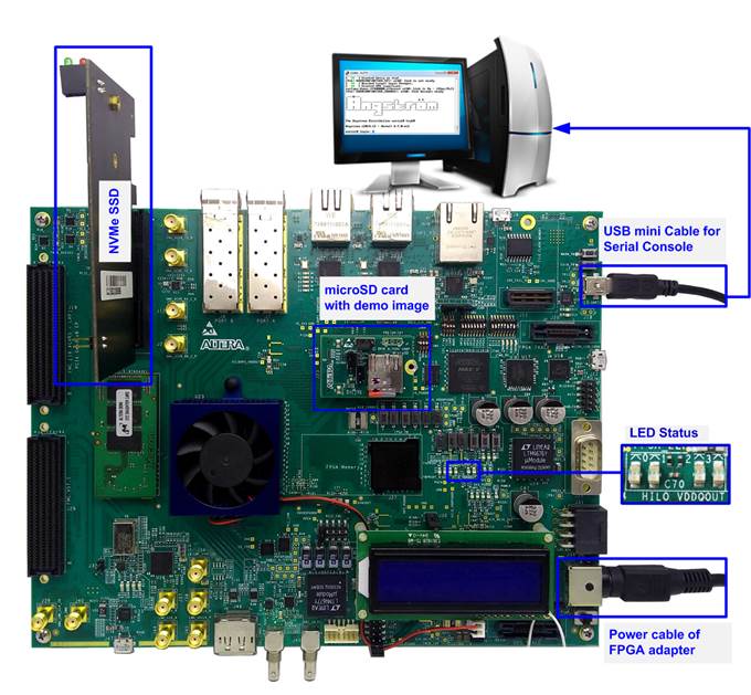
Figure 1‑1 NVMe-IP Linux Demo on Arria10 SoC Development Board
2 Demo setup
2.1 Prepare demo image file to microSD Card
The sequence to prepare image file is shown as follows.
1) Extract “sd_card_image_a10.img.tar.gz” to get output file “sd_card_image_a10.img”.
2) Connect microSD card to PC by using card reader.
3) Open “Win32DiskImage” application.
4) Copy “sd_card_image_a10.img” to microSD by using Win32DiskImage, as shown in Figure 2‑1.
a. Select drive to microSD card drive.
b. Browse to directory path of “sd_card_image_a10.img” file.
c. Click “Write” to start dump data.
d. “Confirm overwrite” window is displayed. Click “Yes” to confirm data dump.
e. Wait until progress status updated from 0% to 100%. “Complete” window with “Write Successful” is displayed. Click “OK” to complete this step.
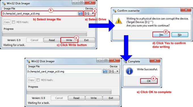
Figure 2‑1 Write demo image file to microSD Card
2.2 PCIe setup and Board setup
1) Power off system.
2) Insert microSD card to the socket on daughter cards.
3) Connect NVMe SSD to PCIe connector on FPGA board, as shown in Figure 2‑2.
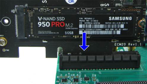
Figure 2‑2 NVMe SSD connection on FPGA board
4) Connect mini USB cable from FPGA board to PC for Serial console, as shown in Figure 2‑3.
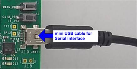
Figure 2‑3 USB cable connection
5) Set SW3[1] /[2]/ [6]/ [8] = OFF position to enable JTAG of HPS, FPGA, and MAX, as shown in Figure 2‑4.
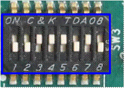
Figure 2‑4 JTAG Enable for Arria10 SoC board
6) Connect FPGA power adapter to FPGA board, as shown in Figure 2‑5.
7) Power on FPGA development board.
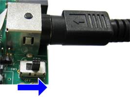
Figure 2‑5 Power on FPGA board
8) Open Serial console software such as HyperTerminal. Software setting is BaudRate=115,200, Data=8 bit, Non-Parity, and Stop=1.
9) On PC Serial console, please wait Linux boot-up until login required, as shown in Figure 2‑6.
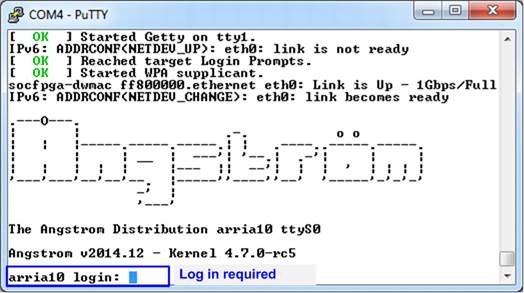
Figure 2‑6 Linux Boot-up
10) Check LED status on FPGA board. The description of LED is shown as follows.
Table 1 LED Definition
|
GPIO LED |
ON |
OFF |
|
0 |
Normal operation |
System is in reset condition |
|
1 |
System is busy |
Idle status |
|
2 |
Error detect |
Normal operation |
|
3 |
Data verification fail |
Normal operation |
Figure 2‑7 4-bit LED Status for user output
11) After programming completely, LED[0] and LED[1] are ON which mean that PCIe initialization is processing. Then, LED[1] is OFF to show that PCIe completes initialization process and system is ready to receive command from user.
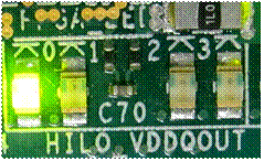
Figure 2‑8 LED status after program configuration file and PCIe initialization complete
3 Test Menu
Before running the test application, user must login to Linux system by login name as “root”, as shown in Figure 3‑1.
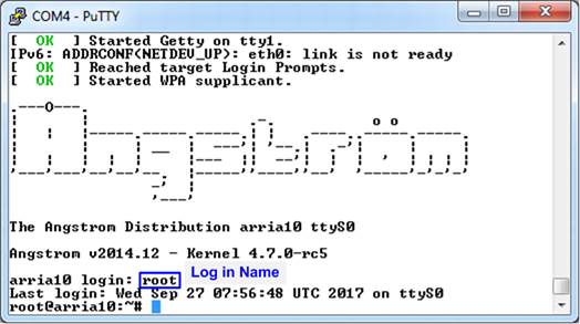
Figure 3‑1 Login to Linux system
Next, insert module and running test application by typing following command.
>> insmod dg_universal.ko
>> ./dg_universal/application/dguTestApp
After that, main menu is displayed on Serial console, as shown in Figure 3‑2.
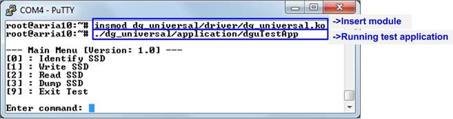
Figure 3‑2 Insert module and running test application
3.1 Identify Device
Select ‘0’ to send Identify command to NVMe SSD. When operation is completed, SSD capacity and model name are displayed on the console.
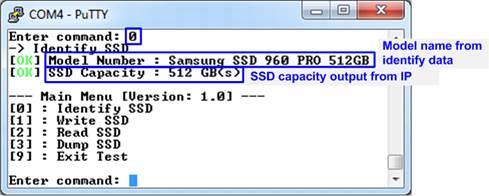
Figure 3‑3 Result from Identify Device menu
3.2 Write SSD
Select ‘1’ to send Write command to NVMe SSD. Three inputs are required for this menu.
1) Start LBA: Input start address of SSD in sector unit. The input is decimal unit when input only digit number. User can add “0x” to be prefix when input is hexadecimal unit.
2) Sector Count: Input total transfer size in sector unit. The input is decimal unit when input only digit number. User can add “0x” to be prefix when input is hexadecimal unit.
3) Test pattern: Select test pattern of test data for writing to SSD. Five types can be selected, i.e. 32-bit increment, 32-bit decrement, all 0, all 1, and 32-bit LFSR counter.
As shown in Figure 3‑4, if all inputs are valid, the operation will be started. During writing data, current transfer size is displayed on the console to show that system still run. Finally, test performance, total size, and total time usage are displayed on the console as test result.
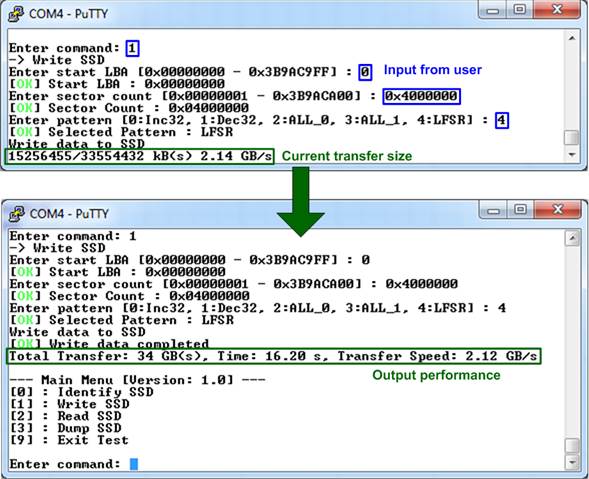
Figure 3‑4 Input and result of Write SSD menu
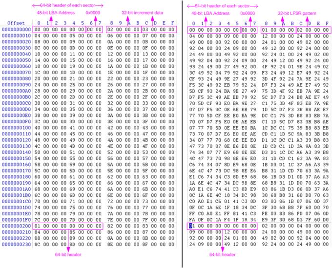
Figure 3‑5 Example Test data in sector#0/#1 by increment/LFSR pattern
Test data of each sector has different 64-bit header which consists of 48-bit LBA address and 16-bit all 0 value. 48-bit LBA address is unique value for each sector. After that, the test pattern is filled following user selection such as 32-bit increment pattern (left window of Figure 3‑5), 32-bit LFSR pattern (right window of Figure 3‑5).
Figure 3‑6 – Figure 3‑8 shows error message when user input is invalid. “Input is not in range” is displayed on the console. Then, it returns to main menu to receive new command.
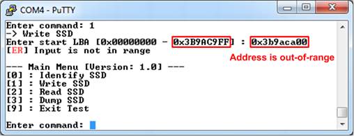
Figure 3‑6 Invalid Start LBA input
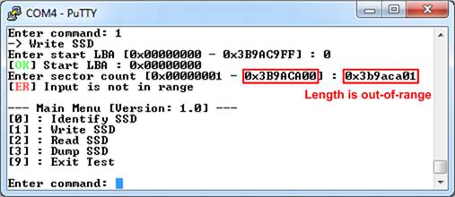
Figure 3‑7 Invalid Sector count input
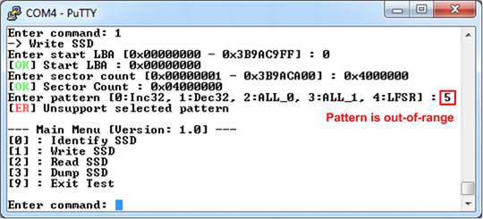
Figure 3‑8 Invalid Test pattern input
3.3 Read SSD
Select ‘2’ to send Read command to NVMe SSD. Three inputs are required for this menu.
1) Start LBA: Input start address of SSD in sector unit. The input is decimal unit when input only digit number. User can add “0x” to be prefix when input is hexadecimal unit.
2) Sector Count: Input total transfer size in sector unit. The input is decimal unit when input only digit number. User can add “0x” to be prefix when input is hexadecimal unit.
3) Test pattern: Select test pattern to verify data from SSD. Test pattern must be matched with the test pattern which is used during write test. Five types can be selected, i.e. 32-bit increment, 32-bit decrement, all 0, all 1, and 32-bit LFSR counter.
Similar to write test if all inputs are valid, test system will read data from SSD. Test performance, total size, and total time usage are displayed after end of transfer. “Invalid input” will be displayed if some input values are out-of-range.
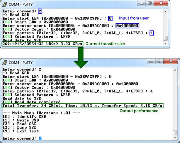
Figure 3‑9 Input and result of Read SSD menu
Figure 3‑10 shows the error message when data verification is failed. “verification fail” is displayed with Read data and Expected data. User must wait until the test is completed.
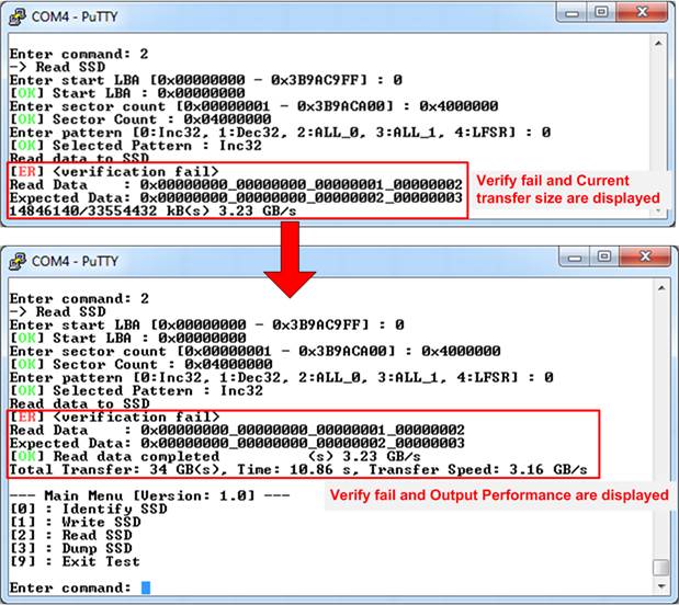
Figure 3‑10 Data verification is failed
3.4 Dump SSD
Select ‘3’ to send Dump command to NVMe SSD. Only one input is required for this menu.
Start LBA: Input start address of SSD in sector unit. The input is decimal unit when input only digit number. User can add “0x” to be prefix when input is hexadecimal unit.
Similar to write and read test if the input is valid, test system will return data 1 sector (512 byte) from SSD.
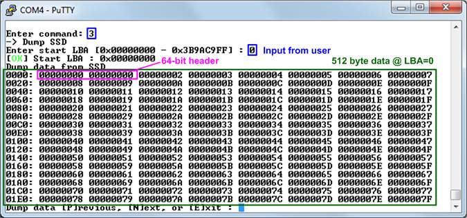
Figure 3‑11 Dump menu example
After displaying one data sector, another input is required.
Input ‘p’ to display the previous sector of Start LBA.
Input ‘n’ to display the next sector of Start LBA.
Input ‘e’ to go back to main menu.
As shown in Figure 3‑12, when input ‘n’ to show the data of the next sector, Start LBA is increased by 1 (from 0 to 1).
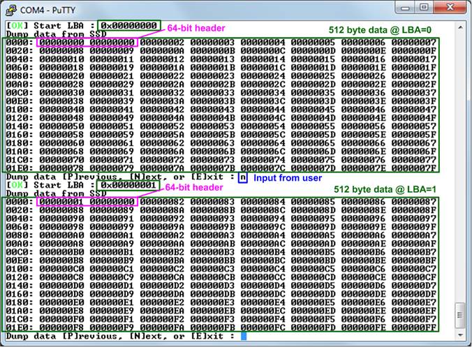
Figure 3‑12 Example of Dump menu when input 'n'
As shown in Figure 3‑13, when input ‘p’ to show the data of the previous sector, Start LBA is decreased by 1 (from 1 to 0).

Figure 3‑13 Example of Dump menu when input 'p'
Main menu is displayed when user input ‘e’ to exit Dump menu, as shown in Figure 3‑14.
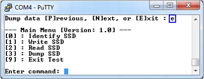
Figure 3‑14 Exit Dump SSD menu
3.5 Exit Test
Select ‘9’ to exit test application.
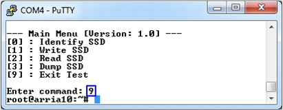
Figure 3‑15 Exit test application
4 Revision History
|
Revision |
Date |
Description |
|
1.0 |
19-Feb-18 |
Initial version release |