1 Introduction
To design the hardware in FPGA, there are many design solutions for user application. First solution is using pure hardware logic without OS like NVMe-IP reference design (as shown in the left side of Figure 1‑1). System without OS, the design uses less FPGA resources, suitable for simple design. User controls hardware system through hardware interfaces such as DIPSW or small CPU like NiosII which running the firmware as Baremetal OS to process user command.
Second solution is using hardware logic with OS like this reference design (as shown in the right side of Figure 1‑1). Using OS consumes FPGA resources more than the first solution, but the benefit of OS is suitable for complicated system and various applications. To connect hardware to OS, device driver needs to be used as media to write/read register to control hardware. Special character device driver is created for the ease of use by Application layer to access hardware.
Comparing to NVMe-IP reference design, the hardware on Linux reference design has additional feature to allow CPU to read the latest data output from NVMe-IP for Read command. CPU uses character device driver to read the data, so one data word is returned to CPU for each access. This hardware is suitable for system monitoring which does not require high performance transfer.
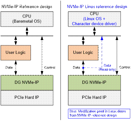
Figure 1‑1 Comparison between NVMe-IP reference design and Linux reference design
2 Hardware
NVMe-IP Linux reference design is modified from NVMe-IP reference design to use ARM CPU with Linux OS instead of NiosII CPU with Baremetal OS. Please see more details of NVMe-IP reference design from following document.
http://www.dgway.com/products/IP/NVMe-IP/dg_nvmeip_refdesign_intel_en.pdf
http://www.dgway.com/products/IP/NVMe-IP/dg_nvmeip_instruction_intel_en.pdf
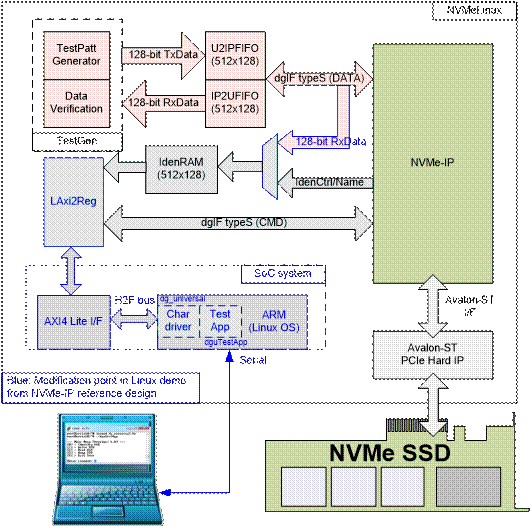
Figure 2‑1 NVMe-IP Linux reference design
Comparing to NVMe-IP reference design, the modification hardware of Linux reference design is shown in blue color of Figure 2‑1. CPU in this reference design is ARM, not NiosII. CPU interfacing with hardware is AXI4-Lite bus instead of Avalon bus to connect to H2F bus of ARM.
To support AXI4-Lite protocol, LAxi2Reg module is designed to convert the interface from AXI4-Lite to register interface. Control and data path of NVMe-IP in test system is almost similar to NVMe-IP reference design. But IdenRAM in Linux reference design is designed to store two data types, i.e. the latest data from Read command (new feature) and data from Identify command (original feature). The 1st data of Read command is stored to Addr=0 of IdenRAM and the address is increased before receiving the next data. If transfer size of Read command is more than 8 Kbyte which is IdenRAM size, new data will replace the old data in IdenRAM.
CPU in Linux reference design is ARM which runs Linux OS. Test application on OS needs to access the hardware through device driver. For simply design, character device driver is designed to allow user to access write/read register of hardware. Two softwares are designed for this reference design, i.e. “dg_universal” which is the device driver and “dguTestApp” which is the test application. User controls the system through Serial console. More details of the hardware are described as follows.
2.1 Avalon-ST PCIe Hard IP
Some FPGA models include the Hard IP for PCIe which uses Avalon stream to be user interface. The reference design uses PCIe Hard IP to implement PCIe protocol. More details of the IP can be found from following website.
https://www.altera.com/documentation/lbl1414599283601.html
2.2 NVMe-IP
NVMe-IP implements NVMe protocol to access NVMe SSD through PCIe Hard IP. User interface of NVMe-IP is designed following dgIF typeS interface. More details of the IP are described in NVMe-IP datasheet.
http://www.dgway.com/products/IP/NVMe-IP/dg_nvmeip_datasheet_intel_en.pdf
2.3 TestGen
This is the example of user logic to interface with NVMe-IP. There are two operations in TestGen, i.e. TestPatt Generator and Data Verification. TestPatt Generator is designed to generate 128-bit data to NVMe-IP in Write command while Data verification is designed to verify 128-bit data from NVMe-IP in Read command. This module is similar to the hardware in NVMe-IP reference design. More details can be found in Topic 5 of NVMe-IP reference design document.
2.4 LAxi2Reg
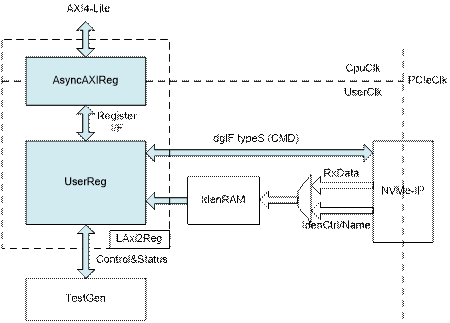
Figure 2‑2 LAxi2Reg interface
This module consists of two submodules, i.e. AsyncAXIReg and UserReg. AsyncAXIReg is designed to convert AXI4-Lite bus to be register interface and to convert clock domain from CPU clock (CpuClk) to user clock (UserClk) system.
UserReg module includes the logic to decode Write/Read address to select the register for current access. The address is decoded following Table 2‑1. Transferred parameters such as transfer direction, size, and address from user are converted to be a command interface of dgIF typeS for NVMe-IP and control signal for TestGen module. During transfer, CPU reads the register to check NVMe-IP status (CMD interface of dgIF typeS), TestGen result, Identify device data (IdenCtrl/Name), or the latest data from Read command (RxData).
Table 2‑1 Register map definition
|
Address |
Register Name |
Description |
|
Rd/Wr |
(Label in the “dg_universal.h”) |
|
|
BA+0x0000 – BA+0x00FF : Device Control |
||
|
BA+0x00 |
User Address (Low) Reg |
[31:0]: Input to be start sector address (UserAddr[31:0] of dgIF typeS) |
|
Wr |
(CTRL_DEVADRL) |
|
|
BA+0x04 |
User Address (High) Reg |
[15:0]: Input to be start sector address (UserAddr[47:32] of dgIF typeS) |
|
Wr |
(CTRL_DEVADRH) |
|
|
BA+0x08 |
User Length (Low) Reg |
[31:0]: Input to be transfer length in sector unit (UserLen[31:0] of dgIF typeS) |
|
Wr |
(CTRL_DEVLENL) |
|
|
BA+0x0C |
User Length (High) Reg |
[15:0]: Input to be transfer length in sector unit (UserLen[47:32] of dgIF typeS) |
|
Wr |
(CTRL_DEVLENH) |
|
|
BA+0x10 |
User Command Reg |
[1:0]: Input to be user command (UserCmd of dgIF typeS) “00”-Identify, “10”-Write SSD, “11”-Read SSD When this register is written, the design generates command request to NVMe-IP to start new command operation. |
|
Wr |
(CTRL_DEVCMD) |
|
|
BA+0x14 |
Test Pattern Reg |
[2:0]: Test pattern select “000”-Increment, “001”-Decrement, “010”-All 0, “011”-All 1, “100”-LFSR |
|
Wr |
(CTRL_PATTERN) |
|
|
Address |
Register Name |
Description |
|
Rd/Wr |
(Label in the “dg_universal.h”) |
|
|
BA+0x0100 – BA+0x01FF : Device Status |
||
|
BA+0x100 |
User Status Reg |
[0]: UserBusy of dgIF typeS (‘0’: Idle, ‘1’: Busy) [1]: UserError of dgIF typeS (‘0’: Normal, ‘1’: Error) [2]: Data verification fail (‘0’: Normal, ‘1’: Error) [4:3]: PCIe speed from IP (“00”: No linkup, “01”: PCIe Gen1, “10”: PCIe Gen2, “11”: PCIe Gen3) |
|
Rd |
(STAT_USRSTS) |
|
|
BA+0x104 |
Total disk size (Low) Reg |
[31:0]: Total capacity of SSD in sector unit (LBASize[31:0] of dgIF typeS) |
|
Rd |
(STAT_LBASIZEL) |
|
|
BA+0x108 |
Total disk size (High) Reg |
[15:0]: Total capacity of SSD in sector unit (LBASize[47:32] of dgIF typeS) |
|
Rd |
(STAT_LBASIZEH) |
|
|
BA+0x10C |
User Error Type Reg |
[31:0]: User error status (UserErrorType[31:0] of dgIF typeS) |
|
Rd |
(STAT_USRERRTYPE) |
|
|
BA+0x114 |
Completion Status Reg |
[15:0]: Status from Admin completion (AdmCompStatus[15:0] from NVMe-IP) [31:16]: Status from IO completion (IOCompStatus[15:0] from NVMe-IP) |
|
Rd |
(STAT_COMPSTS) |
|
|
BA+0x118 |
NVMe CAP Reg |
[31:0]: NVMeCAPReg[31:0] output from NVMe-IP |
|
Rd |
(STAT_NVMCAP) |
|
|
BA+0x11C |
NVMe IP Test pin Reg |
[31:0]: TestPin[31:0] output from NVMe-IP |
|
Rd |
(STAT_NVMTTESTPIN) |
|
|
BA+0x120 |
Data Failure Address (Low) Reg |
[31:0]: Latch value of failure address[31:0] in byte unit from read command |
|
Rd |
(STAT_RDFAILNOL) |
|
|
BA+0x124 |
Data Failure Address (High) Reg |
[24:0]: Latch value of failure address [56:32] in byte unit from read command |
|
Rd |
(STAT_RDFAILNOH) |
|
|
BA+0x130 |
Expected value Word0 Reg |
[31:0]: Latch value of expected data [31:0] from read command |
|
Rd |
(STAT_EXPPATW0) |
|
|
BA+0x134 |
Expected value Word1 Reg |
[31:0]: Latch value of expected data [63:32] from read command |
|
Rd |
(STAT_EXPPATW1) |
|
|
BA+0x138 |
Expected value Word2 Reg |
[31:0]: Latch value of expected data [95:64] from read command |
|
Rd |
(STAT_EXPPATW2) |
|
|
BA+0x13C |
Expected value Word3 Reg |
[31:0]: Latch value of expected data [127:96] from read command |
|
Rd |
(STAT_EXPPATW3) |
|
|
BA+0x140 |
Read value Word0 Reg |
[31:0]: Latch value of read data [31:0] from read command |
|
Rd |
(STAT_RDPATW0) |
|
|
BA+0x144 |
Read value Word1 Reg |
[31:0]: Latch value of read data [63:32] from read command |
|
Rd |
(STAT_RDPATW1) |
|
|
BA+0x148 |
Read value Word2 Reg |
[31:0]: Latch value of read data [95:64] from read command |
|
Rd |
(STAT_RDPATW2) |
|
|
BA+0x14C |
Read value Word3 Reg |
[31:0]: Latch value of read data [127:96] from read command |
|
Rd |
(STAT_RDPATW3) |
|
|
BA+0x150 |
Current test byte (Low) Reg |
[31:0]: Current test data size of TestGen module in byte unit (bit[31:0]) |
|
Rd |
(STAT_CURTESTSIZEL) |
|
|
BA+0x154 |
Current test byte (High) Reg |
[24:0]: Current test data size of TestGen module in byte unit (bit[56:32]) |
|
Rd |
(STAT_CURTESTSIZEH) |
|
|
BA+0x2000 : Device Identification Data |
||
|
BA+0x2000 – 0x3FFF |
IdenRAM area (IDEN_CTRL) |
8Kbyte Identify Controller/Namespace data or the latest data from Read command |
Note: BA is base address of LAxi2Reg which is mapped to H2F bus of ARM.
3 Software
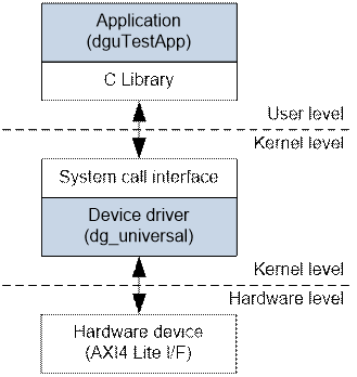
Figure 3‑1 Software on ARM in reference design
Figure 3‑1 shows software structure of the demo in reference design. Two softwares for Linux OS are specially designed to interface with the hardware, i.e. “dg_universal” which is character device driver and “dguTestApp” which is test application.
Memory map shown in Table 2‑1 has been declared in the device driver. The sequence to write/read hardware register for each operation is designed in the device driver. The test application is designed to interface with user to get the parameters and the operation request. After verifying user input, the application calls the function to write, read, or identify the device. Otherwise, the application shows the hardware status during operation. Transfer performance as a test result is shown when completes the operation. More details of the software are described as follows.
3.1 Device driver (dg_universal)
The device driver in reference design is designed to write/read hardware registers for sending control signals and monitoring status signals. Test data transferring with SSD is generated and verified by the hardware, not by CPU. So, it does not need to use block device driver to manage data flow by CPU. Using character device driver is simple and fit for this system.
There are many functions in the device driver. This document describes some functions which the operation is related to the hardware in NVMe-IP Linux reference design.
3.1.1 dgu_readIden
This function is called to read device model name and device capacity from Identify command. The sequence of the function is shown as follows.
1) Clear value in temp buffer.
2) Read device model name from IdenRAM (at IDEN_CTRL address) to store to temp buffer.
3) Read device capacity from STAT_LBASIZE register and convert to Gigabyte unit.
4) Store device capacity to temp buffer.
5) Return data in the temp buffer.
3.1.2 dgu_readError
This function is called when error is found. Error type is decoded in this function. The sequence of the function is shown as follows.
1) Read error type value from STAT_USERRTYPE register.
2) Decode error value starting from the lowest bit of STAT_USERRTYPE register and return the error message following the error type. For example, “PCIe Class Code Error” is returned when bit0 of STAT_USERRTYPE is asserted to ‘1’.
3.1.3 dgu_read
This function is called to check the status of current operation. The sequence of the function depends on the operation.
a) For Identify operation,
1) Check UserBusy flag (bit0 of STAT_USRSTS). Exit the program and return 0 when UserBusy still be equal to ‘1’.
2) Check UserError flag (bit1 of STAT_USRSTS). Exit the program and return error when UserError is set to ‘1’.
3) If no flag is detected, the function will call dgu_readIden function to read device model name and capacity.
b) For Write and Read operation,
1) Check UserError flag (bit1 of STAT_USRSTS). If UserError is set to ‘1’, dgu_readError function will be called to decode error message.
2) Check Verification fail flag (bit2 of STAT_USRSTS). If flag is set to ‘1’, Read value (STAT_RDPATW0-W3) and Expected value (STAT_EXPPATW0-W3) will be returned.
3) Check UserBusy flag (bit0 of STAT_USRSTS). If UserBusy is set to ‘1’, current transfer size in Kbyte unit will be returned.
4) If no flag is detected, the function will return END status.
c) For Dump operation,
1) Check UserBusy flag (bit0 of STAT_USRSTS). If UserBusy is set to ‘1’, the function will return BUSY status.
2) Check Verification fail flag (bit2 of STAT_USRSTS). If flag is set to ‘1’, the function will return ERROR status and call dgu_readError function to decode error message.
3) If no flag is detected, the function will return the data from IdenRAM which stores the latest data from Read command.
3.1.4 dgu_ioctrl
This function is called to write hardware registers to start the operation. Similar to dgu_read function, the sequence of the function depends on the operation.
a) For Identify operation,
1) Set CTRL_DEVCMD register = Identify command.
b) For Write and Read operation,
1) Receive parameters from the user.
2) Set CTRL_DEVADR register = start sector address from user.
3) Set CTRL_DEVLEN register = total sector length from user.
4) Set CTRL_PATTERN register following user input.
5) Set CTRL_DEVCMD register = Write or Read command.
c) For Dump operation,
1) Receive parameters from the user.
2) Set CTRL_DEVADR register = start sector address from user.
3) Set CTRL_DEVLEN register = total sector length from user.
4) Set CTRL_DEVCMD register = Read command.
3.2 Test application (dguTestapp)
There are four operations for user to run the demo, i.e. Identify SSD to read SSD information, Write SSD to check write performance, Read SSD to check read performance and verify test data, and Dump SSD to monitor the data in SSD. More details of each operation are described as follows.
3.2.1 Identify SSD
This menu is created to read data from Identify command which is stored in IdenRAM. The sequence of Identify SSD is shown as follows.
1) Read Identify data from IdenRAM and store in the buffer.
2) Clear model_name and model_size variable.
3) Copy model name from Identify data to model_name variable.
4) Copy SSD capacity to model_size variable.
5) Print out model_name and model_size.
3.2.2 Write SSD
This menu is created to send write command to SSD. Three inputs are required to set Start LBA, Sector count, and Pattern. The operation will be cancelled if input is invalid. The sequence of Write SSD is shown as follows.
1) Receive Start LBA, Sector count, and Pattern from user.
2) Write Start LBA, Sector count, and Pattern to registers in NVMe-IP.
3) Read status of NVMe-IP.
4) Check busy status of NVMe-IP.
5) Print current transfer size.
6) Sleep for 100 usec.
7) Run step 3) - 6) in the loop until NVMe-IP is idle.
8) Go back to main menu.
3.2.3 Read SSD
This menu is created to send read command to SSD. Three inputs are required, as same as Write SSD, to set Start LBA, Sector count, and Pattern. The operation will be cancelled if input is invalid. The sequence of Write SSD is shown as follows.
1) Receive Start LBA, Sector count, and Pattern from user.
2) Write Start LBA, Sector count, and Pattern to registers in NVMe-IP.
3) Read status of NVMe-IP.
4) Read data verification status
5) Check busy status of NVMe-IP.
6) Print current transfer size.
7) Sleep for 100 usec.
8) Run step 3) - 8) in the loop until NVMe-IP is idle.
9) Go back to main menu.
3.2.4 Dump SSD
This menu is created to send read command to SSD. Only one input is required to set Start LBA. The operation will be cancelled if input is invalid. One sector data is shown on the console. Next, another input is required from user. There are three options for user selection, i.e. displaying the next sector, displaying previous sector, or exit to main menu. The sequence of Dump SSD is shown as follows.
1) Receive Start LBA from user.
2) Check whether Start LBA is valid or not.
3) Send read data one sector
4) Print out data one sector
5) Required input from user.
6) Select 3 options
· Previous : show the previous sector and run step 3) – 5)
· Next : show the next sector and run step 3) – 5)
· Exit : exit to main menu
4 Revision History
|
Revision |
Date |
Description |
|
1.0 |
15-Feb-18 |
Initial version release |