1 Environment Requirement
To run the demo on FPGA development board, please prepare following environment.
1) FPGA Development board: VCU118
2) PC installing Xilinx programmer software (Vivado) and Serial console software such as TeraTerm.
3) AB18-PCIeX16 board + ATX power supply for AB18.
4) Xilinx power adapter for FPGA board
5) ASROCK Ultra Quad M.2 Card, connecting B side (Device) of AB18.
https://www.asrock.com/mb/spec/product.asp?Model=ULTRA QUAD M.2 CARD
6) Four M.2 NVMe SSDs.
7) Two micro USB cables for programming FPGA and Serial console, connecting between FPGA board and PC
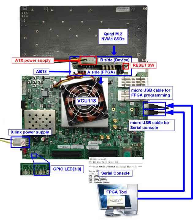
Figure 1‑1 NVMe-IP RAID0 demo setup by AB18 on VCU118
2 Demo setup
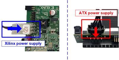
Figure 2‑1 Power supply connection
2) Connect four M.2 NVMe SSDs to four connectors on Ultra Quad M.2 Card as shown in Figure 2‑2.
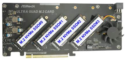
Figure 2‑2 Four M.2 NVMe SSDs with Ultra Quad M.2 Card
3) Confirm that two mini jumpers are inserted at J5 connector on AB18. After that, connect FPGA Side (A-side) on AB18 to PCIe connector on FPGA board and connect Quad M.2 NVMe SSD Card to device side (B-Side) on AB18, as shown in Figure 2‑3.
Warning: Please confirm that the Quad M.2 NVMe SSD is inserted in the correct side of AB18 (B-side, not A-side) before power on system.
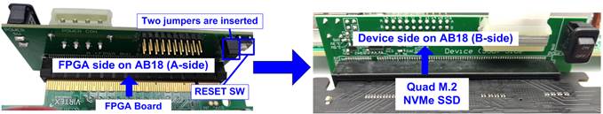
Figure 2‑3 Connect Adapter board to Quad M.2 NVMe SSD Card and FPGA board
4) Connect two micro USB cables between FPGA board and PC for FPGA programming and Serial console.

Figure 2‑4 USB cable connection
5) Power on FPGA development board, ATX power supply for AB18, and AB18 board, as shown in Figure 2‑5.
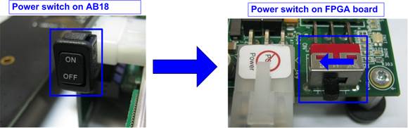
Figure 2‑5 Turn on power switch on FPGA and adapter board
6) On PC, additional COM port is detected after connecting USB cables to FPGA board. More than one COM ports are detected.
In case of VCU118, select Standard COM port as shown in Figure 2‑6.
On Serial console, the setting is as follows.
Baud rate=115,200, Data=8-bit, Non-Parity, and Stop = 1.
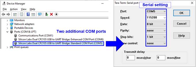
Figure 2‑6 Two COM ports from FPGA connection
7) Use Vivado tool to download configuration file, as shown in Figure 2‑7.
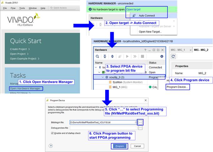
Figure 2‑7 Programmed by Vivado
8) Check LED status on FPGA board. The description of LED is as follows.
Table 2‑1 LED Definition
|
GPIO LED |
ON |
OFF |
|
0 |
Normal operation |
SSD is not good status |
|
1 |
System is busy |
Idle status |
|
2 |
IP Error detect |
Normal operation |
|
3 |
Data verification fail |
Normal operation |
9) After programming completely, LED[0] and LED[1] are ON during PCIe initialization process. Then, LED[1] changes to OFF after PCIe completes initialization process.
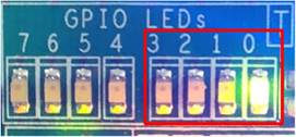
Figure 2‑8 LED status after programming configuration file and finishing PCIe initialization
10) On the console, the message is displayed to show current status as follows.
“Waiting PCIe Linkup” is displayed after finishing configuration.
“Waiting IP initialization” is displayed after PCIe is linked up.
PCIe speed and number of PCIe lanes are displayed, after RAID0 finishes initialization. Finally, main menu to run six commands is shown on the console.
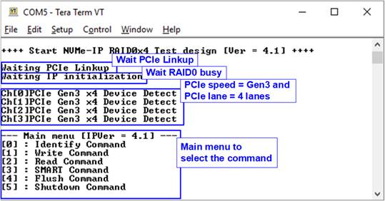
Figure 2‑9 Main menu after RAID0 finishes initialization
When LBA size is 4 Kbyte, the error message is displayed on the console as shown in Figure 2‑10

Figure 2‑10 Error message when LBA does not support
3 Test Menu
3.1 Identify Command
Select ‘0’ to send Identify command to RAID0.
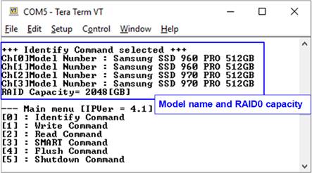
Figure 3‑1 Test result when running Identify command
After finishing the operation, the SSD information output from Identify command is displayed. The console shows two values.
1) SSD model number: This value is decoded from Identify controller data.
2) RAID capacity: This value is calculated by multiplying device capacity in channel#0 by 4.
3.2 Write Command
Select ‘1’ to send Write command to RAID0.
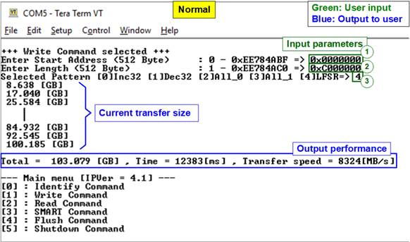
Figure 3‑2 Test result when running Write command
User sets three parameters as follows.
1) Start Address: Start address to write RAID0 as 512-byte unit. The input is decimal unit when the input is only digit number. User can add “0x” to be a prefix for hexadecimal unit.
2) Transfer Length: Total transfer size as 512-byte unit. The input is decimal unit when the input is only digit number. User can add “0x” to be a prefix for hexadecimal unit.
3) Test pattern: Select test data pattern for writing RAID0. There are five patterns, i.e. 32-bit increment, 32-bit decrement, all 0, all 1, and 32-bit LFSR counter.
When all inputs are valid, the operation begins. During writing data, current transfer size is displayed on the console every second to show that system is still alive. Finally, total size, total time usage, and test speed are calculated and displayed on the console to be a test result.
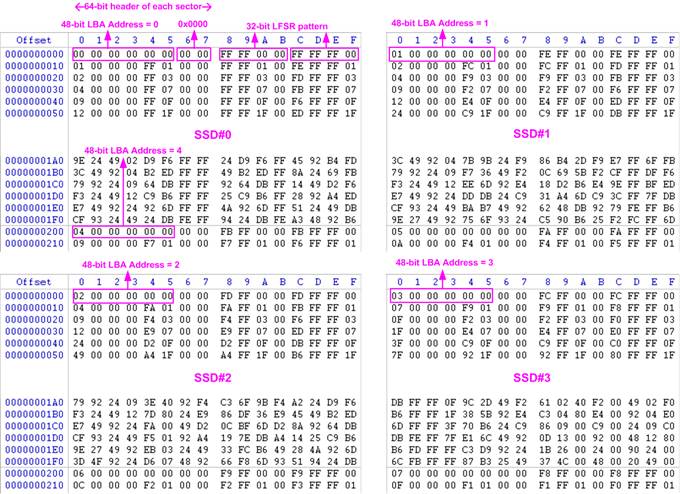
Figure 3‑3 Example Test data of the 1st and 2nd 512 byte of each SSD by using LFSR pattern
The stripe size in 4-ch RAID0 demo is 512-byte. For incremental, decremental, or LFSR pattern, each 512-byte data has unique 64-bit header which consists of 48-bit address (in 512-byte unit) and 16-bit zero value. The data after 64 bits header is the test pattern which is selected by user. The 1st stripe is mapped to the first 512-byte of SSD#0. The 2nd - the 4th stripe are mapped to the first 512-byte of SSD#1 - SSD#3 respectively, as shown in Figure 3‑3. The unique header is not included when running all-0 or all-1 pattern.
Figure 3‑4 shows the example when the input is not in the recommended range for each parameter. The console displays “Invalid input” and then the operation is cancelled.

Figure 3‑4 Error message from the invalid input
3.3 Read Command
Select ‘2’ to send Read command to RAID0.
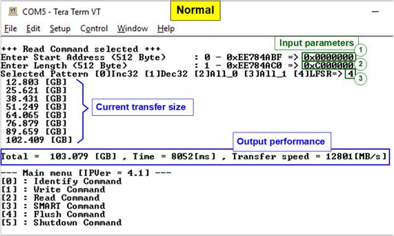
Figure 3‑5 Input and result of Read Command menu
User inputs three parameters as follows.
1) Start Address: Start address to read SSD as 512-byte unit. The input is decimal unit when the input is only digit number. User can add “0x” to be a prefix for hexadecimal unit.
2) Transfer Length: Total transfer size as 512-byte unit. The input is decimal unit when the input is only digit number. User can add “0x” as a prefix for hexadecimal unit
3) Test pattern: Select test data pattern to verify data from RAID0. Test pattern must be matched with the pattern using in Write Command menu. There are five patterns, i.e. 32-bit increment, 32-bit decrement, all 0, all 1, and 32-bit LFSR counter
Similar to Write command menu, test system starts reading data from RAID0 when all inputs are valid. During reading data, current transfer size is displayed on the console every second to show that system is still alive. Total size, total time usage, and test speed are calculated and displayed after finishing data transferring.
Figure 3‑6 shows error message when data verification is failed. “Verify fail” is displayed with the information of the 1st failure data, i.e. the error byte address, the expected value, and the read value. User presses any keys to cancel read operation or waits until finishing Read command. Without cancelling the operation, the output performance is displayed on the console after finishing the operation.
When pressing some keys to cancel the operation, the read command does not complete in the good sequence. It is recommended to power-off/on AB18 and then presses “RESET” button to restart system.
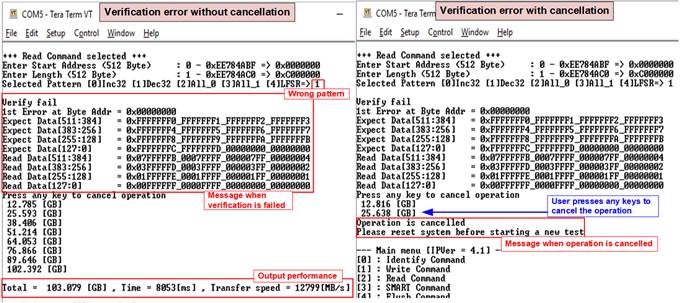
Figure 3‑6 Data verification is failed
3.4 SMART Command
Select ‘3’ to send SMART command to RAID0.
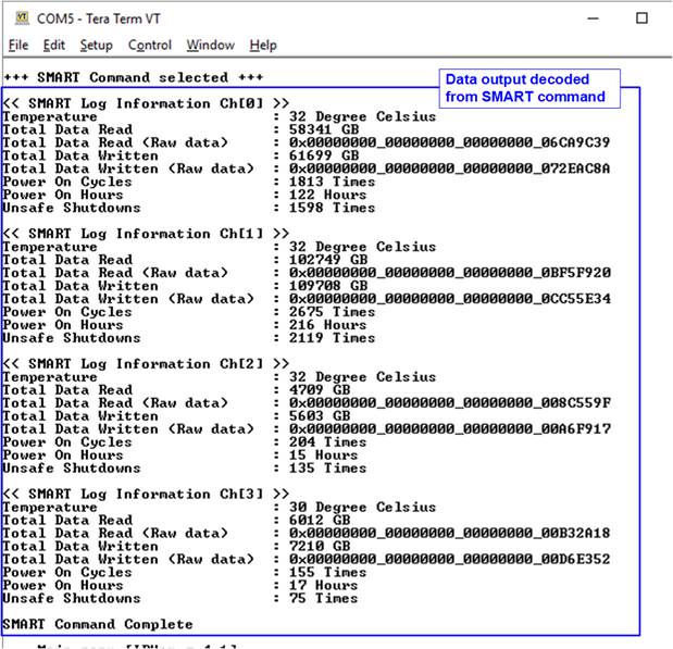
Figure 3‑7 Test result when running SMART command
When the operation is completed, SMART/Health Information (output from SMART command) is displayed as shown in Figure 3‑7. The console shows six values from each SSD.
1) Temperature in °C unit.
2) Total Data Read decoded as GB/TB unit. Also, raw data without decoding is displayed in 128-bit hexadecimal unit. The unit size of raw data is 512,000 byte.
3) Total Data Written decoded as GB/TB unit. Also, raw data without decoding is displayed in 128-bit hexadecimal unit. The unit size of raw data is 512,000 byte.
4) Power On Cycles: Display the number of power cycles.
5) Power On Hours: Display period of time in hours that the SSD is power on.
6) Unsafe Shutdowns: Display the number of unsafe shutdowns of SSD
3.5 Flush Command
Select ‘4’ to send Flush command to RAID0.
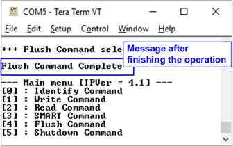
Figure 3‑8 Test result when running Flush command
“Flush Command Complete” is displayed after finishing Flush operation.
3.6 Shutdown Command
Select ‘5’ to send Shutdown command to RAID0.

Figure 3‑9 Message after Shutdown command is completed
The confirmation message is displayed on the console. User enters ‘y’ or ‘Y’ to confirm the operation or enters other keys to cancel the operation.
After finishing Shutdown operation, “Shutdown command is complete” is displayed on the console as the last message. Main menu is not displayed and user needs to power off/on the test system to start new test operation.
4 Revision History
|
Revision |
Date |
Description |
|
1.0 |
13-Nov-19 |
Initial version release |
|
1.1 |
20-Apr-20 |
Remove power adapter cable from AB18 |