4-ch RAID0 Design (NVMe-IP) reference design manual
Rev1.1 11-Aug-23
2.2.2 Integrated Block for PCIe
3.1 Test firmware (nvmeipraid0x4test.c)
3.2 Function list in Test firmware
1 Introduction
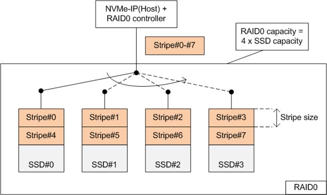
Figure 1‑1 RAID0 by 4 SSDs data format
RAID0 system uses multiple storages to extend total storage capacity and increase write/read performance. Assumed that total number of devices connecting in RAID0 system is N, total storage capacity of RAID0 is equal to N times of one device capacity. Write and read performance of RAID0 are almost equal to N times of one device performance.
Data format of RAID0 is shown in Figure 1‑1. Data stream of the host side is split into a small stripe for transferring with one SSD at a time. Stripe size is the data size transferring with one SSD before switching to other SSDs. In RAID0 reference design, stripe size is equal to 512-byte.
In this demo, four SSDs is connected in the system. It is recommended to use the same model of SSD for all channels to match the characteristic and achieve the best performance. As a result, the total capacity is equal to four times of one SSD and the write/read performance are almost four times of one SSD performance.
The demo uses FIFO implemented by BlockRAM to be the buffer which has smaller size than DDR. Therefore, the buffer is sometimes not ready to transfer data when SSD pauses data transmission for long time in Write process. Test performance in the demo is average speed, not sustain rate. User can modify RAID0 reference design by increasing the numbers of SSD to achieve the better performance and the bigger capacity. Furthermore, user can add DDR to be data buffer in the system for supporting high-speed transferring as sustain rate.
Before running the reference design, it is recommended to study NVMe-IP datasheet and single channel demo firstly from following link.
http://www.dgway.com/products/IP/NVMe-IP/dg_nvme_ip_data_sheet_en.pdf
http://www.dgway.com/products/IP/NVMe-IP/dg_nvmeip_refdesign_en.pdf
http://www.dgway.com/products/IP/NVMe-IP/dg_nvmeip_instruction_en.pdf
2 Hardware overview
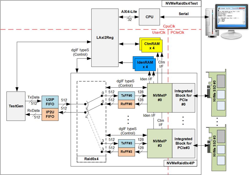
Figure 2‑1 RAID0x4 demo system by using NVMe-IP
The hardware system can be split into three groups, i.e., TestGen, NVMeRaid0x4-IP, and CPU. First, TestGen is the test logic to generate and verify test data stream with NVMeRaid0x4-IP through U2IPFIFO/IP2UFIFO. Second, NVMeRaid0x4-IP consists of the RAID0x4, four NVMe-IPs, and four PCIe hard IPs (Integrated Block for PCI Express). Data format in four NVMe SSDs is arranged as RAID0 format by RAID0x4 module. Each NVMe SSD must directly connect to one PCIe hard IP without PCIe switch. Last, CPU and LAxi2Reg are designed to interface with user through Serial interface. User can set test parameters and monitor hardware status through Serial console. After receiving the command from user, CPU firmware calculates all parameters for setting to each hardware to begin the command operation.
There are three clock domains displayed in Figure 2‑1, i.e., CpuClk, PCIeClk, and UserClk. First, CpuClk is the clock domain of CPU and its peripherals. This clock must be stable clock which can be different from the clock for other hardwares. Second, PCIeClk is the clock output from PCIe hard IP to synchronous with 128-bit AXI4 stream bus. When the PCIe hard IP is set to 4-lane PCIe Gen3, PCIeClk frequency is equal to 250 MHz. Last, UserClk is the example user clock for running all user logics such as RAID0x4, NVMe-IP, RAM, FIFO, and TestGen. According to NVMe-IP datasheet, clock frequency of UserClk must be more than or equal to PCIeClk. In this reference design, UserClk is equal to 280 MHz for PCIe Gen3.
There are six memories implemented by BlockRAM in the test system, i.e., CtmRAM, IdenRAM, TxFIFO, RxFIFO, U2IPFIFO, and IP2UFIFO.
CtmRAM stores returned data of each SSD from SMART command while IdenRAM stores returned data from Identify command. When running SMART command or Identify command, the returned data from the command is decoded by CPU which is read through LAxi2Reg module by using AXI4-Lite interface.
TxFIFO and RxFIFO are connected between RAID0x4 and NVMe-IP to convert data bus size from 512-bit to 128-bit. U2IPFIFO and IP2UFIFO are connected between TestGen and NVMeRaid0x4-IP for transferring data when running Write command and Read command respectively. TestGen is designed to monitor flow control signal of U2IPFIFO and IP2UFIFO to be always read and write data when the FIFO is ready. The FIFO depth is set to 512 x 512 bit. More details of the hardware are described as follows.
2.1 TestGen
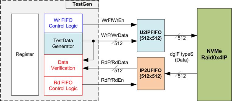
Figure 2‑2 TestGen interface
TestGen module is the test logic to send test data to NVMeRaid0x4-IP through U2IPFIFO when operating Write command. On the other hand, the test data is applied to be the expected value to verify the read data from NVMeRaid0x4-IP through IP2UFIFO when operating Read command. Control logic asserts Write enable and Read enable to �1� when the FIFOs are ready. Data bandwidth of TestGen is matched to NVMeRaid0x4-IP by running at the same clock and using the same data bus size. Therefore, NVMeRaid0x4-IP can transfer data with U2IPFIFO and IP2UFIFO without waiting data ready. The test logic can show the best performance to write and read data with the SSD through NVMeRaid0x4-IP.
Register file in the TestGen receives test parameters from user, i.e., total transfer size, transfer direction, verification enable, and test pattern selector. To control transfer size, the counter counts total test data. The details of hardware logic within TestGen module are shown in Figure 2‑3.

Figure 2‑3 TestGen hardware
As shown in the right side of Figure 2‑3, flow control signals of FIFO are WrFfAFull and RdFfEmpty. When FIFO is almost full during write operation (WrFfAFull=�1�), WrFfWrEn is de-asserted to �0� to pause data sending to FIFO. For read operation, when FIFO has data (RdFfEmpty=�0�), the logic reads data from FIFO to compare with the expected data by asserting RdFfRdEn to �1�.
The logic in the left side of Figure 2‑3 is designed to count transfer size (rDataCnt). When total data count is equal to the end size (rEndSize), set by user, write enable or read enable of FIFO is de-asserted to �0�.
The lower side of Figure 2‑3 shows the details to generate test data for writing to FIFO or verifying data from FIFO. There are five patterns to generate, i.e., all-zero, all-one, 32-bit incremental pattern, 32-bit decremental pattern, and LFSR counter, selected by Pattern Selector. The 32-bit incremental data is designed by using 51-bit counter while the decremental data is designed by connecting NOT logic to incremental data. The LFSR pattern is designed by using LFSR counter. The equation of LFSR is x^31 + x^21 + x + 1.
To implement 512-bit LFSR pattern, the data is split to be four sets of 128-bit data which uses the different start value. 128-bit data uses look-ahead technique to calculate four 32-bit LFSR data in one clock cycle. As shown Figure 2‑4, the start value of each LFSR set is designed by using combination signal of 32-bit LBA address and NOT logic of LBA address (LBAAddrB means NOT logic of LBAAddr signal).
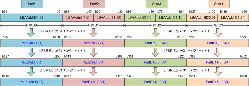
Figure 2‑4 512-bit LFSR Pattern in TestGen
Figure 2‑5 Test pattern format in each 512-byte data for Increment/Decrement/LFSR pattern
When creating all-zero or all-one pattern, every bit of data is fixed zero or one respectively. Otherwise, test patterns are designed by separating the data to be two parts for creating the unique test data in every 512-byte data. As shown in Figure 2‑5, Dword#0 and Dword#1 of every 512-byte data are replaced by 64-bit header and the remaining words (Dword#2 � Dword#127) are the test data depending on the pattern.
64-bit header is created by using the address in 512-byte unit (rTrnAddr), output from the Address counter. The address counter loads the start value from user (TrnAddr) and then increases the value after finishing 512-byte data transferring.
Test data is fed to be write data to the FIFO or the expected data for verifying with the read data from FIFO. Fail flag is asserted to �1� when data verification is failed. The example of timing diagram to write data to FIFO is shown as follows.

Figure 2‑6 Timing diagram of Write operation in TestGen
1) WrPattStart is asserted to �1� for one clock cycle when user sets the register to start write operation. In the next clock, rWrTrans is asserted to �1� to enable the control logic for generating write enable to FIFO.
2) Write enable to FIFO (rWrFfWrEn) is asserted to �1� when two conditions are met. First, rWrTrans must be asserted to �1� during the write operation being active. Second, the FIFO must not be full by monitoring WrFfAFull=�0�.
3) The write enable is also applied to be counter enable for counting total data (rDataCnt) in the write operation.
4) When FIFO is almost full (WrFfAFull=�1�), the write process is paused by de-asserting rWrFfWrEn to �0�.
5) When total data count is equal to the set value, rWrTrans is de-asserted to �0�. At the same time, rWrFfWrEn is also de-asserted to �0� to stop generating test data.
When running read operation, read enable of FIFO is only controlled by empty flag of FIFO. Data is read when FIFO has the data. It does not wait start flag for beginning the read operation and not monitor total count for stopping the read operation. When the read enable is asserted to �1�, the address counter is increased for generating the header of expect value and counting total number of read data in read operation.
2.2 NVMeRaid0x4 IP
Figure 2‑7 NVMeRaid0x4 IP hardware
Figure 2‑7 shows the example to interface NVMeRaid0x4-IP in the reference design. The user interface of NVMeRaid0x4-IP consists of control interface and data interface. The control interface receives the command parameters through dgIF typeS or custom command interface, depending on the command. Custom command interface is applied when the command is SMART command or Flush command. Otherwise, dgIF typeS is applied.
The data interface of NVMeRaid0x4 IP has four signal groups, i.e., FIFO input interface (dgIF typeS), FIFO output interface (dgIF typeS), custom command RAM interface, and Identify interface. Data bus width of FIFO interface is 512-bit while other interfaces are 128-bit. The custom command RAM interface is bi-directional interface while others are one directional interface. In the reference design, the custom command RAM interface is used to transfer data of SMART command from NVMeRaid0x4-IP to LAxi2Reg only. Another direction is not used.
2.2.1 NVMe-IP
NVMe-IP implements NVMe protocol of the host side to access one NVMe SSD directly without PCIe switch connection. NVMe-IP supports six commands, i.e., Write, Read, Identify, Shutdown, SMART, and Flush. NVMe-IP is designed to directly connect with the PCIe hard IP. More details of the NVMe-IP are described in the datasheet.
https://dgway.com/products/IP/NVMe-IP/dg_nvme_ip_data_sheet_en.pdf
2.2.2 Integrated Block for PCIe
This block is the hard IP in Xilinx device which implements Physical, Data Link, and Transaction Layers of PCIe specification. More details are described in Xilinx document.
PG213: UltraScale+ Devices Integrated Block for PCI Express
https://www.xilinx.com/support/documentation/ip_documentation/pcie4_uscale_plus/v1_3/pg213-pcie4-ultrascale-plus.pdf
2.2.3 Dual port RAM
Two dual port RAMs are implemented in the reference design to store data from Identify command and SMART command. The data size of Identify command is 8Kbyte, so IdenRAM size is 8Kbyte. NVMe-IP and LAxi2Reg have different data bus size because the data interface of NVMe-IP is 128-bit while the interface of LAxi2Reg is 32-bit. IdenRAM must set the different bus size for interface with NVMe-IP and LAxi2Reg.
Moreover, NVMe-IP has double word enable to write only 32-bit data instead of all 128-bit in one clock cycle under some conditions. The RAM setting on Xilinx IP tool supports the write byte enable. The small logic to convert double word enable to be write byte enable is designed as shown in Figure 2‑8.

Figure 2‑8 Byte write enable conversion logic
To convert double word enable to be byte enable, Bit[0] of WrDWEn and WrEn signal are the inputs to AND logic and generate the output to bit[3:0] of IdenRAM byte write enable. Bit[1] of WrDWEn is applied to generate bit[7:4] of IdenRAM write byte enable, and so on.
Similar to IdenRAM, CtmRAM is implemented by true dual-port RAM with byte write enable. The small logic to convert double word enable of custom interface to be byte write enable is applied as shown in Figure 2‑8. CtmRAM uses true dual-port RAM, not simple dual port RAM for supporting additional custom command which has the reverse data direction in the future. For SMART command, the simple dual port RAM like IdenRAM can be applied because data is only transferred from NVMe-IP to LAxi2Reg. The data size of SMART command is 512-byte.
2.2.4 FIFO
Two FIFOs are applied for one NVMe-IP. TxFIFO is designed to convert 512-bit data which is Raid0x4 bus size to 128-bit data which is NVMe IP bus size. FIFO size is 32 kByte, so it can store up to 63x512-byte data. RxFIFO size is similar to TxFIFO, but it converts data bus size from 128-bit to 512-bit.
2.2.5 RAID0x4
RAID0x4 consists of state machine and data switch for controlling control interface and data interface respectively.
After receiving new command request from LAxi2Reg, state machine calculates the address and transfer length of each NVMe-IP by decoding user parameter inputs. Next, state machine generates command request with the valid address and length to all NVMe-IPs. Also, state machine is responsible to control data switch for selecting the active NVMe-IP channel.
The start address from the user is applied to calculate the active NVMe-IP channel. The address is increased by 1 for changing the active channel after finishing 512-byte data transferring data between U2IPFIFO/IP2UFIFO and TXFF/RXFF. Bit0 of current address is used to select NVMe-IP channel, i.e., �00� for NVMe-IP#0, �01� for NVMe-IP#1, �10� for NVMe-IP#2, and �11� for NVMe-IP#3.
There are many pipeline registers to switch data bus. The overhead time from pipeline register in data path is at least 1 clock cycle for transferring 512-byte data (8x512-bit) which is about 11% (1 / (8+1) = 11%). To compensate the overhead time, clock frequency of Raid0x4 must be set to 11% higher than NVMe-IP based clock. 250 MHz is PCIe Clock frequency for Gen3 speed, so RAID0x4 clock should be set to at least 277.5 MHz. In the reference design, 280 MHz is applied to achieve the maximum performance for write and read command. As a result, write or read performance of RAID0 operation is almost equal to four times of one NVMe SSD.
The user interface of RAID0x4 is shown in Table 2‑1. Control and data interface are designed as dgIF typeS format. Please see more details of dgIF typeS format from NVMe-IP datasheet.
Table 2‑1 Signal description of Raid0x4 (only User interface)
|
Signal |
Dir |
Description |
|
User Interface |
||
|
RstB |
In |
Synchronous reset signal. Active low. De-assert to �1� when Clk signal is stable |
|
Clk |
In |
System clock for running NVMeRaid0x4-IP and NVMe-IP. Clock frequency must be more than or equal to 277.5 MHz for PCIe Gen3 to achieve the best performance. The minimum requirement of Clk signal is the same as NVMe-IP (more than or equal to 250 MHz). |
|
dgIF typeS |
||
|
UserCmd[1:0] |
In |
User Command (�000�: Identify, �001�: Shutdown, �010�: Write RAID, �011�: Read RAID, �100�: SMART, �110�: Flush, �101�/�111�: Reserved) |
|
UserAddr[47:0] |
In |
Start address to write or read RAID in 512-byte unit. It is recommended to set UserAddr[4:0]=�00000� to align 16 Kbyte (one SSD page size is 4 Kbyte, so 16 Kbyte is applied for four SSDs). Otherwise, write and read performance of many SSDs are reduced when using 4Kbyte unaligned address. |
|
UserLen[47:0] |
In |
Total transfer size to write/read SSD in 512 byte unit. Valid from 1 to (LBASize-UserAddr). |
|
UserReq |
In |
Assert to �1� to send the new command request. This signal can be asserted to �1� when RAID0 is Idle (UserBusy=�0�). Command parameter (UserCmd, UserAddr, UserLen, and CtmSubmDW0-DW15) must be valid and stable during UserReq=�1�. UserAddr and UserLen are inputs for Write/Read command while CtmSubmDW0-DW15 are inputs for SMART/Flush command. |
|
UserBusy |
Out |
Assert to �1� when RAID0 is busy. New request must not be sent (UserReq to �1�) when RAID0 is still busy (UserBusy=�1�). |
|
LBASize[47:0] |
Out |
Total capacity of four SSDs in 512-byte unit. This value is valid after finishing Identify command. So, Identify command must be firstly run before other commands to update LBASize value. Default value after boot up is 0. |
|
LBAMode |
Out |
LBA unit size of SSD. This signal is valid after finishing Identify command. So, Identify command must be firstly run before other commands to update LBAMode value. Default value is 0. �0�: LBA size = 512 byte, �1�: LBA size = 4 Kbyte. RAID0 uses 512-byte stripe size, so 4 Kbyte LBA size is not supported. |
|
UserError |
Out |
Error flag. Assert to �1� when some bits of UserErrorType are not equal to 0. The flag can be cleared to �0� by asserting RstB to �0�. |
|
UserErrorType[0-3][31:0] |
Out |
Error status, directly mapped from UserErrorType in each NVMe-IP. [0]-IP#0, [1]-IP#1, [2]-IP#2, and [3]-IP#3. |
|
UserFifoWrCnt[15:0] |
In |
Write data counter of User received FIFO. Used to check FIFO free size. When data counter size of FIFO is less than 16-bit, please fill �1� to upper bit. |
|
UserFifoWrEn |
Out |
Assert to �1� to write data to Receive FIFO during running Read command. |
|
UserFifoWrData[511:0] |
Out |
Write data bus of Receive FIFO. Valid when UserFifoWrEn=�1�. |
|
UserFifoRdCnt[15:0] |
In |
Read data counter of User transmit FIFO. Used to check total data in FIFO. When data counter size of FIFO is less than 16-bit, please fill �0� to upper bit. |
|
UserFifoEmpty |
In |
The signal is unused for this IP. |
|
UserFifoRdEn |
Out |
Assert to �1� to read data from Transmit FIFO during running Write command. |
|
UserFifoRdData[511:0] |
In |
Read data returned from User transmit FIFO. Valid in the next clock after UserFifoRdEn is asserted to �1�. |
Data interface timing diagram of RAID0x4 module is shown as follows.
Figure 2‑9 RAID0x4 data interface timing diagram in Write command
When user sends Write command to RAID0, data is forwarded from U2IPFIFO to TxFIFO[0]-[3]. One TxFIFO is active to transfer 512-byte data at a time. After finishing transferring, the active NVMe channel is switched to the next channel, following RAID0 behavior.
(1) Before forwarding 512-byte data, UserFifoRdCnt and TxFifoWrCnt of the active channel are monitored to confirm that at least 512-byte data is stored in U2IPFIFO and TxFIFO of active channel has at least 1024-byte free space.
(2) After FIFO is ready, UserFifoRdEn is asserted to �1� for 8 clock cycles to transfer 512-byte data continuously.
(3) Read data is returned from UserFIFO in the next clock after asserting UserFIfoRdEn to �1�.
(4) Data is forwarded to TxFIFO in the next clock by asserting TxFifoWrEn to �1� with the valid write data on TxFifoWrData.

Figure 2‑10 RAID0x4 data interface timing diagram in Read command
When user sends Read command to RAID0, data is forwarded from RxFIFO[0]-[3] to IP2UFIFO. Similar to Write command, one RxFIFO is active to transfer 512-byte at a time. The active channel is switched to the next channel after finishing 512-byte data transferring.
(1) Before forwarding data, UserFifoWrCnt and RxFifoRdCnt of the active channel are monitored to confirm that at least 512-byte data is available in RxFIFO and IP2UFIFO has at least 1024-byte free space.
(2) RxFifoRdEn is asserted to �1� for 8 clock cycles to read 512-byte data continuously.
(3) In the next clock, read data returned from RxFIFO is valid.
(4) Next, UserFifoWrEn is asserted to �1� with the valid data on UserFifoWrData to store 512-byte data continuously.
2.3 CPU and Peripherals
32-bit AXI4-Lite bus is the bus interface for CPU accessing the peripherals such as Timer and UART. To control and monitor the test system, the control and status signals are connected to register for CPU access as a peripheral through 32-bit AXI4-Lite bus. CPU assigns the different base address and the address range for each peripheral.
In the reference design, the CPU system is built with one additional peripheral to access the test logic. The base address and the range for accessing the test logic are defined in the CPU system. So, the hardware logic must be designed to support AXI4-Lite bus standard for writing and reading the register. LAxi2Reg module is designed to connect the CPU system as shown in Figure 2‑11.
Figure 2‑11 CPU and peripherals hardware
LAxi2Reg consists of AsyncAxiReg and UserReg. AsyncAxiReg is designed to convert the AXI4-Lite signals to be the simple register interface which has 32-bit data bus size, similar to AXI4-Lite data bus size. Additionally, AsyncAxiReg includes asynchronous logic to support clock crossing between CpuClk domain and UserClk domain.
UserReg includes the register file of the parameters and the status signals to control the other modules, i.e., CtmRAM, IdenRAM, RAID0x4, and TestGen. More details of AsyncAxiReg and UserReg are described as follows.
2.3.1 AsyncAxiReg
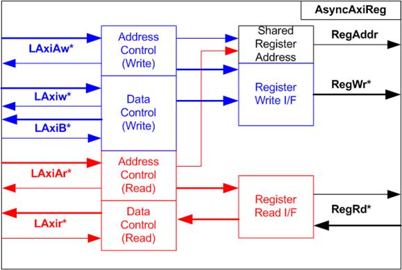
Figure 2‑12 AsyncAxiReg Interface
The signal on AXI4-Lite bus interface can be split into five groups, i.e., LAxiAw* (Write address channel), LAxiw* (Write data channel), LAxiB* (Write response channel), LAxiAr* (Read address channel), and LAxir* (Read data channel). More details to build custom logic for AXI4-Lite bus is described in following document.
According to AXI4-Lite standard, the write channel and the read channel are controlled independently. Also, the control and data interface of each channel are run separately. So, the logic inside AsyncAxiReg to interface with AXI4-Lite bus is split into four groups, i.e., Write control logic, Write data logic, Read control logic, and Read data logic as shown in the left side of Figure 2‑12. Write control I/F and Write data I/F of AXI4-Lite bus are latched and transferred to be Write register interface with clock-crossing registers. Similarly, Read control I/F of AXI4-Lite bus are latched and transferred to be Read register interface while Read data is returned from Register interface to AXI4-Lite through clock-crossing registers. In Register interface, RegAddr is shared signal for write and read access, so it loads the value from LAxiAw for write access or LAxiAr for read access.
The simple register interface is compatible to single-port RAM interface for write transaction. The read transaction of the register interface is slightly modified from RAM interface by adding RdReq and RdValid signals to controlling read latency time. The address of register interface is shared for write and read transaction, so user cannot write and read the register at the same time. The timing diagram of the register interface is shown in Figure 2‑13.
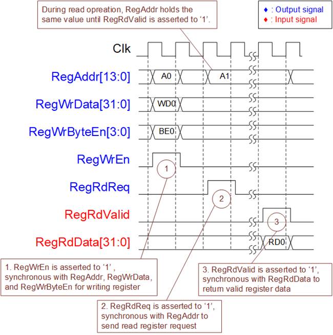
Figure 2‑13 Register interface timing diagram
1) To write register, the timing diagram is similar to single-port RAM interface. RegWrEn is asserted to �1� with the valid signal of RegAddr (Register address in 32-bit unit), RegWrData (write data of the register), and RegWrByteEn (the write byte enable). Byte enable has four bits to be the byte data valid. Bit[0], [1], [2] and [3] are equal to �1� when RegWrData[7:0], [15:8], [23:16] and [31:24] are valid respectively.
2) To read register, AsyncAxiReg asserts RegRdReq to �1� with the valid value of RegAddr. 32-bit data must be returned after receiving the read request. The slave must monitor RegRdReq signal to start the read transaction. During read operation, the address value (RegAddr) does not change the value until RegRdValid is asserted to �1�. So, the address can be used for selecting the returned data by using multiple-layer multiplexer.
3) The read data is returned on RegRdData bus by the slave with asserting RegRdValid to �1�. After that, AsyncAxiReg forwards the read value to LAxir* interface.
2.3.2 UserReg
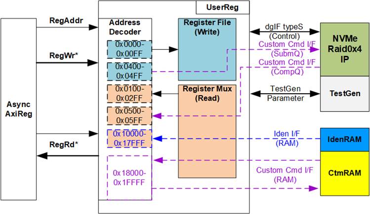
Figure 2‑14 UserReg Interface
The address range to map to UserReg is split into six areas, as shown in Figure 2‑14.
1) 0x0000 � 0x00FF: mapped to set the test parameters of NVMeRaid0x4 IP and TestGen. This area is write-access only.
2) 0x0400 � 0x04FF: mapped to set the test parameters of custom command interface (NVMeRaid0x4 IP). This area is write-access only.
3) 0x0100 � 0x02FF: mapped to read the status of NVMeRaid0x4 IP and TestGen. This area is read-access only.
4) 0x0500 � 0x05FF: mapped to read the status of custom command interface (NVMeRaid0x4 IP). This area is read-access only.
5) 0x10000 � 0x17FFF: mapped to read data from IdenRAM. This area is read-access only.
6) 0x18000 � 0x1FFFF: mapped to custom command RAM interface (NVMeRaid0x4 IP). Although this area supports both write-access and read-access, the demo shows only read-access by running SMART command.
Address decoder decodes the upper bit of RegAddr for selecting the active hardware. The register file inside UserReg is 32-bit bus size, so write byte enable (RegWrByteEn) is not used. To write hardware registers, the CPU must use 32-bit pointer to place 32-bit valid value on the write data bus.
To read register, three-step multiplexer is designed to select the read data within each address area. The lower bit of RegAddr is applied in each Register area to select the data. Next, the address decoder uses the upper bit to select the read data from each area for returning to CPU. Totally, the latency of read data is equal to three clock cycles, so RegRdValid is created by RegRdReq with asserting three D Flip-flops. More details of the address mapping within UserReg module are shown in Table 2‑2.
Table 2‑2 Register Map
|
Address |
Register Name |
Description |
|
Wr/Rd |
(Label in �nvmeipraid0x4test.c�) |
|
|
0x0000 � 0x00FF: Control signals of NVMeRaid0x4 IP and TestGen (Write access only) |
||
|
BA+0x0000 |
User Address (Low) Reg |
[31:0]: Input to be bit[31:0] of start address in 512-byte unit (UserAddr[31:0] of dgIF typeS for RAID0) |
|
(USRADRL_REG) |
||
|
BA+0x0004 |
User Address (High) Reg |
[15:0]: Input to be bit[47:32] of start address in 512-byte unit (UserAddr[47:32] of dgIF typeS for RAID0) |
|
(USRADRH_REG) |
||
|
BA+0x0008 |
User Length (Low) Reg |
[31:0]: Input to be bit[31:0] of transfer length in 512-byte unit (UserLen[31:0] of dgIF typeS for RAID0) |
|
(USRLENL_REG) |
||
|
BA+0x000C |
User Length (High) Reg |
[15:0]: Input to be bit[47:32] of transfer length in 512-byte unit (UserLen[47:32] of dgIF typeS for RAID0) |
|
(USRLENH_REG) |
||
|
BA+0x0010 |
User Command Reg |
[2:0]: Input to be user command (UserCmd of dgIF typeS for RAID0) (�000�: Identify, �001�: Shutdown, �010�: Write RAID, �011�: Read RAID, �100�: SMART, �110�: Flush, �101�/�111�: Reserved). When this register is written, new command request is sent to RAID0 for operating the new command. |
|
(USRCMD_REG) |
||
|
BA+0x0014 |
Test Pattern Reg |
[2:0]: Test pattern select �000�-Increment, �001�-Decrement, �010�-All 0, �011�-All 1, �100�-LFSR |
|
(PATTSEL_REG) |
||
|
BA+0x0020 |
NVMe Timeout Reg |
[31:0]: Input to be timeout value of NVMe-IP (TimeOutSet[31:0] of NVMe-IP) |
|
(NVMTIMEOUT_REG) |
||
|
0x0100 � 0x02FF: Status signals of NVMeRaid0x4 IP and TestGen (Read access only) |
||
|
BA+0x0100 |
User Status Reg |
[0]: UserBusy of dgIF typeS for RAID0 (�0�: Idle, �1�: Busy) [1]: UserError of dgIF typeS for RAID0 (�0�: Normal, �1�: Error) [2]: Data verification fail (�0�: Normal, �1�: Error) |
|
(USRSTS_REG) |
||
|
BA+0x0104 |
Total device size (Low) Reg |
[31:0]: Bit[31:0] of total capacity of RAID0 in 512-byte unit (LBASize[31:0] of dgIF typeS for RAID0) |
|
(LBASIZEL_REG) |
||
|
BA+0x0108 |
Total device size (High) Reg |
[15:0]: Bit[47:32] of total capacity of RAID0 in 512-byte unit (LBASize[47:32] of dgIF typeS for RAID0) |
|
(LBASIZEH_REG) |
||
|
(BA+0x0110)- (BA+0x011C) |
User Error Type CH#0-#3 Reg |
0x0110: NVMe-IP#0, 0x0114: NVMe-IP#1, 0x0118: NVMe-IP#2, 0x011C: NVMe-IP#3 [31:0]: Mapped to UserErrorType of NVMe-IP#0 - #3 successively. |
|
(USRERRTYPE0-3_REG) |
||
|
(BA+0x0120)- (BA+0x012C) |
PCIe Status CH#0-#3 Reg |
0x0120: NVMe-IP#0, 0x0124: NVMe-IP#1, 0x0128: NVMe-IP#2, 0x012C: NVMe-IP#3 [0]: PCIe linkup status from PCIe hard IP (�0�: No linkup, �1�: linkup) [3:2]: PCIe link speed from PCIe hard IP (�00�: Not linkup, �01�: PCIe Gen1, �10�: PCIe Gen2, �11�: PCIe Gen3) [7:4]: PCIe link width status from PCIe hard IP (�0001�: 1-lane, �0010�: 2-lane, �0100�: 4-lane, �1000�: 8-lane) [13:8]: Current LTSSM State of PCIe hard IP. Please see more details of LTSSM value in Integrated Block for PCIe datasheet. |
|
(PCIESTS0-3_REG) |
||
|
(BA+0x0130)- (BA+0x013C) |
Completion Status CH#0-#3 Reg |
0x0130: NVMe-IP#0, 0x0134: NVMe-IP#1, 0x0138: NVMe-IP#2, 0x013C: NVMe-IP#3 [15:0]: Status from Admin completion (AdmCompStatus[15:0] of NVMe-IP) [31:16]: Status from I/O completion (IOCompStatus[15:0] of NVMe-IP) |
|
(COMPSTS0-3_REG) |
||
|
(BA+0x0140)- (BA+0x014C) |
NVMe CAP CH#0-#3 Reg |
0x0140: NVMe-IP#0, 0x0144: NVMe-IP#1, 0x0148: NVMe-IP#2, 0x014C: NVMe-IP#3 [31:0]: Mapped to NVMeCAPReg[31:0] of NVMe-IP#0 - #3 successively. |
|
(NVMCAP0-3_REG) |
||
|
(BA+0x0150)- (BA+0x015C) |
NVMe IP Test pin CH#0-#3 Reg |
0x0150: NVMe-IP#0, 0x0154: NVMe-IP#1, 0x0158: NVMe-IP#2, 0x015C: NVMe-IP#3 [31:0]: TestPin[31:0] output from NVMe-IP#0 - #3 successively. |
|
(NVMTESTPIN0-3_REG) |
||
|
Address |
Register Name |
Description |
|
Wr/Rd |
(Label in �nvmeipraid0x4test.c�) |
|
|
0x0100 � 0x02FF: Status signals of NVMeRaid0x4 IP and TestGen (Read access only) |
||
|
BA+0x0200 |
Data Failure Address(Low) Reg |
[31:0]: Bit[31:0] of the byte address at the 1st failure data in Read command |
|
(RDFAILNOL_REG) |
||
|
BA+0x0204 |
Data Failure Address(High) Reg |
[24:0]: Bit[56:32] of the byte address at the 1st failure data in Read command |
|
(RDFAILNOH_REG) |
||
|
BA+0x0208 |
Current test byte (Low) Reg |
[31:0]: Bit[31:0] of the current test data size in TestGen module |
|
(CURTESTSIZEL_REG) |
||
|
BA+0x020C |
Current test byte (High) Reg |
[24:0]: Bit[56:32] of the current test data size of TestGen module |
|
(CURTESTSIZEH_REG) |
||
|
(BA+0x0280)- (BA+0x02BC) |
Expected value Word0-15 Reg |
0x280: Bit[31:0], 0x284: Bit[63:32], �, 0x2BC: Bit[511:480] The expected data at the 1st failure data in Read command successively. |
|
(EXPPATW0-W15_REG) |
||
|
(BA+0x02C0)- (BA+0x02FC) |
Read value Word0-15 Reg |
0x2C0: Bit[31:0], 0x2C4: Bit[63:32], �, 0x2FC: Bit[511:480] The read data at the 1st failure data in Read command successively. |
|
(RDPATW0-W15_REG) |
||
|
0x0400 � 0x0FFF: Custom command of NVMeRaid0x4 IP |
||
|
(BA+0x0400)- (BA+0x04FF) |
Custom Submission Queue CH#0�#3 Reg |
[31:0]: Submission queue entry of SMART and Flush command. Input to be CtmSubmDW0-DW15 of NVMe-IP#0-#3 successively. 0x400: DW0, 0x404: DW1, �, 0x43C: DW15 of NVMe-IP#0 0x440: DW0, 0x444: DW1, �, 0x47C: DW15 of NVMe-IP#1 0x480: DW0, 0x484: DW1, �, 0x4BC: DW15 of NVMe-IP#2 0x4C0: DW0, 0x4C4: DW1, �, 0x4FC: DW15 of NVMe-IP#3 |
|
Wr |
(CTMSUBMQ0-3_REG) |
|
|
(BA+0x0500)- (BA+0x053F) |
Custom Completion Queue CH#0�#3 Reg |
[31:0]: CtmCompDW0-DW3 output from NVMe-IP#0-#3 successively. 0x500: DW0, 0x504: DW1, �, 0x50C: DW3 of NVMe-IP#0 0x510: DW0, 0x514: DW1, �, 0x51C: DW3 of NVMe-IP#1 0x520: DW0, 0x514: DW1, �, 0x52C: DW3 of NVMe-IP#2 0x530: DW0, 0x514: DW1, �, 0x53C: DW3 of NVMe-IP#3 |
|
Rd |
(CTMCOMPQ0-3_REG) |
|
|
BA+0x0800 |
IP Version Reg |
[31:0]: IP version number (IPVersion[31:0] of NVMe-IP) |
|
Rd |
(IPVERSION_REG) |
|
|
0x10000 � 0x1FFFF: Identify RAM and Custom RAM |
||
|
(BA+0x10000) � (BA+0x17FFF) |
Identify Controller Data CH#0-#3 |
0x10000-0x11FFF: NVMe-IP#0, 0x12000-0x13FFF: NVMe-IP#1, 0x14000-0x15FFF: NVMe-IP#2, 0x16000-0x17FFF: NVMe-IP#3 Lower 4Kbyte stores Identify controller data of NVMe-IP#0-#3 Upper 4Kbyte stores Identify namespace data of NVMe-IP#0-#3 |
|
Rd |
(IDENCTRL0-3_REG/ IDENNAME0-3_REG) |
|
|
(BA+0x18000) � (BA+0x1FFFF) |
Custom command Ram CH#0-#3
|
0x18000-0x19FFF: NVMe-IP#0, 0x1A000-0x1BFFF: NVMe-IP#1, 0x1C000-0x1DFFF: NVMe-IP#2, 0x1E000-0x1FFFF: NVMe-IP#3 8K byte CtmRAM interface of NVMe-IP#0-#3. Used to store 512-byte data output from SMART Command. |
|
Wr/Rd |
(CTMRAM0-3_REG) |
|
3 CPU Firmware
3.1 Test firmware (nvmeipraid0x4test.c)
After system boot-up, CPU runs following steps to finish the initialization process.
1) CPU initializes its peripherals such as UART and Timer.
2) CPU waits until PCIe connection of all channels are linked up (PCISTS0-3_REG[0]=�1�).
3) CPU waits until NVMeRaid0x4-IP completes initialization process (USRSTS_REG[0]=�0�). The error message is displayed and the process stops when some errors are found.
4) CPU displays the number of PCIe lanes and PCIe speed of all channels by reading PCISTS0-3_REG[7:2].
5) CPU checks LBA Size of NVMe SSDs. When LBA Size is 4k byte, the process stops and the error message is displayed.
6) CPU displays the main menu. There are six menus for running six commands with RAID0, i.e., Identify, Write, Read, SMART, Flush, and Shutdown.
More details of each command are described as follows.
3.1.1 Identify command
The step to operate Identify command is described as follows.
1) Set USRCMD_REG=�000� to send Identify command to all NVMe SSDs. Command request is sent to NVMeRaid0x4-IP. After that, busy flag (USRSTS_REG[0]) changes from �0� to �1�.
2) CPU waits until the operation is completed or some errors are found by monitoring USRSTS_REG[1:0].
Bit[0] is de-asserted to �0� when command is completed. After that, the data from Identify command is stored to IdenRAM.
Bit[1] is asserted to �1� when some errors are detected. The error message is displayed on the console to show the error details (read from USRERRTYPE0-3_REG[31:0]). Finally, the process is stopped.
3) After busy flag (USRSTS_REG[0]) is de-asserted to �0�, CPU decodes SSD model name from IdenRAM (IDENCTRL0-3_REG) and reads RAID capacity (LBASIZE_REG) from NVMeRaid0x4-IP output to display on the console.
3.1.2 Write/Read command
The step to operate Write/Read command is described as follows.
1) Receive input parameters from user through Serial console, i.e., start address, transfer length, and test pattern. When some inputs are invalid, the operation is cancelled.
2) Set the input parameters to hardware registers, i.e., USRADRL/H_REG, USRLENL/H_REG, and PATTSEL_REG.
3) Set USRCMD_REG[2:0]=�010� for Write command or �011� for Read command. After that, the new command request is sent to NVMeRaid0x4-IP for running Write or Read command. Busy flag (USRSTS_REG[0]) changes from �0� to �1�.
4) CPU waits until the operation is completed or some errors (except verification error) are found by monitoring USRSTS_REG[2:0].
Bit[0] is de-asserted to �0� when command is completed.
Bit[1] is asserted to �1� when some errors are detected. The error message is displayed on the console to show the error details and the process is stopped.
Bit[2] is asserted to �1� when data verification is failed. The verification error message is displayed on the console to show the error details. In this condition, CPU is still running until the operation is done or user presses any key(s) to cancel operation.
When the operation does not finish, current transfer size read from CURTESTSIZE_REG is displayed every second.
5) After busy flag (USRSTS_REG[0]) is de-asserted to �0�, CPU calculates and displays the test result on the console, i.e., total time usage, total transfer size, and transfer speed.
3.1.3 SMART Command,
The step to operate SMART command is described as follows.
1) Set 16 Dwords of Submission queue entry (CTMSUBMQ0-3_REG) to be SMART command value.
2) Set USRCMD_REG[2:0]=�100� to send SMART command to all NVMe SSDs. Command request is sent to NVMeRaid0x4-IP. After that, busy flag (USRSTS_REG[0]) changes from �0� to �1�.
3) CPU waits until the operation is completed or some errors are found by monitoring USRSTS_REG[1:0].
Bit[0] is de-asserted to �0� when command is completed. After that, the data from SMART command is stored to CtmRAM.
Bit[1] is asserted to �1� when some errors are detected. The error message is displayed on the console to show the error details (read from USRERRTYPE0-3_REG[31:0]). Finally, the process is stopped.
4) After busy flag (USRSTS_REG[0]) is de-asserted to �0�, CPU decodes SMART command information from CtmRAM (CTMRAM0-3_REG), i.e., Temperature, Total Data Read, Total Data Written, Power On Cycles, Power On Hours, and Number of Unsafe Shutdown.
More details of SMART log are described in NVM Express Specification.
https://nvmexpress.org/resources/specifications/
3.1.4 Flush Command
The step to operate Flush command is described as follows.
1) Set 16 Dwords of Submission queue entry (CTMSUBMQ0-3_REG) to be Flush command value.
2) Set USRCMD_REG[2:0]=�110� to send Flush command to all NVMe SSDs. Command request is sent to NVMeRaid0x4-IP. After that, busy flag (USRSTS_REG[0]) changes from �0� to �1�.
3) CPU waits until the operation is completed or some errors are found by monitoring USRSTS_REG[1:0].
Bit[0] is de-asserted to �0� when command is completed. After that, CPU goes back to the main menu.
Bit[1] is asserted to �1� when some errors are detected. The error message is displayed on the console to show the error details (read from USRERRTYPE0-3_REG[31:0]). Finally, the process is stopped.
3.1.5 Shutdown Command
The step to operate Shutdown command is described as follows.
1) Set USRCMD_REG[2:0]=�001� to send Shutdown command to all NVMe SSDs. Command request is sent to NVMeRaid0x4-IP. After that, busy flag (USRSTS_REG[0]) changes from �0� to �1�.
2) CPU waits until the operation is completed or some errors are found by monitoring USRSTS_REG[1:0].
Bit[0] is de-asserted to �0� when command is completed.
Bit[1] is asserted to �1� when some errors are detected. The error message is displayed on the console to show the error details (read from USRERRTYPE0-3_REG[31:0]). Finally, the process is stopped.
3) After busy flag (USRSTS_REG[0]) is de-asserted to �0�, the four SSDs change to inactive status. All NVMe-IPs change to inactive state and the CPU cannot receive new command from user. The user must power off the test system.
3.2 Function list in Test firmware
|
int exec_ctm(unsigned int user_cmd) |
|
|
Parameters |
user_cmd: 4-SMART command, 6-Flush command |
|
Return value |
0: No error, -1: Some errors are found in the NVMe-IP |
|
Description |
Run SMART command or Flush command, following in topic 3.1.3 (SMART Command,) and 3.1.4 (Flush Command). |
|
int flush_ctmnvm(void) |
|
|
Parameters |
None |
|
Return value |
0: No error, -1: Some errors are found in the NVMe-IP |
|
Description |
Set Flush command to CTMSUBMQ0-3_REG and call exec_ctm function to start Flush command. |
|
unsigned long long get_cursize(void) |
|
|
Parameters |
None |
|
Return value |
Read value of CURTESTSIZEH/L_REG |
|
Description |
Read CURTESTSIZEH/L_REG and return read value as function result. |
|
int get_param(userin_struct* userin) |
|
|
Parameters |
userin: Three inputs from user, i.e., start address, total length in 512-byte unit, and test pattern |
|
Return value |
0: Valid input, -1: Invalid input |
|
Description |
Receive the input parameters from the user and verify the value. When the input is invalid, the function returns -1. Otherwise, all inputs are updated to userin parameter. |
|
void iden_dev(void) |
|
|
Parameters |
None |
|
Return value |
None |
|
Description |
Run Identify command, following in topic 3.1.1 (Identify command). |
|
void shutdown_dev(void) |
|
|
Parameters |
None |
|
Return value |
None |
|
Description |
Run Shutdown command, following in topic 3.1.5 (Shutdown Command) |
|
void show_error(void) |
|
|
Parameters |
None |
|
Return value |
None |
|
Description |
Read USRERRTYPE0-3_REG, decode the error flag, and display error message following the error flag of each channel. |
|
void show_pciestat(void) |
|
|
Parameters |
None |
|
Return value |
None |
|
Description |
Read PCIESTS0-3_REG until the read value from two read times is stable. After that, display the read value on the console. |
|
void show_result(void) |
|
|
Parameters |
None |
|
Return value |
None |
|
Description |
Read CURTESTSIZEL/H _REG to display total transfer size. Read the global parameters (timer_val and timer_upper_val) and calculate total time usage to display in usec, msec, or sec unit. Finally, transfer performance is calculated and displayed on MB/s unit. |
|
void show_size(unsigned long long size_input) |
|
|
Parameters |
size_input: transfer size to display on the console |
|
Return value |
None |
|
Description |
Calculate and display the input value in MByte, GByte, or TByte unit |
|
void show_smart_hex(unsigned char *char_ptr16B) |
|
|
Parameters |
*char_ptr16B |
|
Return value |
None |
|
Description |
Display SMART data as hexadecimal unit. |
|
void show_smart_raw(unsigned char *char_ptr16B) |
|
|
Parameters |
*char_ptr16B |
|
Return value |
None |
|
Description |
Display SMART data as decimal unit when the input value is less than 4 MB. Otherwise, display overflow message. |
|
void show_smart_unit(unsigned char *char_ptr16B) |
|
|
Parameters |
*char_ptr16B |
|
Return value |
None |
|
Description |
Display SMART data as GB or TB unit. When the input value is more than limit (500 PB), overflow message is displayed instead. |
|
void show_vererr(void) |
|
|
Parameters |
None |
|
Return value |
None |
|
Description |
Read RDFAILNOL/H_REG (error byte address), EXPPATW0-W15_REG (expected value), and RDPATW0-W15_REG (read value) to display verification error details on the console. |
|
int smart_ctmadm(void) |
|
|
Parameters |
None |
|
Return value |
0: No error, -1: Some errors are found in the NVMe-IP |
|
Description |
Set SMART command to CTMSUBMQ0-3_REG and call exec_ctm function to start SMART command. Finally, decode and display SMART information on the console |
|
int wrrd_dev(unsigned int user_cmd) |
|
|
Parameters |
user_cmd: 2-Write command, 3-Read command |
|
Return value |
0: No error, -1: Receive invalid input or some errors are found. |
|
Description |
Run Write command or Read command, following in topic 3.1.2 (Write/Read command) |
4 Example Test Result
The example test result when running RAID0 demo system by using two 512 GB Samsung 960 Pro SSDs and two 512 GB Samsung 970 Pro SSDs is shown in Figure 4‑1.
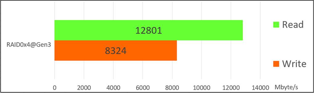
Figure 4‑1 Performance of 4-ch RAID0 demo by using Samsung Pro 960/970 SSD
When running 4-ch RAID0 with 4 SSDs@Gen3 speed, write performance is about 8300 Mbyte/sec and read performance is about 12800 Mbyte/sec.
5 Revision History
|
Revision |
Date |
Description |
|
1.0 |
12-Nov-19 |
Initial version release |
|
1.1 |
1-Mar-21 |
Update memory map |
Copyright: 2019 Design Gateway Co,Ltd.