NVMeSW IP Core reference design manual
Rev1.1 17-Aug-23
1 NVMe
NVM Express (NVMe) defines the interface for the host controller to access solid state drive (SSD) by PCI Express. NVM Express optimizes the process to issue command and completion by using only two registers (Command issue and Command completion). Also, NVMe supports parallel operation by supporting up to 64K commands within single queue. 64K command entries improves transfer performance for both sequential and random access.
In PCIe SSD market, two standards are used, i.e. AHCI and NVMe. AHCI is the old standard to provide the interface for SATA hard disk drive while NVMe is optimized for non-volatile memory, like SSD. The comparison between both AHCI and NVMe protocol in more details is described in “A Comparison of NVMe and AHCI” document.
https://sata-io.org/system/files/member-downloads/NVMe%20and%20AHCI_%20_long_.pdf
The example of NVMe storage device is shown in http://www.nvmexpress.org/products/.
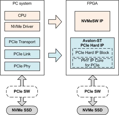
Figure 1‑1 NVMe protocol layer
To access NVMe SSD, the general system implements NVMe driver running on the processor, as shown in the left side of Figure 1‑1. The physical connection of NVMe standard is PCIe connector which is one-to-one type, so one PCIe host can connect to one PCIe device. When many SSDs must be connected to the one host, PCIe switch must be applied to extend the number of SSDs. When PCIe switch is applied, the driver on the processor must support to scan the NVMe SSD operating under PCIe switch.
NVMeSW-IP implements NVMe driver to access NVMe SSD and the function to scan NVMe SSD through one PCIe switch by using pure-hardware logic. So, user can access NVMe SSD without including any processor and driver by using NVMeSW-IP in FPGA board.
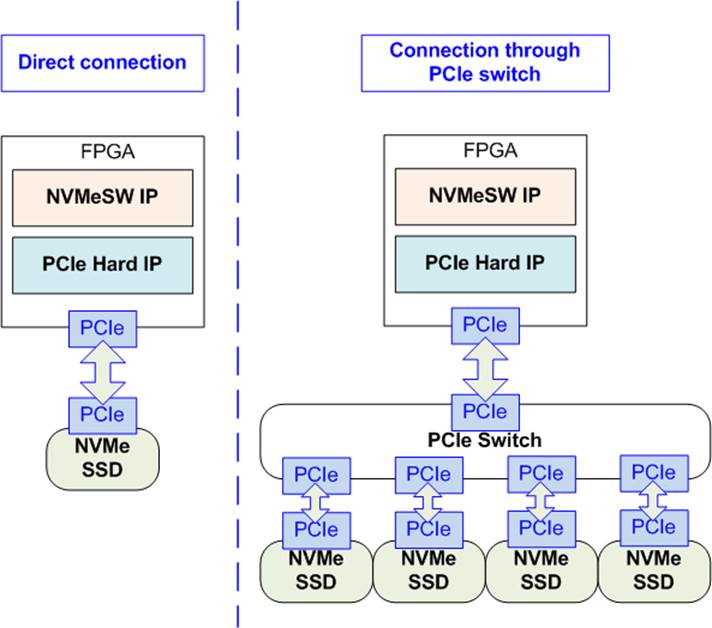
Figure 1‑2 Direct connection and PCIe switch connection
Figure 1‑2 shows two hardware connections for connecting NVMeSW-IP to NVMe SSD. The left side is the direct connection when one PCIe SSD is applied. PCIe connector of FPGA connects to an NVMe SSD without the intermediate hardware.
The right side shows the connection through PCIe switch when multiple SSDs must be controlled by one NVMeSW-IP. Though the number of connected SSDs is increased, transfer speed is same. NVMeSW-IP can operate with one SSD at a time. Also, the latency to transfer packet between NVMeSW-IP and the NVMe SSD is increased when connecting the SSD through PCIe switch. Write performance of some SSDs may be little dropped because of more latency time.
According to PCIe specification, one PCIe switch supports up to 32 NVMe SSDs, but NVMeSW-IP is designed to support up to 4 NVMe SSDs. Supporting more devices is as optional.
2 Hardware overview
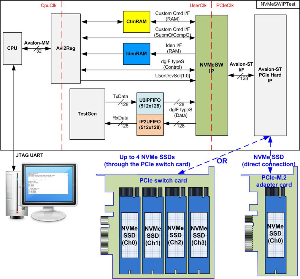
Figure 2‑1 NVMeSW-IP demo hardware
The hardware system can be split into three groups, i.e. TestGen, NVMe, and CPU. TestGen is the test logic to generate test data stream for NVMeSW-IP through U2IPFIFO. Also, TestGen reads data stream output from NVMeSW-IP through IP2UFIFO, and then verify it. NVMe includes the NVMeSW-IP and the PCIe hard IP (Avalon-ST PCIe hard IP). NVMe supports to access NVMe SSD directly or through PCIe switch. CPU and Avl2Reg are designed to interface with user through JTAG UART. User can set command and the test parameters through JTAG UART. Also, the current status of the test hardware is monitored by user through JTAG UART. The CPU firmware must be implemented to control the sequence for operating each command.
There are three clock domains displayed in Figure 2‑1, i.e. CpuClk, UserClk, and PCIeClk. CpuClk is the clock domain of CPU and its peripherals. This clock must be stable clock which is independent from the other hardware interface. PCIeClk is the clock output from PCIe hard IP to synchronous with data stream of 128-bit Avalon-ST interface. When the PCIe hard IP is set to 4 lane PCIe Gen3, PCIeClk frequency is equal to 250 MHz. UserClk is the example user clock domain which is independent from the other clock domains. So, UserClk is the main clock domain for running the user interface of NVMeSW-IP, RAM, FIFO, and TestGen. According to NVMeSW-IP datasheet, clock frequency of UserClk must be more than or equal to PCIeClk. In this reference design, UserClk is equal to 275 MHz.
To test data interface of NVMeSW-IP, four memory blocks are implemented, i.e. CtmRAM, IdenRAM, U2IPFIFO, and IP2UFIFO. CtmRAM stores returned data from SMART command while IdenRAM stores returned data from Identify command. U2IPFIFO stores data for Write command while IP2UFIFO stores data for Read command. TestGen is designed to monitor flow control signal of U2IPFIFO and IP2UFIFO to be always read and write data when the FIFO is ready. So, the FIFO depth is not large by setting to 512 x 128 bit and implemented by Block memory. When running SMART command or Identify command, the returned data from the command is processed on CPU. So, another side of CtmRAM and IdenRAM is connected to Avl2Reg to allow CPU accessing through Avalon-MM bus.
More details of the hardware are described as follows.
2.1 TestGen
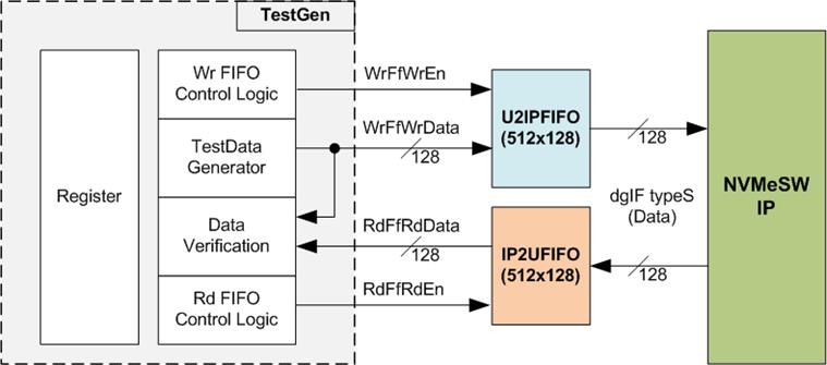
Figure 2‑2 TestGen interface
TestGen module is the test logic to send test data to NVMeSW-IP through U2IPFIFO when operating Write command. Also, the test data is fed to be the expected value to verify the read data from NVMeSW-IP through IP2UFIFO when operating Read command. Control logic asserts Write enable and Read enable to ‘1’ when the FIFOs are ready. Data bandwidth of TestGen is matched to NVMeSW-IP by running at the same clock and using same data bus size, so NVMeSW-IP can transfer data with U2IPFIFO and IP2UFIFO without waiting data ready. As a result, the test logic shows the best performance to write and read data with the SSD through NVMeSW-IP.
Register file in the TestGen receives test parameters from user, i.e. total transfer size, transfer direction, verification enable, and test pattern selector. So, the internal logic includes the counter to control total transfer size of test data. The details of hardware logic of TestGen are shown in Figure 2‑3.
Figure 2‑3 TestGen hardware
As shown in the right side of Figure 2‑3, flow control signals of FIFO are WrFfAFull and RdFfEmpty. When FIFO is almost full during write operation (WrFfAFull=’1’), WrFfWrEn is de-asserted to ‘0’ to pause data sending to FIFO. For read operation, when FIFO has data (RdFfEmpty=‘0’), the logic reads data from FIFO to compare with the expected data by asserting RdFfRdEn to ‘1’.
The logic in the left side of Figure 2‑3 is designed to count transfer size. When total data count is equal to the end size (set by user), write enable or read enable of FIFO is de-asserted to ‘0’. So, the total data count to write FIFO or read FIFO is controlled by user.
The lower side of Figure 2‑3 shows the details to generate test data for writing to FIFO or verifying data from FIFO. There are five patterns to generate, i.e. all zero, all one, 32-bit incremental data, 32-bit decremental data, and LFSR counter. All zero and all one are fixed value to select test data through Pattern Selector. While 32-bit incremental data is designed by using 53-bit counter. The decremental data can be designed by connecting NOT logic to increment data. The LFSR pattern is designed by using LFSR counter. The equation of LFSR is x^31 + x^21 + x + 1. Data bus size of TestGen is 128-bit, so four 32-bit LFSR data must be generated within one clock. The logic to design LFSR must use look-ahead style to generate four LFSR data in the same clock.
When creating all zero or all one pattern, every bit of data is fixed zero or one respectively. While other patterns are designed by separating the data as two parts to create unique test data in every 512-byte data. As shown in Figure 2‑4, 512-byte data consists of 64 bit header in Dword#0 and Dword#1 and the test data in remaining words of 512-byte data (Dword#2 – Dword#127).
Figure 2‑4 Test pattern format in each 512-byte data for Increment/Decrement/LFSR pattern
64-bit header is created by using the address in 512-byte unit. Therefore, Address counter inside TestData Generator generates the current address to be 64-bit header data. The initial value of the address counter is set by user. After that, the address counter is incremented when finishing to transfer 512-byte data.
Test data is fed to be write data to the FIFO or the expected data comparing with the read data from FIFO. Fail flag is asserted to ‘1’ when data verification is failed. The example of timing diagram to write data to FIFO is shown as follows.
Figure 2‑5 Timing diagram of Write operation in TestGen
1) WrPattStart is asserted to ‘1’ for one clock cycle when user sets the register to start write operation. In the next clock, rWrTrans is asserted to ‘1’ to enable the control logic for generating write enable to FIFO.
2) Write enable to FIFO (rWrFfWrEn) is asserted to ‘1’ when two conditions are met. First, rWrTrans must be asserted to ‘1’ during the write operation being active. Second, the FIFO must not be full by monitoring WrFfAFull=’0’.
3) The write enable is fed back to be counter enable to count total data in the write operation.
4) If FIFO is almost full (WrFfAFull=’1’), the write process is paused by de-asserting rWrFfWrEn to ‘0’.
5) When total data count is equal to the set value, rWrTrans is de-asserted to ‘0’. At the same time, rWrFfWrEn is also de-asserted to ‘0’ to stop data generating.
For read timing diagram, read enable of FIFO is controlled by empty flag of FIFO. Comparing to write enable, the read enable signal is not stopped by total count and not started by start flag. When the read enable is asserted to ‘1’, the data counter and address counter are also increment for counting total data and generating the header of expect value.
2.2 NVMe
Figure 2‑6 NVMe hardware
Figure 2‑6 shows the example to interface NVMeSW-IP in the reference design. The user interface of NVMeSW-IP is split into control interface and data interface. The control interface receives the parameters of the command through custom command interface or dgIF typeS, depending on the command. Custom command interface is used when operating SMART command or Flush command.
The data interface of NVMeSW-IP has four signal groups, i.e. custom command RAM interface, Identify interface, FIFO input interface (dgIF types), and FIFO output interface (dgIF types). Data bus width of all signal groups is 128-bit. The custom command RAM interface is bi-directional interface while the other interfaces are one directional interface. In the reference design, the custom command RAM interface is used to transfer data of SMART command from NVMeSW-IP to Avl2Reg only.
2.2.1 NVMeSW-IP
The NVMeSW-IP implements NVMe protocol of the host side to access one NVMe SSD directly or multiple SSDs through PCIe switch. The NVMeSW-IP supports six commands, i.e. Write, Read, Identify, Shutdown, SMART, and Flush. NVMeSW-IP can connect to the PCIe hard IP directly. More details of NVMeSW-IP are described in datasheet.
https://dgway.com/products/IP/NVMe-IP/dg_nvmeswip_datasheet_intel_en.pdf
2.2.2 Avalon-ST PCIe Hard IP
This block is hard IP in IntelFPGA device which implements Physical, Data Link and Transaction Layers of PCIe specification. More details are described in IntelFPGA document.
Intel Arria10 and Intel Cyclone 10 GX Avalon-ST Interface for PCIe Solutions User Guide
https://www.intel.com/content/dam/www/programmable/us/en/pdfs/literature/ug/ug_a10_pcie_avst.pdf
2.2.3 Two-Port RAM
Two of 2-Port RAMs are implemented in the reference design to store data from Identify command and SMART command.
IdenRAM is simple dual-port RAM which has one read port and one write port. The data size of Identify command is 8Kbyte, so IdenRAM size is 8Kbyte. NVMeSW-IP and Avl2Reg have different data bus size, so IdenRAM sets the different bus size for write port and read port. The data interface of NVMeSW-IP (write port) is 128-bit while the interface of Avl2Reg (read port) is 32-bit. Furthermore, NVMeSW-IP has double word enable to write only 32-bit data in some cases. The RAM setting on IP catalog of QuartusII supports the write byte enable. So, one bit of double word enable is extended to be 4-bit write byte enable as shown in Figure 2‑7.
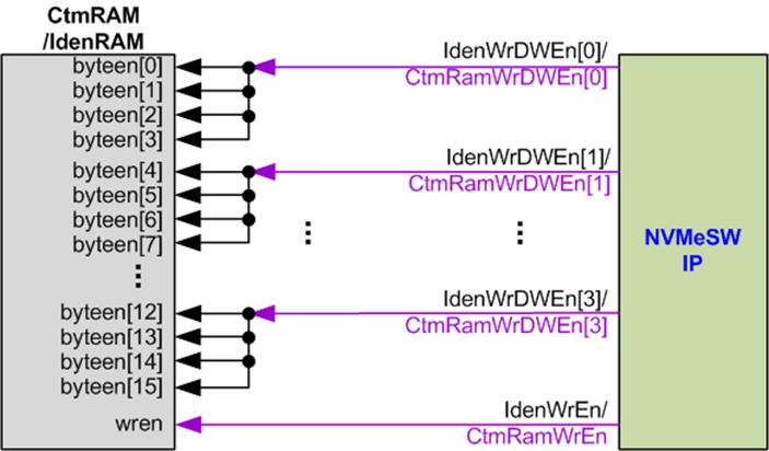
Figure 2‑7 Word enable to be byte write enable connection
Bit[0] of WrDWEn is fed to bit[3:0] of IdenRAM byte write enable. Bit[1] of WrDWEn is applied to generate bit[7:4] of IdenRAM write byte enable, and so on.
Similar to IdenRAM, CtmRAM supports byte write enable and double word enable of custom interface is connected to 4-bit write byte enable. Unlike IdenRAM, CtmRAM is true dual-port RAM (two read ports and two write ports) to allow NVMeSW-IP and Avl2Reg writing and reading data. The data width of both interfaces generated by IP catalog is 128-bit. The small logic is designed to convert data bus from 128-bit to be 32-bit for Avl2Reg access in write and read transaction. Two lower address bits are applied to select the active double word from 128-bit data. CtmRAM is implemented by 8Kbyte RAM for the future support though the data size of SMART command is 512-byte.
2.3 CPU and Peripherals
32-bit Avalon-MM bus is applied to be the bus interface for CPU accessing the peripherals such as Timer and JTAG UART. To control and monitor the test logic of NVMeSW-IP, the test logic is connected to CPU as a peripheral on 32-bit Avalon-MM bus. CPU assigns the different base address and the address range for each peripheral.
In the reference design, the CPU system is built with one additional peripheral to access the test logic. The base address and the range for accessing the test logic are defined in the CPU system. So, the hardware logic must be designed to support Avalon-MM bus standard for writing and reading the register. Avl2Reg module is designed to connect the CPU system as shown in Figure 2‑8.
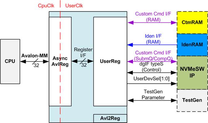
Figure 2‑8 CPU and peripherals hardware
Avl2Reg consists of AsyncAvlReg and UserReg. AsyncAvlReg is designed to convert the Avalon-MM signals to be the simple register interface which has 32-bit data bus size (similar to Avalon-MM data bus size). In addition, AsyncAvlReg includes asynchronous logic to support clock crossing between CpuClk domain and UserClk domain.
UserReg includes the register file of the parameters and the status signals to control the other modules, i.e. CtmRAM, IdenRAM, NVMeSW-IP, and TestGen. More details of AsyncAvlReg and UserReg are described as follows.
2.3.1 AsyncAvlReg
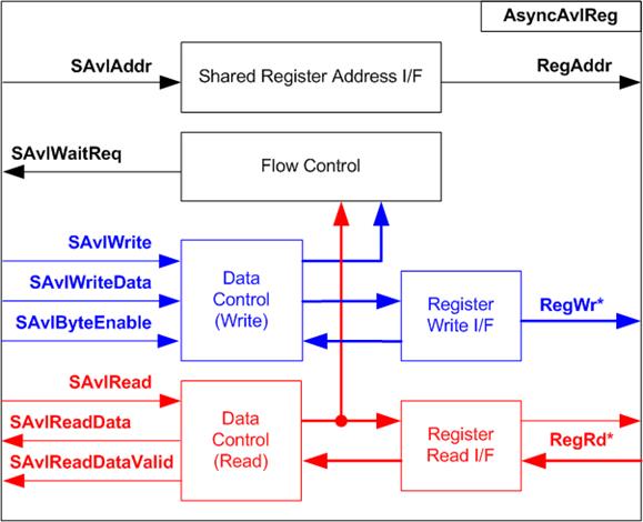
Figure 2‑9 AsyncAvlReg Interface
The signal on Avalon-MM bus interface can be split into three groups, i.e. Write channel (blue color), Read channel (red color) and Shared control channel (black color). More details of Avalon-MM interface specification is described in following document.
https://www.intel.com/content/dam/www/programmable/us/en/pdfs/literature/manual/mnl_avalon_spec.pdf
According to Avalon-MM specification, one command (write or read) can be operated at a time. The logic inside AsyncAvlReg is split into three groups, i.e. Write control logic, Read control logic and Flow control logic. Flow control logic to control SAvlWaitReq is designed to hold the next request from Avalon-MM interface while the current request is operating. Write control I/F and Write data I/F of Avalon-MM bus are latched and transferred as Write register. While Read control I/F and Read data I/F of Avalon-MM bus are latched and transferred as Read register. Address I/F of Avalon-MM is latched and transferred to Address register interface as well.
The simple register interface is designed to compatible to general RAM interface for write transaction. The read transaction of the register interface is little modified from RAM interface by adding RdReq signal. The address of register interface is shared for write and read transaction. So, user cannot write and read the register at the same time. The timing diagram of the register interface is shown in Figure 2‑10
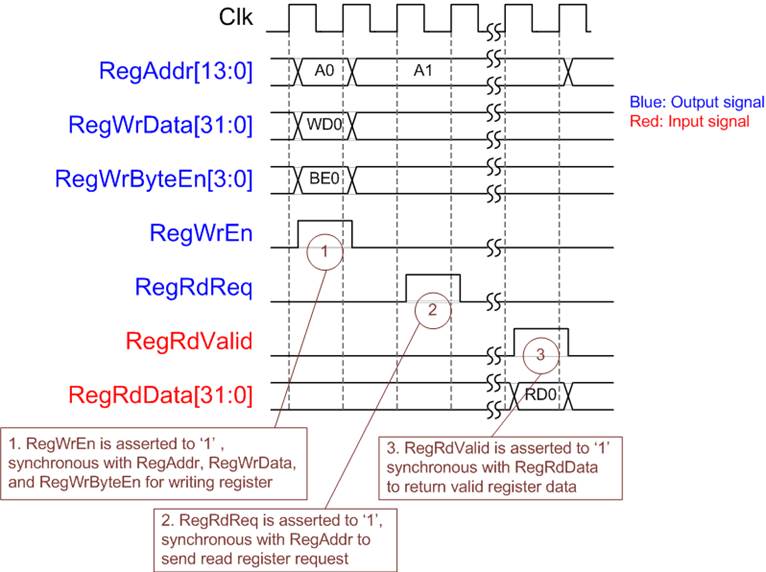
Figure 2‑10 Register interface timing diagram
1) To write register, the timing diagram is same as general RAM interface. RegWrEn is asserted to ‘1’ with the valid signal of RegAddr (Register address in 32-bit unit), RegWrData (write data of the register), and RegWrByteEn (the write byte enable). Byte enable has four bit to be the byte data valid, i.e. bit[0] for RegWrData[7:0], bit[1] for RegWrData[15:8], and so on.
2) To read register, AsyncAvlReg asserts RegRdReq to ’1’ with the valid value of RegAddr. 32-bit data must be returned after receiving the read request. The slave must monitor RegRdReq signal to start the read transaction.
3) The read data is returned on RegRdData bus by the slave with asserting RegRdValid to ‘1’. After that, AsyncAvlReg forwards the read value to SAvlRead interface.
2.3.2 UserReg
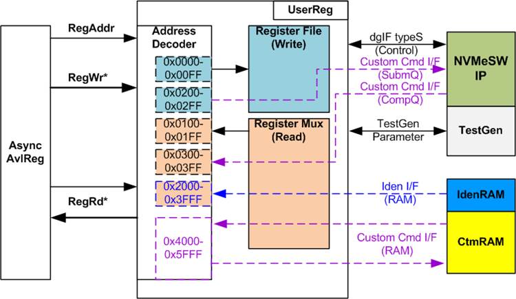
Figure 2‑11 UserReg Interface
The address range to map to UserReg is split into six areas, as shown in Figure 2‑11.
1) 0x0000 – 0x00FF: mapped to set the test parameters of NVMeSW-IP and TestGen. This area is write access only.
2) 0x0200 – 0x02FF: mapped to set the test parameters of custom command interface (NVMeSW-IP). This area is write access only.
3) 0x0100 – 0x01FF: mapped to read the status of NVMeSW-IP and TestGen. This area is read access only.
4) 0x0300 – 0x03FF: mapped to read the status of custom command interface (NVMeSW-IP). This area is read access only.
5) 0x2000 – 0x3FFF: mapped to read data from IdenRAM. This area is read access only.
6) 0x4000 – 0x5FFF: mapped to custom command RAM interface (NVMeSW-IP). This area supports write access and read access. The demo shows only read access by running SMART command.
Address decoder decodes the upper bit of RegAddr for selecting the active hardware. The register file inside UserReg is 32-bit bus size, so write byte enable (RegWrByteEn) is not used. To set the parameters in the hardware, the CPU must use 32-bit pointer to force 32-bit valid value of the write data.
To read register, two step multiplexers are designed. Register Mux is the data multiplexer to select the read data within each address area. The lower bit of RegAddr is applied in the Register Mux. Next, the address decoder uses the upper bit to select the read data from each area for returning to CPU. Totally, the latency of read data is equal to two clock cycles, so RegRdValid is created by RegRdReq with asserting two D Flip-flips.
More details of the address mapping within UserReg module is shown in Table 2‑1.
Table 2‑1 Register Map
|
Address |
Register Name |
Description |
|
Wr/Rd |
(Label in the “nvmeswiptest.c”) |
|
|
0x0000 – 0x00FF: Control signals of NVMeSW-IP and TestGen (Write access only) |
||
|
BA+0x0000 |
User Address (Low) Reg |
[31:0]: Input to be start address as 512-byte unit (UserAddr[31:0] of dgIF typeS) |
|
(USRADRL_REG) |
||
|
BA+0x0004 |
User Address (High) Reg |
[15:0]: Input to be start address as 512-byte unit (UserAddr[47:32] of dgIF typeS) |
|
(USRADRH_REG) |
||
|
BA+0x0008 |
User Length (Low) Reg |
[31:0]: Input to be transfer length as 512-byte unit (UserLen[31:0] of dgIF typeS) |
|
(USRLENL_REG) |
||
|
BA+0x000C |
User Length (High) Reg |
[15:0]: Input to be transfer length as 512-byte unit (UserLen[47:32] of dgIF typeS) |
|
(USRLENH_REG) |
||
|
BA+0x0010 |
User Command Reg |
[2:0]: Input to be user command (UserCmd of dgIF typeS for NVMeSW-IP) “000”: Identify, “001”: Shutdown, “010”: Write SSD, “011”: Read SSD, “100”: SMART, “110”: Flush, “101”/”111”: Reserved [9:8]: Input to select SSD number (UserDevSel[1:0] of NVMeSW-IP) When this register is written, the command request is sent to NVMeSW-IP to start the operation. |
|
(USRCMD_REG) |
||
|
BA+0x0014 |
Test Pattern Reg |
[2:0]: Test pattern select “000”-Increment, “001”-Decrement, “010”-All 0, “011”-All 1, “100”-LFSR |
|
(PATTSEL_REG) |
||
|
BA+0x0020 |
NVMe Timeout Reg |
[31:0]: Timeout value of NVMeSW-IP (TimeOutSet[31:0] of NVMeSW-IP) |
|
(NVMTIMEOUT_REG) |
||
|
0x0100 – 0x01FF: Status signals of NVMeSW-IP and TestGen (Read access only) |
||
|
BA+0x0100 |
User Status Reg |
[0]: UserBusy of dgIF typeS (‘0’: Idle, ‘1’: Busy) [1]: UserError of dgIF typeS (‘0’: Normal, ‘1’: Error) [2]: Data verification fail (‘0’: Normal, ‘1’: Error) [19:16]: DevDetect[3:0] output from NVMeSW-IP [25:24]: UserErrorDev[1:0] output from NVMeSW-IP |
|
(USRSTS_REG) |
||
|
BA+0x010C |
User Error Type Reg |
[31:0]: User error status (UserErrorType[31:0] of dgIF typeS) |
|
(USRERRTYPE_REG) |
||
|
BA+0x0110 |
PCIe Status Reg |
[0]: PCIe linkup status from PCIe hard IP (‘0’: No linkup, ’1’: linkup) [3:2]: PCIe link speed from PCIe hard IP (“00”: Not linkup, “01”: PCIe Gen1, “10”: PCIe Gen2, “11”: PCIe Gen3) [7:4]: PCIe link width status from PCIe hard IP (“0001”: 1 lane, “0010”: 2 lane, ”0100”: 4 lane, ”1000”: 8 lane) [12:8]: Current LTSSM State of PCIe hard IP. Please see more details of LTSSM value in Integrated Block for PCIe datasheet |
|
(PCISTS_REG)
|
||
|
BA+0x0114 |
Completion Status Reg |
[15:0]: Status from Admin completion (AdmCompStatus[15:0] of NVMeSW-IP) [31:16]: Status from I/O completion (IOCompStatus[15:0] of NVMeSW-IP) |
|
(COMPSTS_REG) |
||
|
BA+0x0118 |
NVMe CAP Reg |
[31:0]: NVMeCAPReg[31:0] output from NVMeSW-IP |
|
(NVMCAP_REG) |
||
|
BA+0x0120 |
NVMeSW IP Test pin (Low) Reg |
[31:0]: TestPin[31:0] output from NVMeSW-IP |
|
(NVMTESTPIN_REG) |
||
|
BA+0x0124 |
NVMeSW IP Test pin (High) Reg |
[31:0]: TestPin[63:32] output from NVMeSW-IP |
|
(NVMTESTPIN_REG) |
||
|
BA+0x0130 |
Expected value Word0 Reg |
[31:0]: Bit[31:0] of the expected data at the 1st failure data in Read command |
|
(EXPPATW0_REG) |
||
|
BA+0x0134 |
Expected value Word1 Reg |
[31:0]: Bit[63:32] of the expected data at the 1st failure data in Read command |
|
(EXPPATW1_REG) |
||
|
BA+0x0138 |
Expected value Word2 Reg |
[31:0]: Bit[95:64] of the expected data at the 1st failure data in Read command |
|
(EXPPATW2_REG) |
||
|
BA+0x013C |
Expected value Word3 Reg |
[31:0]: Bit[127:96] of the expected data at the 1st failure data in Read command |
|
(EXPPATW3_REG) |
||
|
Address |
Register Name |
Description |
|
Wr/Rd |
(Label in the “nvmeswiptest.c”) |
|
|
0x0100 – 0x01FF: Status signals of NVMeSW-IP and TestGen (Read access only) |
||
|
BA+0x0140 |
Read value Word0 Reg |
[31:0]: Bit[31:0] of the read data at the 1st failure data in Read command |
|
Rd |
(RDPATW0_REG) |
|
|
BA+0x0144 |
Read value Word1 Reg |
[31:0]: Bit[63:32] of the read data at the 1st failure data in Read command |
|
Rd |
(RDPATW1_REG) |
|
|
BA+0x0148 |
Read value Word2 Reg |
[31:0]: Bit[95:64] of the read data at the 1st failure data in Read command |
|
Rd |
(RDPATW2_REG) |
|
|
BA+0x014C |
Read value Word3 Reg |
[31:0]: Bit[127:96] of the read data at the 1st failure data in Read command |
|
Rd |
(RDPATW3_REG) |
|
|
BA+0x0150 |
Data Failure Address(Low) Reg |
[31:0]: Bit[31:0] of the byte address of the 1st failure data in Read command |
|
Rd |
(RDFAILNOL_REG) |
|
|
BA+0x0154 |
Data Failure Address(High) Reg |
[24:0]: Bit[56:32] of the byte address of the 1st failure data in Read command |
|
Rd |
(RDFAILNOH_REG) |
|
|
BA+0x0158 |
Current test byte (Low) Reg |
[31:0]: Bit[31:0] of the current test data size in TestGen module |
|
Rd |
(CURTESTSIZEL_REG) |
|
|
BA+0x015C |
Current test byte (High) Reg |
[24:0]: Bit[56:32] of the current test data size of TestGen module |
|
Rd |
(CURTESTSIZEH_REG) |
|
|
BA+0x0180 |
Total device0 size (Low) Reg |
[31:0]: LBASize0[31:0] output from NVMeSW-IP |
|
Rd |
(LBASIZE0L_REG) |
|
|
BA+0x0184 |
Total device0 size (High) Reg |
[15:0]: LBASize0[47:32] output from NVMeSW-IP [31]: LBAMode[0] output from NVMeSW-IP |
|
Rd |
(LBASIZE0H_REG) |
|
|
BA+0x0188 |
Total device1 size (Low) Reg |
[31:0]: LBASize1[31:0] output from NVMeSW-IP |
|
Rd |
(LBASIZE1L_REG) |
|
|
BA+0x018C |
Total device1 size (High) Reg |
[15:0]: LBASize1[47:32] output from NVMeSW-IP [31]: LBAMode[1] output from NVMeSW-IP |
|
Rd |
(LBASIZE1H_REG) |
|
|
BA+0x0190 |
Total device2 size (Low) Reg |
[31:0]: LBASize2[31:0] output from NVMeSW-IP |
|
Rd |
(LBASIZE2L_REG) |
|
|
BA+0x0194 |
Total device2 size (High) Reg |
[15:0]: LBASize2[47:32] output from NVMeSW-IP [31]: LBAMode[2] output from NVMeSW-IP |
|
Rd |
(LBASIZE2H_REG) |
|
|
BA+0x0198 |
Total device3 size (Low) Reg |
[31:0]: LBASize3[31:0] output from NVMeSW-IP |
|
Rd |
(LBASIZE3L_REG) |
|
|
BA+0x019C |
Total device3 size (High) Reg |
[15:0]: LBASize3[47:32] output from NVMeSW-IP [31]: LBAMode[3] output from NVMeSW-IP |
|
Rd |
(LBASIZE3H_REG) |
|
|
Other interfaces (Custom command of NVMeSW-IP, IdenRAM, and Custom RAM) |
||
|
BA+0x0200 – BA+0x023F |
Custom Submission Queue Reg |
[31:0]: Submission queue entry of SMART and Flush command. Input to be CtmSubmDW0-DW15 of NVMeSW-IP. 0x200: DW0, 0x204: DW1, …, 0x23C: DW15 |
|
Wr |
(CTMSUBMQ_REG) |
|
|
BA+0x0300 – BA+0x030F |
Custom Completion Queue Reg |
[31:0]: CtmCompDW0-DW3 output from NVMeSW-IP. 0x300: DW0, 0x304: DW1, …, 0x30C: DW3 |
|
Rd |
(CTMCOMPQ_REG) |
|
|
BA+0x0800 |
IP Version Reg |
[31:0]: IP version number (IPVersion[31:0] of NVMeSW-IP) |
|
Rd |
(IPVERSION_REG) |
|
|
BA+0x2000 – BA+0x2FFF |
Identify Controller Data
|
4Kbyte Identify controller data structure |
|
Rd |
(IDENCTRL_REG) |
|
|
BA+0x3000 – BA+0x3FFF |
Identify Namespace Data
|
4Kbyte Identify Namespace Data Structure |
|
Rd |
(IDENNAME_REG) |
|
|
BA+0x4000 – BA+0x5FFF |
Custom command Ram |
Connect to 8K byte CtmRAM interface. Used to store 512-byte data output from SMART command. |
|
Wr/Rd |
(CTMRAM_REG) |
|
3 CPU Firmware
After system boot-up, CPU starts the initialization sequence as follows.
1) CPU initializes JTAG UART and Timer parameters.
2) CPU waits until PCIe connection links up (PCISTS_REG[0]=’1’).
3) CPU waits until NVMeSW-IP completes initialization process (USRSTS_REG[0]=’0’). If some errors are found, the process stops and displays the error message.
4) CPU displays PCIe link status (the number of PCIe lanes and the PCIe speed) by reading PCISTS_REG[7:2]. Also, CPU displays total number of detected SSDs by reading USRSTS_REG[19:16].
5) CPU displays the main menu. There are six menus for running six commands of NVMeSW-IP, i.e. Identify, Write, Read, SMART, Flush, and Shutdown.
More details of the sequence in each command are described as follows.
3.1 Identify Command
The sequence of the firmware when user selects Identify command is below.
1) Receive device number through JTAG UART. If the input is invalid, the operation is cancelled.
Note: User can select to run all devices. In this mode, the firmware repeats step 2) – 4) of Identify command many times until total devices are operated completely.
2) Set USRCMD_REG[2:0]=”000” and USRCMD_REG[9:8]=device number. When USRCMD_REG is set, NVMeSW-IP receives the new command request. So, busy flag (USRSTS_REG[0]) changes from ‘0’ to ‘1’.
3) CPU waits until the operation is completed or some errors are found by monitoring USRSTS_REG[1:0].
Bit[0] is de-asserted to ‘0’ when command is completed. If the command is completed, the data from Identify command of NVMeSW-IP is stored in IdenRAM.
Bit[1] is asserted to ‘1’ when some errors are detected. The error message is displayed on the console to show the error device number (read from USRSTS_REG[25:24]) and the error details (read from USRERRTYPE_REG[31:0]). Finally, the process is stopped.
4) After busy flag (USRSTS_REG[0]) is de-asserted to ‘0’, CPU displays some information from IdenRAM (IDENCTRL_REG) such as SSD model name and the information from NVMeSW-IP output, i.e. SSD capacity and LBA unit size (LBASIZE_REG) of the active device.
3.2 Write/Read Command
The sequence of the firmware when user selects Write/Read command is below.
1) Receive start address, transfer length, test pattern, and device number through JTAG UART. If some inputs are invalid, the operation is cancelled.
Note: If LBA unit size = 4 Kbyte, start address and transfer length must be aligned to 8.
2) Get all inputs and set the value to USRADRL/H_REG, USRLENL/H_REG, and PATTSEL_REG.
3) Set USRCMD_REG[2:0]=”010” for Write command or “011” for Read command, and USRCMD_REG[9:8]=device number. When USRCMD_REG is set, NVMeSW-IP receives the new command request. So, busy flag (USRSTS_REG[0]) changes from ‘0’ to ‘1’.
4) CPU waits until the operation is completed or some errors (except verification error) are found by monitoring USRSTS_REG[2:0].
Bit[0] is de-asserted to ‘0’ when command is completed.
Bit[1] is asserted when error is detected. After that, error message is displayed on the console to show the error details. Finally, the process is hanged up.
Bit[2] is asserted when data verification is fail. Then, the verification error message is displayed. CPU is still running until the operation is done or user inputs any key to cancel operation.
During running command, current transfer size reading from CURTESTSIZE_REG is displayed every second.
5) After busy flag (USRSTS_REG[0]) is de-asserted to ‘0’, CPU displays the test result on the console, i.e. total time usage, total transfer size, and transfer speed.
3.3 SMART Command
The sequence of the firmware when user selects SMART command is below.
1) Receive device number through JTAG UART. If the input is invalid, the operation is cancelled.
Note: User can select to run all devices. In this mode, the firmware repeats step 2) – 5) of SMART command many times until total devices are operated completely.
2) Set 16 Dwords of Submission queue entry (CTMSUBMQ_REG) to be SMART command value.
3) Set USRCMD_REG[2:0]=”100” and USRCMD_REG[9:8]=device number. When USRCMD_REG is set, NVMeSW-IP receives the new command request. So, busy flag (USRSTS_REG[0]) changes from ‘0’ to ‘1’.
4) CPU waits until the operation is completed or some errors are found by monitoring USRSTS_REG[1:0].
Bit[0] is de-asserted to ‘0’ when command is completed. If the command is completed, the data from SMART command of NVMeSW-IP is stored in CtmRAM.
Bit[1] is asserted when error is detected. The error message is displayed on the console to show the error device number (read from USRSTS_REG[25:24]) and the error details (read from USRERRTYPE_REG[31:0]). Finally, the process is stopped.
5) After busy flag (USRSTS_REG[0]) is de-asserted to ‘0’, CPU displays some information from CtmRAM (CTMRAM_REG), i.e. Temperature, Total Data Read, Total Data Written, Power On Cycles, Power On Hours, and Number of Unsafe Shutdown.
More details of SMART log are described in NVM Express Specification.
https://nvmexpress.org/resources/specifications/
3.4 Flush Command
The sequence of the firmware when user selects Flush command is below.
1) Receive device number through JTAG UART. If the input is invalid, the operation is cancelled.
Note: User can select to run all devices. In this mode, the firmware repeats step 2) – 4) of Flush command many times until total devices are operated completely.
2) Set 16 Dwords of Submission queue entry (CTMSUBMQ_REG) to be Flush command value.
3) Set USRCMD_REG[2:0]=”110” and USRCMD_REG[9:8]=device number. When USRCMD_REG is set, NVMeSW-IP receives the new command request. So, busy flag (USRSTS_REG[0]) changes from ‘0’ to ‘1’.
4) CPU waits until the operation is completed or some errors are found by monitoring USRSTS_REG[1:0].
Bit[0] is de-asserted to ‘0’ when command is completed. If the command is completed, CPU goes back to the main menu.
Bit[1] is asserted when error is detected. The error message is displayed on the console to show the error device number (read from USRSTS_REG[25:24]) and the error details (read from USRERRTYPE_REG[31:0]). Finally, the process is stopped.
3.5 Shutdown Command
The sequence of the firmware when user selects Shutdown command is below.
1) Receive device number through JTAG UART. If the input is invalid, the operation is cancelled.
Note: User can select to run all devices. In this mode, the firmware repeats step 2) – 4) of Shutdown command many times until total devices are operated completely.
2) Set USRCMD_REG[2:0]=”001” and USRCMD_REG [9:8]=device number. When USRCMD_REG is set, NVMeSW-IP receives the new command request. So, busy flag (USRSTS_REG[0]) changes from ‘0’ to ‘1’.
3) CPU waits until the operation is completed or some errors are found by monitoring USRSTS_REG[1:0].
Bit[0] is de-asserted to ‘0’ when command is completed. After that, the CPU goes to the next step.
Bit[1] is asserted when error is detected. The error message is displayed on the console to show the error device number (read from USRSTS_REG[25:24]) and the error details (read from USRERRTYPE_REG[31:0]). Finally, the process is stopped.
4) After busy flag (USRSTS_REG[0]) is de-asserted to ‘0’, the selected SSD changes to inactive status. CPU updates total numbers of device in the system by reading USRSTS_REG[19:16], and then displays the updated information on the console.
If there is no active SSD in the system, NVMeSW-IP changes to inactive state. The CPU cannot receive new command from user. The user must power off the test system.
4 Example Test Result
The example test result when running the demo system by using 512 GB Samsung 970 Pro is shown in Figure 4‑1.
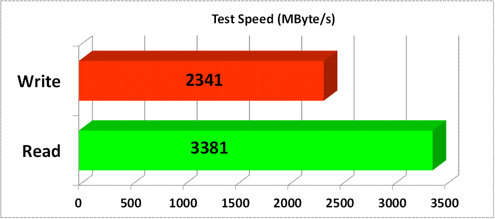
Figure 4‑1 Test Performance of NVMeSW-IP demo by using Samsung 970 Pro SSD
By using PCIe Gen3 on Arria10 GX board, write performance is 2341 Mbyte/sec and read performance is 3381 Mbyte/sec.
5 Revision History
|
Revision |
Date |
Description |
|
1.0 |
30-Apr-2019 |
Initial Release |
|
1.1 |
13-Feb-2020 |
Update header data for All-0 and All-1 pattern |
Copyright: 2019 Design Gateway Co,Ltd.