raNVMe-IP for Gen4 reference design manual
Rev1.0 21-Aug-23
2.2.2 Integrated Block for PCIe
3.1 Test firmware (ranvmeiptest.c)
3.2 Function list in Test firmware
1 Overview
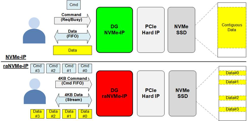
Figure 1‑1 NVMe-IP for Gen4 and raNVMe-IP for Gen4 comparison
NVMe IP Core Series from Design Gateway are the host controller to access the NVMe SSD without integrating CPU or external memory. Many IP solutions are provided to support the different feature. Figure 1‑1 shows the comparison of the features between NVMe-IP and raNVMe-IP.
NVMe-IP is designed for the application that requires the best Write/Read performance of SSD and the data can be stored in contiguous area. The transfer size that is requested by each Write/Read command to NVMe-IP is flexible. The data interface is designed to be FIFO interface. Therefore, user can set large size command to transfer data block to SSD continuously. However, the NVMe-IP is not recommended to the application that stores the data in random addressing, not sequential addressing. The IP is designed to achieve the best performance by using large transfer size, not small transfer size.
raNVMe-IP is the NVMe host controller to support multiple Write or Read commands with 4 Kbyte data size. Each 4 KB data can be stored at the different area of the SSD to support random access. To support multiple commands, the command interface of raNVMe-IP is connected to Cmd FIFO with fixed transfer size to be 4 KB. While the data interface is designed to be Stream interface to transfer 4KB data block for each Write/Read command. Therefore, the raNVMe-IP is fit to the application that uses one SSD to store many data types and each data type is mapped to the different SSD address.
Both NVMe-IP and raNVMe-IP have one user interface. If the application requires multiple user interface, please see more NVMe IP solutions from Design Gateway website.
https://dgway.com/NVMe-IP_X_E.html
2 Hardware overview
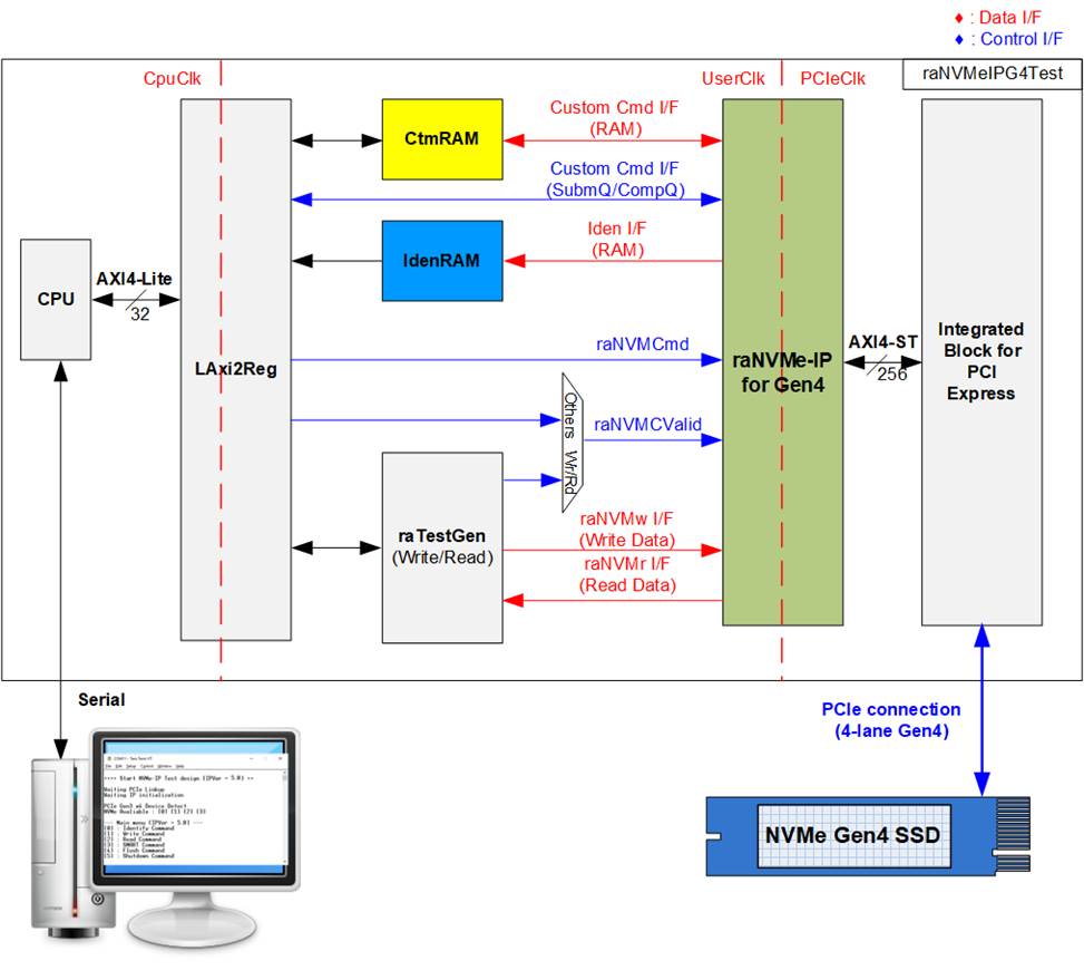
Figure 2‑1 raNVMe-IP for Gen4 demo hardware
Following the function of each module, all hardware modules inside the test system are divided to three types, i.e., test function (raTestGen), NVMe function (CtmRAM, IdenRAM, raNVMe-IP, and PCIe block), and CPU system (CPU and LAxi2Reg).
The command request to raNVMe-IP (raNVMCValid) is created by two modules, depending on the command type. When the command is Single mode (Identify, Shutdown, Flush, or SMART), the command request is generated by CPU firmware via LAxi2Reg. When the command is Multiple mode (Write or Read), the command request is generated by raTestGen module. Also, raTestGen connects to the Data stream interface for transferring the data in Write or Read command. While the received data returned from SSD in SMART command and Identify command are stored to CtmRAM and IdenRAM, respectively.
CPU and LAxi2Reg are designed to interface with user via Serial interface. Therefore, Serial console is applied to receive the test parameters from the user and display the current test status to the user.
There are three clock domains displayed in Figure 2‑1, i.e., CpuClk, UserClk, and PCIeClk. CpuClk is the clock domain of CPU and its peripherals. This clock must be stable clock which may be independent from the clock of other hardware. UserClk is the user clock domain for the user interface of raNVMe-IP. According to raNVMe-IP datasheet, clock frequency of UserClk must be more than or equal to PCIeClk. The reference design uses 275 MHz for UserClk. Finally, PCIeClk is the clock output from PCIe hard IP to synchronous with data stream of 256-bit AXI4 stream bus. When the PCIe hard IP is set to 4-lane PCIe Gen4, PCIeClk frequency is equal to 250 MHz.
More details of the hardware are described as follows.
2.1 raTestGen
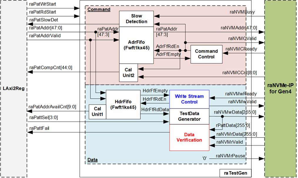
Figure 2‑2 raTestGen Interface
raTestGen is the module to generate command request (raNVMCValid) when the user command is Write or Read command. Also, test pattern for sending or verifying in Write or Read command is created in this module. As shown in Figure 2‑2, the logic inside raTestGen is divided into two parts - Command and Data.
There are the FIFOs inside Command block and Data block - AdrFifo and HdrFifo to store the address which is created by CPU and set via LAxi2Reg. Though 48-bit address is set, only 45-bit address (bit[47:3]) is stored to both AdrFifo and HdrFifo because bit[2:0] is always equal to 000b to align to 4 KB unit. CPU needs to check the free space of the FIFO before writing the new address, read by raPatAddrAvailCnt. The free space size (raPatAddrAvailCnt) is calculated from the data counter of HdrFifo by CalUnit1. To achieve the best performance, the command request and 4 KB data transmission of each command must be controlled parallelly by Command block and Data block, respectively. Generally, there are many commands that are requested to NVMe SSD via raNVMe-IP before starting transferring 4 KB data. Therefore, HdrFifo is always read for operating data path after AdrFifo which is read for generating command request. When calculating the free space size from the data counter of FIFO, the free space size of HdrFifo is always less than AdrFifo. Therefore, it is safe for CPU to check only the free space size of HdrFifo.
The FIFO depth is set to 1024 to be the buffer for storing many command requests from user, created by CPU. If the amount of command in FIFO is much, CPU has more free time to handle other tasks such as displaying the test progress on Serial console while raNVMe-IP is still processing Write/Read command in the FIFO.
Command
To get the best performance for using raNVMe-IP, the new command must be always ready in AdrFifo. Therefore, the CPU firmware is optimized to support random address generating at high-speed rate. However, raPatSlowDet is designed to indicate that AdrFifo has ever been empty while running the latest Write/Read command. If raPatSlowDet is asserted to ‘1’, it means the FIFO has ever been empty and the Write or Read performance cannot show maximum performance because of CPU resource limitation.
The demo shows the Write/Read performance in IOPs unit on the console every second. Therefore, the logic to show total number of completed command is designed. CalUnit2 creates raPatCompCnt which is equal to the total number of commands sent to raNVMe-IP (counted by using AdrFfRdEn signal) subtracted by the number of incomplete commands of raNVMe-IP (raNVMCCnt).
Data
Write Stream Control is the state machine for controlling the data transmission to raNVMe-IP in Write command. One data is read by HdrFifo for generating 4 Kbyte data to raNVMe-IP in each Write command request. The write data enable (raNVMwValid) is asserted to ‘1’ to write the test data to raNVMe-IP. Before sending the data, it needs to check if raNVMe-IP is ready to receive the write data. The details of the state machine are described as follows.
(1) stIdle: In Write command, it waits until HdrFifo has the data (HdrFfEmpty=’0’) for using as 64-bit header data of each 4 Kbyte data. Also, raNVMe-IP must be ready to receive the data by checking raNVMwReady=’1’. After that, HdrFfRdEn is asserted to ‘1’ for one clock cycle to read one data and then 4 Kbyte data is transferred in the next step.
(2) stGenWrData: This state is designed to transfer 4 Kbyte data by asserting raNVMwValid to ‘1’ for 128 clock cycles in Write command. 7-bit counter (rDataCnt) counts the amount of Write data or Read data in each command, controlled by raNVMwValid (Write command) or raNVMrValid (Read command). After finishing transferring 128 data (128x256-bit), continue to the next step.
(3) stDelay: This state adds one clock cycle latency time to wait raNVMwReady updated. After that, it returns to stIdle.
TestData Generator creates test data for sending to raNVMe-IP (raNVMwData) in Write command or verifying with the received data from raNVMe-IP (rPattData) in Read command. The test data of one command is 4-Kbyte size which consists of 64-bit header data and the test pattern, selected by raPattSel. There are five test patterns - all zero, all one, 32-bit incremental data, 32-bit decremental data, and LFSR. All zero and all one pattern are designed by using constant value. While other patterns are designed by separating the data into two parts i.e., 64-bit header and 4088-byte test data for creating unique test data in every 4-Kbyte data, as shown in Figure 2‑3.

Figure 2‑3 Test pattern format of 4096-byte data for Increment/Decrement/LFSR pattern
As shown in Figure 2‑3, 64-bit header in DW#0 and DW#1 is created by using 45-bit address, read from HdrFifo (raPatAddr[47:3]), and then appended zero value to convert the address unit from 4-Kbyte to 512-byte. Remaining data (DW#2 – DW#1023) is the test pattern which can be 32-bit incremental data, 32-bit decremental data, or 32-bit LFSR counter. 32-bit incremental data is designed by using the up-counter. The decremental data can be designed by connecting NOT logic to incremental data. The LFSR pattern uses LFSR counter which has the equation: x^31 + x^21 + x + 1.
To implement 256-bit LFSR pattern, the data is split to be two sets of 128-bit data with assigning different initial value. Each 128-bit data uses look-ahead technique to calculate four 32-bit LFSR data in one clock cycle. As shown Figure 2‑4, the initial value of LFSR is designed by mixing a part of lower 32-bit address (raPatAddr[31:0]) with a part of NOT logic of 32-bit address (raPatAddrB[31:0]).
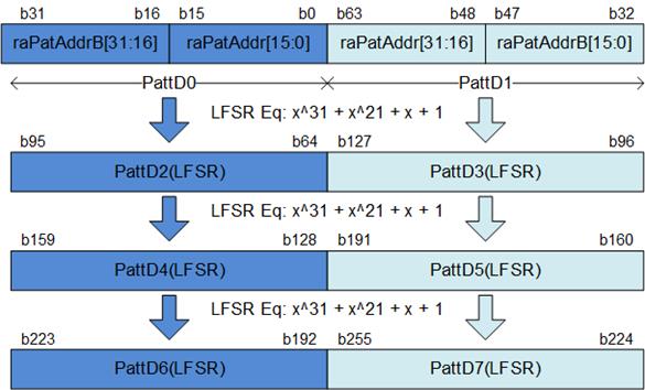
Figure 2‑4 256-bit LFSR Pattern in raTestGen
When the pattern is all zero or all one, there is no 64-bit header inserted to 4Kbyte data
In addition, the user can select test pattern to be all zero or all one data to show the best performance of some SSDs which has data compression algorithm in SSD controller. When the pattern is all zero or all one, there is no 64-bit header inserted to 4-Kbyte data. Some SSDs can show the best performance of Write/Read command when the data is all zero/all one value.
The read operation is controlled without the state machine. The logic is always ready to receive the data from raNVMe-IP by de-asserting raNVMrPause to ‘0’ to get the best Read performance. Therefore, raNVMrValid is always asserted to ‘1’ for 128 clock cycles continuously for transferring 4 KB data of each Read command request. The first data of each 4KB data block is detected by monitoring the rising edge of raNVMrValid and HdrFfRdEn is asserted to ‘1’ for reading the address of the Read command request. TestData Generator is applied to generate the expected data for Read command operation. raPattFail is asserted to ‘1’ when the data verification is failed.
Timing diagram of raTestGen when running Write command and Read command are shown in Figure 2‑5 and Figure 2‑6, respectively.
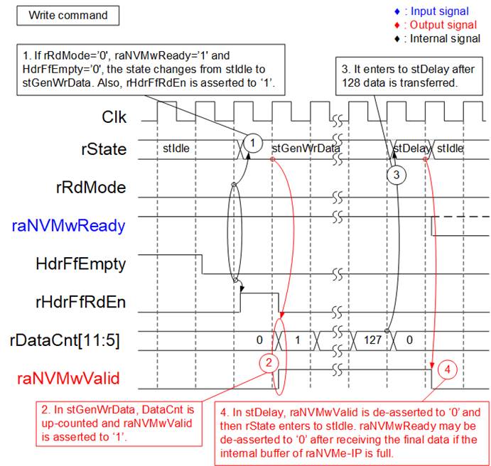
Figure 2‑5 Timing diagram of raTestGen when running Write command
(1) When running Write command (RdMode=’0’), HdrFfEmpty is read to check if the new address is requested by CPU firmware. Also, raNVMwReady is read to check if raNVMe-IP is ready to receive the data. After HdrFfEmpty=’0’ and raNVMwReady=’1’, read enable of HdrFifo (HdrFfRdEn) is asserted to ‘1’ to read one address that is requested by CPU for being the header of each 4 KB data block. After that, it enters to the next state, stGenWrData.
(2) In stGenWrData state, raNVMwValid is asserted to ‘1’ for sending 128 data to raNVMe-IP in Write command. DataCnt is increased to count the amount of transferred data to raNVMe-IP.
(3) After finishing transferring 128 data, monitored by DataCnt, it changes to stDelay.
(4) raNVMwValid is de-asserted to ‘0’ when the state is stDelay. After that, the state enters to stIdle for processing the next command, as described in step 1). After raNVMe-IP receives the last data of each 4 KB, it will check the internal buffer status. raNVMwReady is de-asserted to ‘0’ when the internal buffer of raNVMe-IP is full. Otherwise, raNVMwReady is still asserted to ‘1’ to receive the next 4 KB data block.
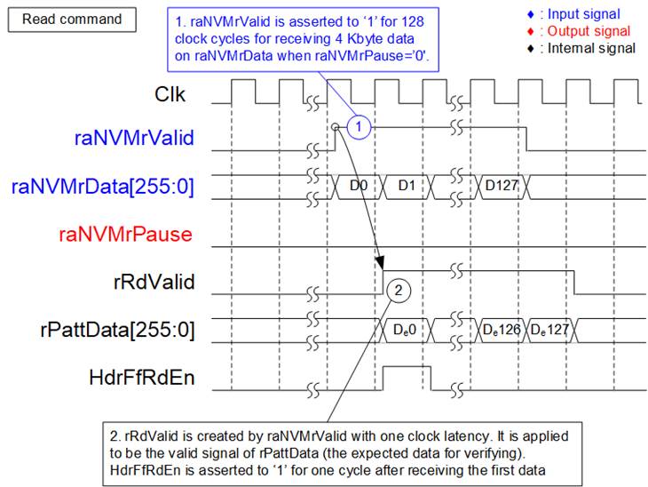
Figure 2‑6 Timing diagram of raTestGen when running Read command
(1) To achieve the best Read performance, raNVMrPause is always de-asserted to ‘0’. Therefore, 4Kbyte read data is returned by raNVMe-IP continuously by asserting raNVMrValid to ‘1’ for 128 clock cycles. The received data is valid on raNVMrData when raNVMrValid is asserted to ‘1’.
(2) When the first data of 4Kbyte data block is received, detected by the rising edge of raNVMrValid, HdrFfRdEn is asserted to ‘1’ to read one address from HdrFifo. The address is applied for creating the header data of 4Kbyte data block. The expected data (De0-De127) is created by TestData Generator to compare with the received data (raNVMrData). rRdValid, created by raNVMrValid with one clock cycle latency, is applied to be the valid signal of Test pattern (rPattData). Also, it is applied to enable the data verification function. To compare data with rPattData, the received data (raNVMrData) must be fed to one Flip-Flop to add one-clock latency for synchronization with rPattData.
2.2 NVMe
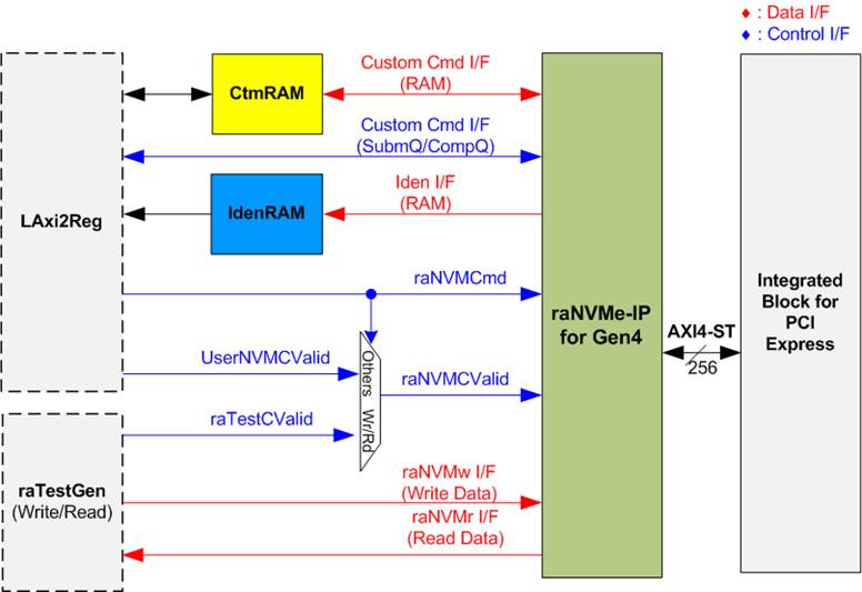
Figure 2‑7 NVMe hardware
Figure 2‑7 shows the interface of raNVMe-IP in the reference design. The user interface of raNVMe-IP consists of Control interface and Data interface. The Control interface receives command and the parameters from the user while Data interface transfers the data when the command needs data transferring.
There are two types of the command, i.e., Single-mode command and Multiple-mode command. The command value (raNVMCmd) is set by CPU firmware via LAxi2Reg, but the command request (raNVMCValid) is controlled by two sources, i.e., UserNVMCValid and raTestCValid. When the command is Single mode, the command request (UserNVMCValid) is created by CPU firmware. When the command is Multiple mode, the command request (raTestCValid) is created by raTestGen. SMART command and Flush command are the Custom commands that need to set the additional parameters via Custom Cmd I/F. In the test design, these parameters are also set by CPU firmware via LAxi2Reg module.
There are four commands which has data transferring by using its own interface.
- Custom Cmd I/F (RAM): Transfer SMART data to CtmRAM in SMART command.
- Iden I/F (RAM): Transfer Identify data to IdenRAM in Identify command.
- raNVMw I/F: Transfer Write data from raTestGen in Write command.
- raNVMr I/F: Transfer Read data from raNVMe-IP in Read command.
Though each command uses the different interface for transferring the data, every data interface has the same data bus size, 256-bit data.
2.2.1 raNVMe-IP for Gen4
The raNVMe-IP implements NVMe protocol of the host side to access one NVMe SSD. Multiple Write or Read commands with random addressing can be sent to raNVMe-IP. Six commands are supported by the IP, i.e., Write, Read, Identify, Shutdown, SMART, and Flush. raNVMe-IP can connect with the PCIe hard IP directly. More details of raNVMe-IP are described in datasheet.
https://dgway.com/products/IP/NVMe-IP/dg_ranvme_ip_data_sheet_g4_xilinx.pdf
2.2.2 Integrated Block for PCIe
This block is the hard IP integrated in some Xilinx FPGAs to support PCIe Gen4 speed. It implements Physical, Data Link, and Transaction Layers of PCIe specification. More details are described in Xilinx document.
PG213: UltraScale+ Devices Integrated Block for PCI Express
https://www.xilinx.com/products/intellectual-property/pcie4-ultrascale-plus.html#documentation
PG343: Versal ACAP Integrated Block for PCI Express
https://www.xilinx.com/products/intellectual-property/pcie-versal.html#documentation
The PCIe hard IP is created by using IP wizard. It is recommended for user to select “PCIe Block Location” which is closed to the transceiver pin that connects to the SSD. Please see more details about the location of PCIe hard IP and transceiver from following document.
UG575: UltraScale and UltraScale+ FPGAs Packaging and Pinouts
https://www.xilinx.com/support/documentation/user_guides/ug575-ultrascale-pkg-pinout.pdf
AM013: Versal ACAP Packaging and Pinouts
https://www.xilinx.com/support/documentation/architecture-manuals/am013-versal-pkg-pinout.pdf
The example of PCIe hard IP location on XCVC1902-VSVA2197 is shown in Figure 2‑8.

Figure 2‑8 PCIe Hard IP Pin location
2.2.3 Dual port RAM
Two dual port RAMs, CtmRAM and IdenRAM, store the returned data from Identify command and SMART command, respectively. IdenRAM has 8 Kbyte size to store 8 Kbyte data, output from Identify command. raNVMe-IP and LAxi2Reg have the different data bus size, 256-bit on raNVMe-IP but 32-bit on LAxi2Reg, so IdenRAM is asymmetric RAM that has the different bus size for Write interface and Read interface. Also, raNVMe-IP has double word enable to write only 32-bit data in some cases. The RAM setting on Xilinx IP tool supports the write byte enable, so the small logic to convert double word enable to be write byte enable is designed as shown in Figure 2‑9.

Figure 2‑9 Byte write enable conversion logic
Bit[0] of WrDWEn with WrEn signal are the inputs to AND logic. The output of AND logic is fed to bit[3:0] of IdenRAM byte write enable. Bit[1], [2], …, [7] of WrDWEn are applied to be bit[7:4], [11:8], …, [31:28] of IdenRAM write byte enable, respectively.
Comparing with IdenRAM, CtmRAM is implemented by true dual-port RAM with byte write enable. The small logic to convert double word enable of Custom interface to be byte write enable must be used, similar to IdenRAM. True dual-port RAM is used to support the additional features when the customized Custom command needs the data input. To support SMART command, using simple dual port RAM is enough. The data size returned from SMART command is 512 bytes.
2.3 CPU and Peripherals
32-bit AXI4-Lite bus is applied to be the bus interface for CPU accessing the peripherals such as Timer and UART. CPU system integrates an additional peripheral to access raNVMe-IP test logic by assigning a unique base address and the address range. Therefore, the hardware logic must be designed to support AXI4-Lite bus standard for CPU writing and reading. LAxi2Reg module is applied to connect with the CPU system via AXI4-Lite bus standard, as shown in Figure 2‑10.
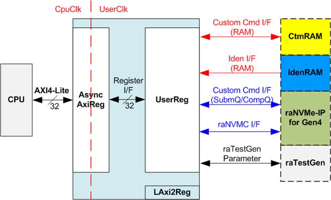
Figure 2‑10 CPU and peripherals hardware
LAxi2Reg consists of AsyncAxiReg and UserReg. AsyncAxiReg is designed to convert the AXI4-Lite signals to be the simple register interface which has 32-bit data bus size, similar to AXI4-Lite data bus size. Besides, AsyncAxiReg includes asynchronous logic to support clock domain crossing between CpuClk and UserClk domain.
UserReg includes the register file of the parameters and the status signals of the modules in raNVMe-IP Test system, i.e., CtmRAM, IdenRAM, raNVMe-IP, and raTestGen. More details of AsyncAxiReg and UserReg are described as follows.
2.3.1 AsyncAxiReg

Figure 2‑11 AsyncAxiReg Interface
The signal on AXI4-Lite bus interface can be split into five groups, i.e., LAxiAw* (Write address channel), LAxiw* (Write data channel), LAxiB* (Write response channel), LAxiAr* (Read address channel), and LAxir* (Read data channel). More details to build custom logic for AXI4-Lite bus is described in following document.
According to AXI4-Lite standard, the write channel and the read channel are operated independently. Also, the control and data interface of each channel are run separately. So, the logic inside AsyncAxiReg to interface with AXI4-Lite bus is split into four groups, i.e., Write control logic, Write data logic, Read control logic, and Read data logic as shown in the left side of Figure 2‑11. Write control I/F and Write data I/F of AXI4-Lite bus are latched and transferred to be Write register interface with clock domain crossing registers. Similarly, Read control I/F of AXI4-Lite bus are latched and transferred to be Read register interface. While the read data is returned from Register interface to AXI4-Lite through clock domain crossing registers. In register interface, RegAddr is shared signal for write and read access, so it loads the value from LAxiAw for write access or LAxiAr for read access.
The simple register interface is compatible with single-port RAM interface for write transaction. The read transaction of the register interface is slightly modified from RAM interface by adding RdReq and RdValid signals for controlling read latency time. The address of register interface is shared for write and read transaction, so user cannot write and read the register at the same time. The timing diagram of the register interface is shown in Figure 2‑12.
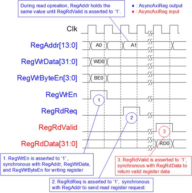
Figure 2‑12 Register interface timing diagram
1) To write register, the timing diagram is similar to single-port RAM interface. RegWrEn is asserted to ‘1’ with the valid signal of RegAddr (Register address in 32-bit unit), RegWrData (write data of the register), and RegWrByteEn (the write byte enable). Byte enable has four bits to be the byte data valid. Bit[0], [1], [2], and [3] are equal to ‘1’ when RegWrData[7:0], [15:8], [23:16], and [31:24] are valid, respectively.
2) To read register, AsyncAxiReg asserts RegRdReq to ’1’ with the valid value of RegAddr. 32-bit data is returned after receiving the read request. The slave detects RegRdReq asserted to start the read transaction. In read operation, the address value (RegAddr) does not change until RegRdValid is asserted to ‘1’. Therefore, the address can be used for selecting the returned data by using multiple layers of multiplexer.
3) The read data is returned on RegRdData bus by the slave with asserting RegRdValid to ‘1’. After that, AsyncAxiReg forwards the read value to LAxir* interface.
2.3.2 UserReg
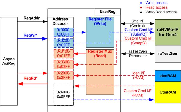
Figure 2‑13 UserReg Interface
The logic inside UserReg consists of Address decoder, RegFile, and RegMux. The address decoder decodes the address which is requested from AsyncAxiReg and then selects the active register for write or read transaction. The address range assigned in UserReg is split into six areas, as shown in Figure 2‑13.
1) 0x0000 – 0x00FF: mapped to set the command with the parameters of raNVMe-IP and raTestGen. This area is write-access only.
2) 0x0200 – 0x02FF: mapped to set the parameters for Custom command interface of raNVMe-IP. This area is write-access only.
3) 0x0100 – 0x01FF: mapped to read the status signals of raNVMe-IP and raTestGen. This area is read-access only.
4) 0x0300 – 0x03FF: mapped to read the status of Custom command interface (raNVMe-IP). This area is read-access only.
5) 0x2000 – 0x3FFF: mapped to Read data from IdenRAM. This area is read-access only.
6) 0x4000 – 0x5FFF: mapped to Write data and Read data with Custom command RAM interface. This area supports write-access and read-access. The demo shows only read access for running SMART command.
Address decoder decodes the upper bit of RegAddr for selecting the active hardware that is raNVMe-IP, raTestGen, IdenRAM, or CtmRAM. The register file inside UserReg is 32-bit bus size. Therefore, write byte enable (RegWrByteEn) is not applied in the test system and the CPU uses 32-bit pointer to set the hardware register.
To read register, multi-level multiplexers (mux) select the data to return to CPU by using the address. The lower bit of RegAddr is fed to the submodule to select the active data from each submodule. While the upper bit is applied in UserReg to select the returned data from each submodule. Totally, the latency time of Read data is equal to three clock cycles. Therefore, RegRdValid is created by RegRdReq with asserting three D Flip-flops. More details of the address mapping within UserReg module are shown in Table 2‑1.
Table 2‑1 Register Map
|
Address |
Register Name |
Description |
|
(Label in the “ranvmeiptest.c”) |
||
|
0x0000 – 0x00FF: Control signals of raNVMe-IP for Gen4 and TestGen (Write access only) |
||
|
BA+0x0000 |
User Address (Low) Reg |
[31:0]: Input to be start address as 512-byte unit (UserAddr[31:0] of raNVMe-IP for Write or Read command) |
|
(USRADRL_INTREG) |
||
|
BA+0x0004 |
User Address (High) Reg |
[15:0]: Input to be start address as 512-byte unit (UserAddr[47:32] of raNVMe-IP for Write or Read command) When writing this register, 48-bit UserAddr is stored to FIFO within raTestGen. |
|
(USRADRH_INTREG) |
||
|
BA+0x0010 |
User Command Reg |
[2:0]: Input to be user command (UserCmd of raNVMe-IP) 000b: Identify, 001b: Shutdown, 010b: Write SSD, 011b: Read SSD, 100b: SMART, 110b: Flush, 101b/111b: Reserved When Single-mode command (not Write/Read) is written to this register, the new command request (raNVMCValid) is asserted to raNVMe-IP. Otherwise, start flag for Write or Read command is asserted to raTestGen. Multi-mode command request (raNVMCValid) is asserted by raTestGen. |
|
(USRCMD_INTREG) |
||
|
BA+0x0014 |
Test Pattern Reg |
[2:0]: Select test pattern. 000b-Increment, 001b-Decrement, 010b-All 0, 011b-All 1, 100b-LFSR. [3]: Verification enable. ‘0’ -No verification, ‘1’-Enable verification. |
|
(PATTSEL_INTREG) |
||
|
BA+0x0020 |
NVMe Timeout Reg |
[31:0]: Timeout value of raNVMe-IP (TimeOutSet[31:0] of raNVMe-IP) |
|
(NVMTIMEOUT_INTREG) |
||
|
0x0100 – 0x01FF: Status signals of raNVMe-IP for Gen4 and TestGen (Read access only) |
||
|
BA+0x0100 |
User Status Reg |
[0]: Mapped to raNVMBusy of raNVMe-IP. ‘0’: IP is Idle, ‘1’: IP is busy. [1]: Mapped to raNVMError of raNVMe-IP. ‘0’: No error, ‘1’: Error is found. [2]: Data verification fail. ‘0’: Normal, ‘1’: Error. [11:4]: Mapped to raNVMCId of raNVMe-IP to show current command ID. [19:12]: Mapped to raNVMDId of raNVMe-IP to show command ID which currently transfers data on Data stream interface. [28:20]: Mapped to raNVMCCnt of raNVMe-IP to show remaining command count stored in raNVMe-IP when running Write or Read command. [31]: Mapped to raNVMCReady of raNVMe-IP to show command ready. |
|
(USRSTS_INTREG) |
||
|
BA+0x0104 |
Total disk size (Low) Reg |
[31:0]: Mapped to LBASize[31:0] of raNVMe-IP |
|
(LBASIZEL_INTREG) |
||
|
BA+0x0108 |
Total disk size (High) Reg |
[15:0]: Mapped to LBASize[47:32] of raNVMe-IP |
|
(LBASIZEH_INTREG) |
||
|
BA+0x010C |
User Error Type Reg |
[31:0]: Mapped to UserErrorType[31:0] of raNVMe-IP to show error status
|
|
(USRERRTYPE_INTREG) |
||
|
BA+0x0110 |
PCIe Status Reg |
[0]: PCIe linkup status from PCIe hard IP (‘0’: No linkup, ’1’: linkup) [3:2]: Two lower bits to show PCIe link speed of PCIe hard IP. MSB is bit[16]. (000b: Not linkup, 001b: PCIe Gen1, 010b: PCIe Gen2, 011b: PCIe Gen3, 111b: PCIe Gen4) [7:4]: PCIe link width status from PCIe hard IP (0001b: 1-lane, 0010b: 2-lane, 0100b: 4-lane, 1000b: 8-lane) [13:8]: Current LTSSM State of PCIe hard IP. Please see more details of LTSSM value in Integrated Block for PCIe datasheet. [16]: The upper bit to show PCIe link speed of PCIe hard IP. Two lower bits are bit[3:2]. |
|
(PCIESTS_INTREG)
|
||
|
NVMe CAP Reg |
[31:0]: Mapped to NVMeCAPReg[31:0] of raNVMe-IP
|
|
|
(NVMCAP_INTREG) |
||
|
BA+0x0118 |
Admin Completion Status Reg |
[15:0]: Mapped to AdmCompStatus[15:0] of raNVMe-IP to show status of Admin completion |
|
(ADMCOMPSTS_INTREG) |
||
|
BA+0x011C |
IO Completion Status Reg |
[31:0]: Mapped to IOCompStatus[15:0] of raNVMe-IP to show status of I/O completion. |
|
(IOCOMPSTS_INTREG) |
||
|
Address |
Register Name |
Description |
|
Rd/Wr |
(Label in the “ranvmeiptest.c”) |
|
|
0x0100 – 0x01FF: Status signals of raNVMe-IP for Gen4 and TestGen (Read access only) |
||
|
BA+0x0120 |
NVMe IP Test pin Reg |
[31:0]: Mapped to TestPin[31:0] of raNVMe-IP |
|
(NVMTESTPIN_INTREG)) |
||
|
BA+0x0124 |
Test FIFO Remaining Count Reg |
[9:0]: Remaining size of FIFO in raTestGen (raPatAddrAvailCnt of raTestGen) |
|
(TESTFFREMCNT_INTREG) |
||
|
BA+0x0128 |
Slow Transfer detect Reg |
[0]: ‘1’-Slow transfer is found, ‘0’-Not detect. It is asserted when CPU firmware sends the address for Write or Read command at slower rate than raNVMe-IP processing. If this flag is asserted to ‘1’, SSD performance result is limited by CPU task. This flag is auto-cleared when CPU sets USRCMD_INTREG=Write or Read command. |
|
(SLOWDET_INTREG) |
||
|
BA+0x0140 |
Data Failure Address(Low) Reg |
[31:0]: Bit[31:0] of the byte address of the 1st failure data in Read command |
|
(RDFAILNOL_INTREG) |
||
|
BA+0x0144 |
Data Failure Address(High) Reg |
[24:0]: Bit[56:32] of the byte address of the 1st failure data in Read command |
|
(RDFAILNOH_INTREG) |
||
|
BA+0x0148 |
Completed Count (Low) Reg |
[31:0]: Bit[31:0] of the number of completed commands in raTestGen (raPatCompCnt of raTestGen) |
|
(CMDCMPCNTL_INTREG) |
||
|
BA+0x014C |
Completed Count (High) Reg |
[12:0]: Bit[44:32] of the number of completed commands in raTestGen (raPatCompCnt of raTestGen) |
|
(CMDCMPCNTH_INTREG) |
||
|
BA+0x0180- BA+0x019F |
Expected value Word0-7 Reg |
256-bit of the expected data at the 1st failure data in Read command 0x0180: Bit[31:0], 0x0184[31:0]: Bit[63:32], …, 0x019C[31:0]: Bit[255:224] |
|
(EXPPATW0-W7_INTREG) |
||
|
BA+0x01C0- BA+0x01DF |
Read value Word0-7 Reg |
256-bit of the read data at the 1st failure data in Read command 0x01C0: Bit[31:0], 0x01C4[31:0]: Bit[63:32], …, 0x01DC[31:0]: Bit[255:224] |
|
(RDPATW0-W7_INTREG) |
||
|
Other interfaces (Custom command of raNVMe-IP for Gen4, IdenRAM, and Custom RAM) |
||
|
BA+0x0200- BA+0x023F |
Custom Submission Queue Reg |
[31:0]: Submission queue entry of SMART and Flush command. Input to be CtmSubmDW0-DW15 of raNVMe-IP. 0x200: DW0, 0x204: DW1, …, 0x23C: DW15 |
|
Wr |
(CTMSUBMQ_STRUCT) |
|
|
BA+0x0300- BA+0x030F |
Custom Completion Queue Reg |
[31:0]: CtmCompDW0-DW3 output from raNVMe-IP. 0x300: DW0, 0x304: DW1, …, 0x30C: DW3 |
|
Rd |
(CTMCOMPQ_STRUCT) |
|
|
BA+0x0800 |
IP Version Reg |
[31:0]: Mapped to IPVersion[31:0] of raNVMe-IP |
|
Rd |
(IPVERSION_INTREG) |
|
|
BA+0x2000- BA+0x2FFF |
Identify Controller Data
|
4Kbyte Identify Controller Data Structure |
|
Rd |
(IDENCTRL_CHARREG) |
|
|
BA+0x3000- BA+0x3FFF |
Identify Namespace Data
|
4Kbyte Identify Namespace Data Structure |
|
Rd |
(IDENNAME_CHARREG) |
|
|
BA+0x4000- BA+0x5FFF |
Custom command RAM
|
Connect to 8K byte CtmRAM interface. Used to store 512-byte data output from SMART Command. |
|
Wr/Rd |
(CTMRAM_CHARREG) |
|
3 CPU Firmware
3.1 Test firmware (ranvmeiptest.c)
After system boot-up, CPU starts the initialization sequence as follows.
1) CPU initializes UART and Timer parameters.
2) CPU waits until PCIe connection links up (PCIESTS_INTREG[0]=’1’).
3) CPU waits until raNVMe-IP completes initialization process (USRSTS_INTREG[0]=’0’). If some errors are found, the process stops with displaying the error message.
4) CPU displays PCIe link status (the number of PCIe lanes and the PCIe speed) by reading PCIESTS_INTREG[16:2].
5) CPU displays the main menu. There are six menus for running six commands of raNVMe-IP, i.e., Identify, Write, Read, SMART, Flush, and Shutdown.
More details for operating each command in CPU firmware are described as follows.
3.1.1 Identify Command
The sequence of the firmware when user selects Identify command is below.
1) Set USRCMD_INTREG=000b to send Identify command request to raNVMe-IP. After that, busy flag (USRSTS_INTREG[0]) changes from ‘0’ to ‘1’.
2) CPU waits until the operation is completed or some errors are found by monitoring USRSTS_INTREG[1:0].
Bit[0] is de-asserted to ‘0’ after finishing operating the command. After that, the data from Identify command of raNVMe-IP is stored in IdenRAM.
Bit[1] is asserted to ‘1’ when some errors are detected. The error message is displayed on the console to show the error details, decoded from USRERRTYPE_INTREG[31:0]. Finally, the process is stopped.
3) After busy flag (USRSTS_INTREG[0]) is de-asserted to ‘0’, CPU displays some information decoded from IdenRAM (IDENCTRL_CHARREG) such as SSD model name and the information from raNVMe-IP output such as SSD capacity (LBASIZEH/L_INTREG). Finally, CPU prepares the polynomial for creating LFSR test pattern following SSD capacity. LFSR test pattern is applied to generate random address for Write command test or Read command test.
3.1.2 Write/Read Command
The sequence of the firmware when user selects Write/Read command is below.
1) Receive transfer mode, data verification (for Read command), start address, transfer length, and test pattern from Serial console. If some inputs are invalid, the operation is cancelled.
Note: Start address and transfer length must be aligned to 8.
2) Get all inputs and set test pattern to PATTSEL_INTREG.
3) Set USRCMD_INTREG[2:0]= 010b for Write command or 011b for Read command.
4) Calculate the maximum address request that can be created. Compare the remaining buffer size to store the address request in the Test logic (TESTFFREMCNT_INTREG[9:0]) with the remaining user request length. The firmware selects the less value.
5) Repeat this step to send the address to the hardware by setting
USRADRL/H_INTREG[31:0] until finishing sending total request. The address value is calculated by using the following rules.
a. If this is the first value of the test, use the Start address received from the user.
b. If transfer mode is Sequential mode, the next address is increased to be the next 4 Kbyte address.
c. If transfer mode is Random mode, calculate the next address by using LFSR equation until the address is not more than SSD capacity.
6) CPU reads error status by reading USRSTS_INTREG[2:1]. Display the error message when some bits are asserted to ‘1’.
Bit[1] is asserted when IP error is detected. After that, error message is displayed on the console to show the error details. Finally, the process is hanged up.
Bit[2] is asserted when data verification is enabled in Read command and data failure is found. After that, the verification error message is displayed. However, CPU is still running until the operation is done or user inputs any keys to cancel operation.
While the command is running, the current transfer size (CMDCMPCNTL/H_INTREG) is read and displayed as percentage every second. Go to the next step (step 7) if remaining total transfer size is equal to 0. Otherwise, return to step 4) to calculate the transfer size for the next loop.
7) CPU waits until raNVMe-IP finishes the operation (USRSTS_INTREG[0]=’0’). Display the error message if some errors are found.
8) Read SLOWDET_INTREG. If the flag is asserted, print the warning message about the performance limitation by CPU firmware. Finally, display the test results on the console, i.e., total time usage, total transfer size, and transfer speed.
3.1.3 SMART Command
The sequence of the firmware when user selects SMART command is below.
1) Set 16-Dword of Submission queue entry (CTMSUBMQ_STRUCT) to be SMART command value.
2) Set USRCMD_INTREG[2:0]=100b to send SMART command request to raNVMe-IP. After that, busy flag (USRSTS_INTREG[0]) changes from ‘0’ to ‘1’.
3) CPU waits until the operation is completed or some errors are found by monitoring USRSTS_INTREG[1:0].
Bit[0] is de-asserted to ‘0’ after finishing operating the command. Next, the data from SMART command of raNVMe-IP is stored in CtmRAM.
Bit[1] is asserted when some errors are detected. The error message is displayed on the console to show the error details, decoded from USRERRTYPE_INTREG[31:0]. Finally, the process is stopped.
4) After busy flag (USRSTS_INTREG[0]) is de-asserted to ‘0’, CPU displays the information which is decoded from CtmRAM (CTMRAM_CHARREG) such as Remaining Life, Percentage Used, Temperature, Total Data Read, Total Data Written, Power On Cycles, Power On Hours, and Number of Unsafe Shutdown.
More details of SMART log are described in NVM Express Specification.
https://nvmexpress.org/resources/specifications/
3.1.4 Flush Command
The sequence of the firmware when user selects Flush command is below.
1) Set 16-Dword of Submission queue entry (CTMSUBMQ_ STRUCT) to be Flush command value.
2) Set USRCMD_INTREG[2:0]=110b to send Flush command request of raNVMe-IP. After that, busy flag (USRSTS_INTREG[0]) changes from ‘0’ to ‘1’.
3) CPU waits until the operation is completed or some errors are found by monitoring USRSTS_INTREG[1:0].
Bit[0] is de-asserted to ‘0’ after finishing operating the command. Next, the CPU returns to the main menu.
Bit[1] is asserted when some errors are detected. The error message is displayed on the console to show the error details, decoded from USRERRTYPE_INTREG[31:0]. Finally, the process is stopped.
3.1.5 Shutdown Command
The sequence of the firmware when user selects Shutdown command is below.
1) Set USRCMD_INTREG[2:0]=001b to send Shutdown command request of raNVMe-IP. After that, busy flag (USRSTS_INTREG[0]) changes from ‘0’ to ‘1’.
2) CPU waits until the operation is completed or some errors are found by monitoring USRSTS_INTREG[1:0].
Bit[0] is de-asserted to ‘0’ after finishing operating the command. After that, the CPU goes to the next step.
Bit[1] is asserted when some errors are detected. The error message is displayed on the console to show the error details, decoded from USRERRTYPE_INTREG[31:0]. Finally, the process is stopped.
3) After Shutdown command is done, the SSD and raNVMe-IP change to inactive status. The CPU cannot receive the new command from user and the user must power off the test system.
3.2 Function list in Test firmware
|
unsigned int cal_lfsr(unsigned int curaddr) |
|
|
Parameters |
curaddr: The latest value of 32-bit address |
|
Return value |
The next value of 32-bit address after finishing LFSR calcalation |
|
Description |
Calculate LFSR value in Write or Read command when running random access mode. |
|
int exec_ctm(unsigned int user_cmd) |
|
|
Parameters |
user_cmd: 4-SMART command, 6-Flush command |
|
Return value |
0: No error, -1: Some errors are found in the raNVMe-IP |
|
Description |
Run SMART command or Flush command, following in topic 3.1.3 (SMART Command) and 3.1.4 (Flush Command). |
|
int get_param(unsigned int user_cmd, userin_struct* userin) |
|
|
Parameters |
user_cmd: 2-Write command, 3-Read command userin: Three inputs from user, i.e., start address, total length in 512-byte unit, and test pattern |
|
Return value |
0: Valid input, -1: Invalid input |
|
Description |
Receive the input parameters from the user and verify the value. When the input is invalid, the function returns -1. Otherwise, all inputs are updated to userin parameter. |
|
void iden_dev(void) |
|
|
Parameters |
None |
|
Return value |
None |
|
Description |
Run Identify command, following in topic 3.1.1 (Identify Command). |
|
int setctm_flush(void) |
|
|
Parameters |
None |
|
Return value |
0: No error, -1: Some errors are found in the raNVMe-IP |
|
Description |
Set Flush command to CTMSUBMQ_STRUCT and call exec_ctm function to operate Flush command. |
|
int setctm_smart(void) |
|
|
Parameters |
None |
|
Return value |
0: No error, -1: Some errors are found in the raNVMe-IP |
|
Description |
Set SMART command to CTMSUBMQ_STRUCT and call exec_ctm function to operate SMART command. Finally, decode and display SMART information on the console |
|
void show_error(void) |
|
|
Parameters |
None |
|
Return value |
None |
|
Description |
Read USRERRTYPE_INTREG, decode the error flag and display error message following the error flag. |
|
void show_pciestat(void) |
|
|
Parameters |
None |
|
Return value |
None |
|
Description |
Read PCIESTS_INTREG until the read value from two read times is stable. After that, display the read value on the console. |
|
void show_result(void) |
|
|
Parameters |
None |
|
Return value |
None |
|
Description |
Print total size by reading CMDCMPCNTL/H_INTREG and then calling show_size function. After that, calculate total time usage from global parameters (timer_val and timer_upper_val) and display in usec, msec, or sec unit. Finally, transfer performance is calculated and displayed on MB/s unit and IOPS unit. |
|
void show_size(unsigned long long size_input) |
|
|
Parameters |
size_input: transfer size to display on the console |
|
Return value |
None |
|
Description |
Calculate and display the input value in MByte, GByte, or TByte unit |
|
void show_smart_hex16byte(volatile unsigned char *char_ptr) |
|
|
Parameters |
*char_ptr: pointer of 16-byte SMART data |
|
Return value |
None |
|
Description |
Display 16-byte SMART data as hexadecimal unit. |
|
void show_smart_int8byte(volatile unsigned char *char_ptr) |
|
|
Parameters |
*char_ptr: pointer of 8-byte SMART data |
|
Return value |
None |
|
Description |
When the input value is less than 4 billion (32-bit), display 8-byte SMART data as decimal unit. Otherwise, display overflow message. |
|
void show_smart_size8byte(volatile unsigned char *char_ptr) |
|
|
Parameters |
*char_ptr: pointer of 8-byte SMART data |
|
Return value |
None |
|
Description |
Display 8-byte SMART data as GB or TB unit. When the input value is more than limit (500 PB), the overflow message is displayed instead. |
|
void show_vererr(void) |
|
|
Parameters |
None |
|
Return value |
None |
|
Description |
Read RDFAILNOL/H_INTREG (error byte address), EXPPATW0-W3_INTREG (expected value), and RDPATW0-W3_INTREG (read value) to display verification error details on the console. |
|
void shutdown_dev(void) |
|
|
Parameters |
None |
|
Return value |
None |
|
Description |
Run Shutdown command, following in topic 3.1.5 (Shutdown Command) |
|
int wrrd_dev(unsigned int user_cmd) |
|
|
Parameters |
user_cmd: 2-Write command, 3-Read command |
|
Return value |
0: No error, -1: Receive invalid input or some errors are found. |
|
Description |
Run Write command or Read command, following in topic 3.1.2 (Write/Read Command). Call wrrd_seq() function when running in sequential mode or wrrd_rand() function when running in random mode. |
|
void wrrd_rand(unsigned int user_cmd, userin_struct* userin) |
|
|
Parameters |
user_cmd: 2-Write command, 3-Read command userin: Three inputs from user, i.e., start address, total length in 512-byte unit and test pattern |
|
Return value |
None |
|
Description |
Run Write command or Read command with 32-bit address calculation in 4 KB unit by using random mode. |
|
void wrrd_seq(unsigned int user_cmd, userin_struct* userin) |
|
|
Parameters |
user_cmd: 2-Write command, 3-Read command userin: Three inputs from user, i.e., start address, total length in 512-byte unit and test pattern |
|
Return value |
None |
|
Description |
Run Write command or Read command with 48-bit address calculation in 512-byte unit by using sequential mode. |
4 Example Test Result
The test results when Command Depth of raNVMe-IP for Gen4 is configured to be 1 Mbyte. The test environment uses 800 GB Intel Optane P5800X and VCK190 board (PCIe Gen4) for running by Random access and Sequential access. The result is shown in Figure 4‑1.

Figure 4‑1 Test Performance of raNVMe-IP for Gen4 demo
The random access uses 4 KB size per command. The result shows 1,410,000 IOPS (5,776 MB/s) for Write command and 1,344,000 IOPS (5,507 MB/s) for Read command. While sequential mode shows almost same performance as random access – 5,862 MB/s for Write command and 5,507 MB/s for Read command. This SSD shows the good performance for both random access and sequential access. However, many SSDs show the less performance when running Random access, comparing to sequential access. Also, many SSDs show the better performance when Command Depth of raNVMe-IP is larger.
5 Revision History
|
Revision |
Date |
Description |
|
1.0 |
11-Jan-23 |
Initial Release |
Copyright: 2023 Design Gateway Co,Ltd.