NVMeTCP-IP for 10G reference design manual
2.1 10G Ethernet System (10G BASE-R)
2.1.2 10G/25G Ethernet MAC Subsystem
2.1.3 Versal Multirate Ethernet MAC
3.1 Test firmware (nvmetcpiptest.c)
3.2 Function list in Test firmware
1 Overview
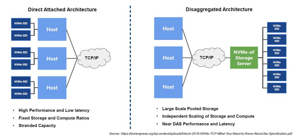
Figure 1‑1 NVMe/TCP vs NVMe-over-PCIe
Traditional storage systems typically employ a direct-attached architecture, where multiple NVMe SSDs are connected to a host via the PCIe interface, adhering to the NVMe over PCIe protocol. As illustrated on the left side of Figure 1‑1, this configuration provides high performance and low latency for data transfers between the storage devices and the host. However, the scalability of these system is limited by the PCIe interface topology, and sharing data across different hosts necessitates an additional network system. The most commonly employed protocol for reliable data transfer over such a network is TCP/IP.
To overcome these limitations, the NVMe/TCP protocol has been developed, as depicted on the right side of Figure 1‑1. NVMe/TCP merges the advanced capabilities of traditional NVMe with the robustness of the TCP/IP protocol, under the standard of NVMe over Fabrics (NVMe-oF). This integration enables a network-based connection, allowing multiple hosts to access multiple SSDs. Such a configuration not only facilitates extensive data sharing across all hosts but also enhances the scalability of storage solutions. By utilizing a network system, NVMe/TCP supports more flexible installation locations for hosts and storage systems, significantly enhancing convenience and ease of maintenance.
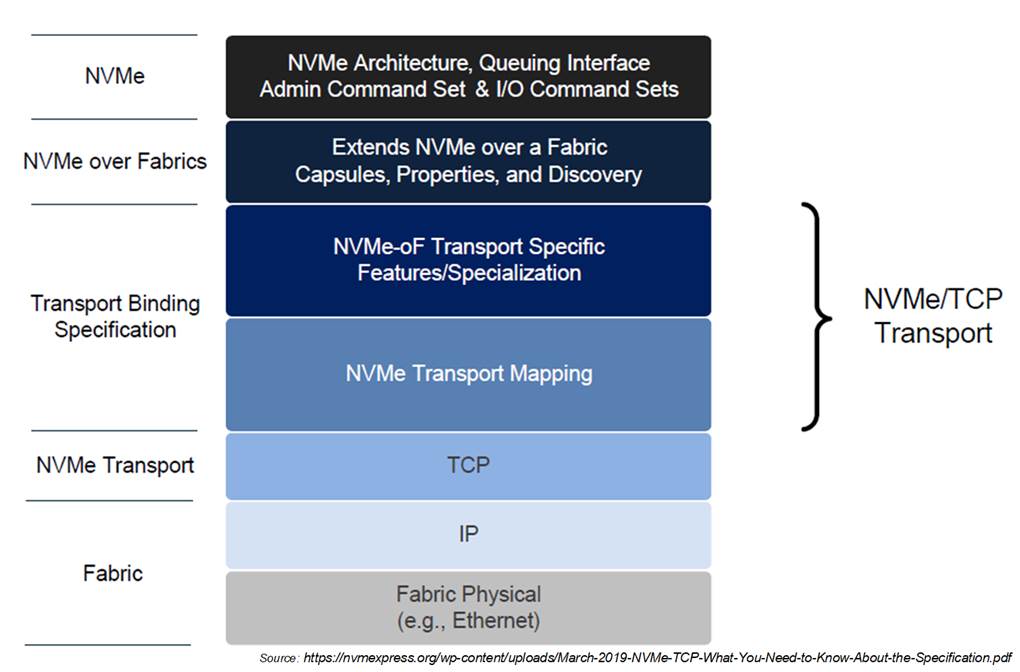
Figure 1‑2 NVMe/TCP protocol layer
As depicted Figure 1‑2, the NVMe/TCP protocol structure incorporates several layers, with the top layer interfacing directly with users. This top layer employs the NVMe protocol to manage command and status interactions for storage access, similar to NVMe over PCIe.
The NVMe/TCP architecture facilitates communication between hosts and storage systems across a network, thereby incorporating an additional protocol layer known as NVMe over Fabrics (NVMe-oF). This layer is crucial for transferring commands, responses, and data using encapsulation methods known as capsules. It also outlines the methodologies for establishing connections between hosts and SSDs within the NVMe subsystem.
NVMe-oF supports various standards including FC-NVMe, RDMA over Converged Ethernet (RoCE), and NVMe/TCP. Figure 1‑3 provides a comparative analysis of these standards. While FC and RoCE offer exceptionally low latency, they require specific network hardware, significantly increasing overall system costs. Conversely, NVMe over TCP (NVMe/TCP) leverages the widely supported TCP/IP protocol, offering lower hardware costs and enhanced flexibility and scalability. However, it is noted that in terms of latency, NVMe/TCP does not perform as well as FC or RoCE.
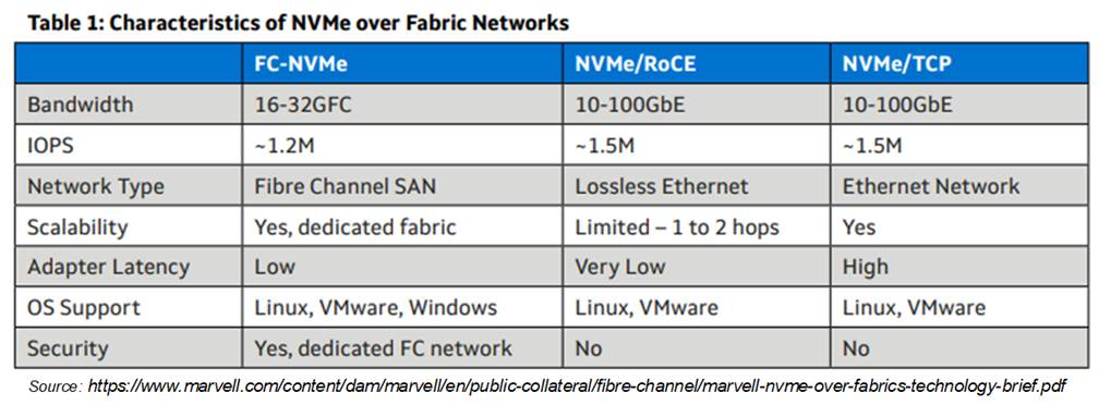
Figure 1‑3 NVMe-oF comparison
For a deeper understanding of the NVMe/TCP protocol, the following documents are recommended.
NVMe Command Set Specification
NVM Express Base Specification
NVM Express TCP Transport Specification
The use of TCP/IP protocol in data transfer across networks ensures reliable data transmission in both directions using a single TCP connection. NVMe/TCP Protocol Data Units (PDUs) can be encapsulated as TCP payloads in one or multiple TCP/IP packets. For more detailed information on the TCP/IP protocol, visit following site.
https://tools.ietf.org/html/rfc793
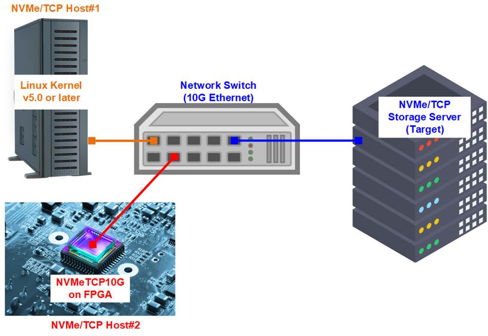
Figure 1‑4 NVMe/TCP Host system
Data transfer using the NVMe/TCP protocol involves two hardware systems: the host and the target. The target system typically functions as a storage server and may incorporate multiple SSDs to achieve high storage capacity. It connects to external systems via network connections such as 10G Ethernet, which facilitates high-speed data access.
Figure 1‑4 illustrates two types of host configuration, Host#1: Server-based implementation and Host#2: FPGA-based implementation. Host#1 is implemented using a server that runs a Linux OS (Kernel version 5.0 or later), which includes support for the NVMe/TCP driver. This setup offers a convenient and flexible hardware arrangement, allowing for easy integration and scalability. However, it is noted that the server’s resource, such as CPU and memory, are shared among various applications. This shared environment can lead to limited and unstable performance due to varying resource demands.
Host#2 utilizes the NVMeTCP10G-IP on an FPGA board. This implementation is dedicated entirely to managing NVMe/TCP operations, which means it operates independently of a CPU or external memory. As a result, this configuration can achieve maximum data transfer rates with greater stability and efficiency. However, it is noted that each NVMeTCP10G-IP instance can access only one SSD at a time. To switch access to a different SSD, the current connection must be terminated first, followed by the establishment of a new connection to the new SSD.
2 Hardware Overview
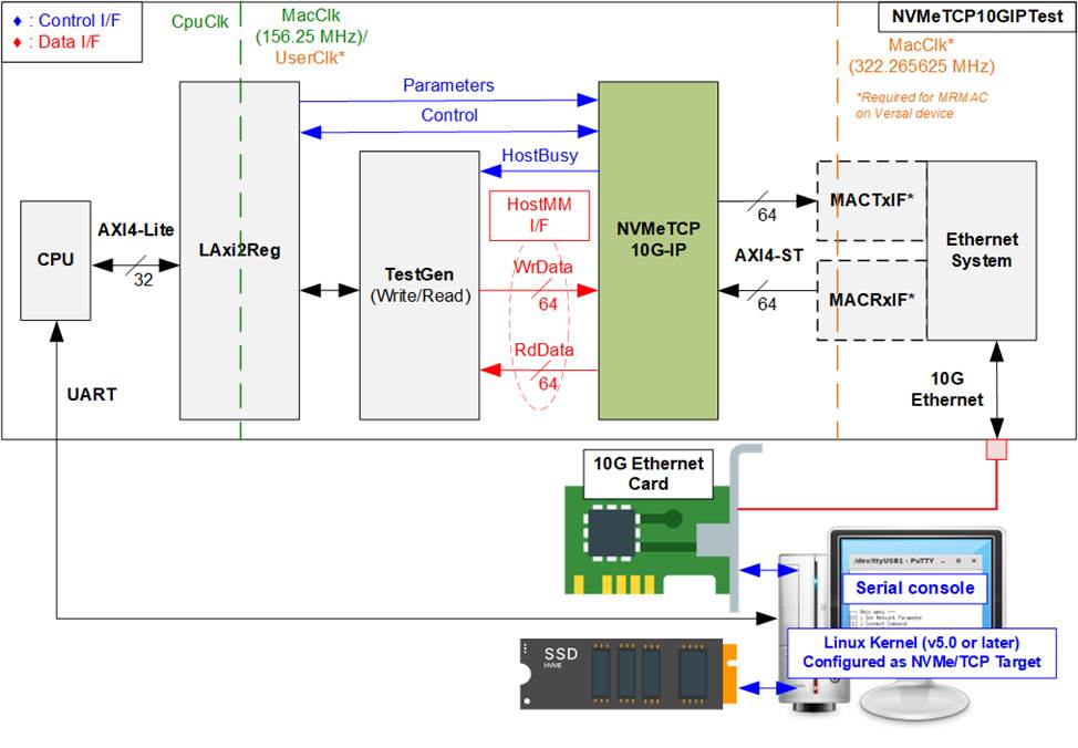
Figure 2‑1 NVMeTCP10G-IP demo hardware
In the test environment, the system comprises two NVMe/TCP set up: a host and a target, interconnected via 10G Ethernet within the same network domain to facilitate system initialization through ARP packet transfers. The host is implemented on an FPGA equipped with the NVMeTCP10G-IP, while the target configuration includes a PC equipped with an NVMe SSD and running Linux Kernel version 5.0 or later, which also supports a 10G Ethernet connection, as depicted in Figure 2‑1.
The NVMeTCP10G-IP is designed to connect to a 10G Ethernet system. This connection can be achieved through various solutions, such as the Multirate Ethernet MAC (MRMAC) on the Versal devices, the 10G/25G Ethernet Subsystem provided by AMD Xilinx, or the DG 10G25GEMAC-IP. Depending on the chosen Ethernet solution, additional adapter logic, such as MACTxIF and MACRxIF, might be required to address any interface mismatches between the NVMeTCP10G-IP and the Ethernet system.
The user interface of the NVMeTCP10G-IP interfaces with two subsystems: the TestGen for initiating Write/Read commands and a processor system for handling connection configurations, parameter setups, and status monitoring.
The TestGen module is connected to the HostMM interface of the NVMeTCP10G-IP, enabling the generation of Write/Read command requests and the data transfers. This module allows users to set test data patterns for Write commands and to verify these patterns during Read operations.
Additionally, the processor system facilitates user configuration of test parameters via a Serial console and enable monitoring of test progress and system status. Command execution sequences are managed through CPU firmware, enhancing user interaction and control over testing procedures.
The reference design generally operates with two clock domains: CpuClk and MacClk, with MacClk typically being sourced from the Ethernet system at 156.25 MHz. In scenarios using MRMAC, the hard IP on Versal devices, the Ethernet system’s clock domain is set to 322.265625 MHz. This setup requires adapter logics, MACTxIF and MACRxIF, to manage seamless data transfer across different clock domains, specifically between MacClk and UserClk. Additionally, the LAxi2Reg module incorporates asynchronous logic to handle clock domain crossings between CpuClk and MacClk/UserClk effectively.
2.1 10G Ethernet System (10G BASE-R)
The 10G Ethernet System integrates multiple layers: the MAC layer, PCS layer, and PMA layer, interfacing with external devices through the 10G BASE-R standard. The Ethernet MAC interface of the NVMeTCP10G-IP utilizes a 64-bit AXI4-stream operating at 156.25 MHz. Adapter logic is required if the NVMeTCP10G-IP interface mismatches the 10G Ethernet system interface.
This reference design explores three Ethernet system implementations: the DG 10G25GEMAC-IP, the 10G/25G Ethernet Subsystem (Soft IP) from AMD Xilinx, and the Multirate Ethernet MAC Subsystem (Hard IP). Details of each solution are provided below.
2.1.1 DG 10G25GEMAC-IP
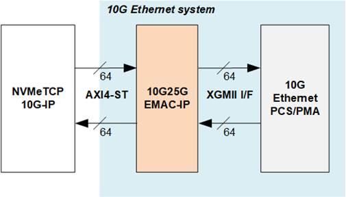
Figure 2‑2 10G Ethernet System by DG 10G25GEMAC
This configuration minimizes FPGA resource utilization by directly connecting with the NVMeTCP10G-IP without the need for additional adapter logics. The 10G Ethernet system encompasses two separate IP cores: the DG 10G25GEMAC-IP and the 10G Ethernet PCS/PMA.
DG 10G25GEMAC-IP
This IP core implements the Ethernet MAC layer using a 64-bit interface at 156.25 MHz, suitable for 10G Ethernet operations. It seamlessly connects between the NVMeTCP10G-IP and the 10G Ethernet PCS/PMA from AMD Xilinx without additional logic. Further details can be found on the Design Gateway website.
https://dgway.com/products/IP/GEMAC-IP/dg_10g25gemacip_data_sheet_xilinx/
10G Ethernet PCS/PMA (10GBASE-R)
This is a no-charge IP core provided by AMD Xilinx, featuring a 64-bit XGMII interface operated at 156.25 MHz designed for 10G speed. More information is available on the AMD Xilinx website.
https://www.xilinx.com/products/intellectual-property/10gbase-r.html
The configuration using IP wizard in this reference design are below.
General/ Select Core : Ethernet PCS/PMA 64-bit
General/ Speed : 10.3125G
PCS/PMA Option/ Base-R/KR Standard : BASE-R
User Interface/ Control and Statistics Interface : Control and Status Vectors
2.1.2 10G/25G Ethernet MAC Subsystem
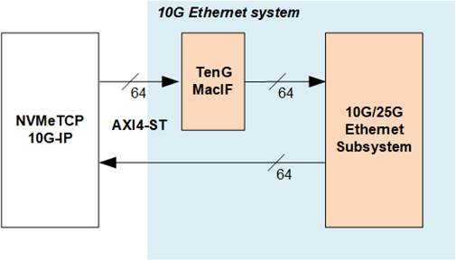
Figure 2‑3 10G Ethernet System by 10G/25G Ethernet MAC Subsystem
The 10G/25G Ethernet MAC Subsystem from AMD Xilinx is an integrated solution that combines a 10G Ethernet MAC with a PCS/PMA in BASE-R mode, specifically designed for use with UltraScale and UltraScale+ FPGAs. While the signal names of the NVMeTCP10G-IP and the 10G/25G Ethernet Subsystem are compatible, there are notable differences in the behavior of the ‘valid’/’ready’ signals within the Transmit interface.
The NVMeTCP10G-IP requires uninterrupted packet transfer from the start to the end of a data packet, necessitating the ‘valid’ and ‘ready’ signals to consistently be asserted to 1b throughout the packet transfer. Conversely, the 10G/25G Ethernet Subsystem may de-assert the ‘ready’ signal, allowing for the pausing of packet transmission before the final data of the packet is transmitted. This necessitates the use of an adapter logic, namely the TenGMacIF, to bridge the NVMeTCP10G-IP and the 10G/25G Ethernet Subsystem.
Further details of the 10G/25G Ethernet MAC Subsystem are available on the AMD Xilinx website.
https://www.xilinx.com/products/intellectual-property/ef-di-25gemac.html
The TenGMacIF serves as an example of adapter logic used in the reference design that incorporates the 10G/25G Ethernet Subsystem. This module, provided by Design Gateway, facilitates compatibility for packet transfer from the NVMeTCP10G-IP to the Ethernet Subsystem. Additional details on this module are described subsequently.
TenGMacIF
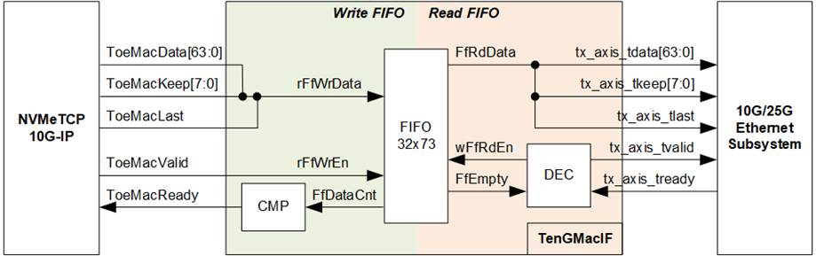
Figure 2‑4 TenGMacIF logic diagram
The 10G/25G Ethernet Subsystem may pause data transmission by de-asserting tx_axis_tready to 0b during packet transfer for brief intervals. To manage these pauses effectively, the TenGMacIF adapter logic includes a small size buffer that can hold 32 of 73-bit data. This FIFO buffers transmitted data from the NVMeTCP10G-IP during the pause periods. The operational logic of TenGMacIF is organized into two groups: Write FIFO and Read FIFO. Below, the functioning of each logic group is explained through a step-by-step process using a timing diagram for clarity.
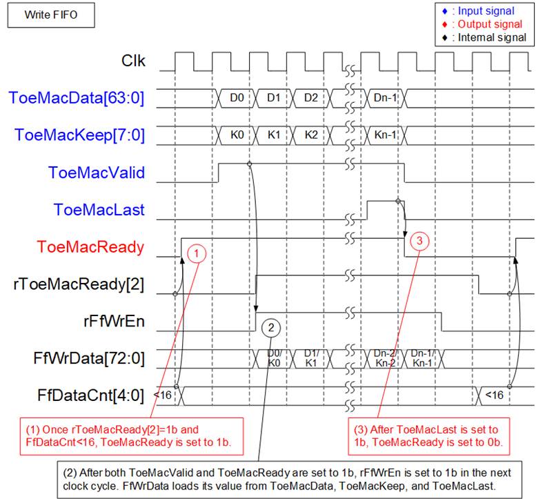
Figure 2‑5 Timing diagram to Write FIFO within TenGMacIF
1) Before initiating a new packet transfer, ensure there is adequate free space in the FIFO. This is indicated when the FfDataCnt value is less than 16. Additionally, verify that the transmission of the previous packet has been completed for more than two clock cycles. This condition is shown by rToeMacReady[2] (a delayed tx_axis_tready by two clock cycles) being set to 0b.
2) During packet transmission, maintain ToeMacValid and ToeMacReady set to 1b to ensure continuous data transmission. One clock cycle after both ToeMacReady and ToeMacValid are set to 1b, set rFfWrEn to 1b to trigger writing new data into the FIFO. The data written into the FIFO consists of the 64-bit data (ToeMacData), an 8-bit of byte enable (ToeMacKeep), and the packet’s last flag (ToeMacLast).
3) When ToeMacLast is set to 1b, indicating the reception of the packet’s last data, de-assert ToeMacReady to 0b for three clock cycles. This pause facilitates the handling and processing of the end-of-packet sequence.
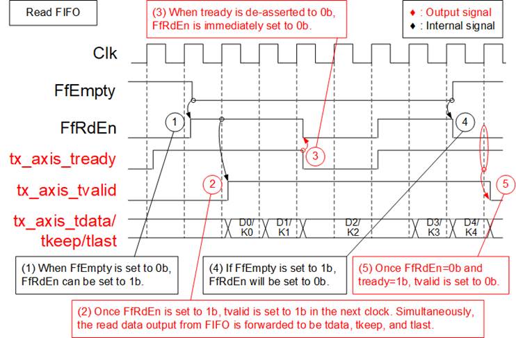
Figure 2‑6 Timing diagram to Read FIFO within TenGMacIF
1) Once the FIFO receives a new packet from the NVMeTCP10G-IP, the empty flag (FfEmpty) is set to 0b, signaling that the data is available in the FIFO. This flag remains at 0b throughout the continuous transmission of the data stream from NVMeTCP10G-IP, until the last data packet is transmitted. To initiate reading the first data of packet from the FIFO, FfRdEn is set to 1b.
2) Set tx_axis_tvalid to 1b to start the data transfer to the 10G/25G Ethernet Subsystem. Simultaneously, the 73-bit read data from the FIFO is divided into 64-bit tx_axis_tdata, 8-bit tx_axis_tkeep, and tx_axis_tast. This process facilitates the continuous transfer of subsequent packet data.
3) If tx_axis_tready is set to 0b during the packet, indicating that the receiving system is not ready to accept more data, FfRdEn must be immediately set to 0b. This action pauses the data transmission and maintains the output values until the receiving system is ready to resume.
4) When the last data of packet has been read from the FIFO, set FfEmpty to 1b and FfRdEn to 0b, indicating that all data of the packet has been successfully transferred from the FIFO.
5) After tx_axis_tready is set to 1b, confirming that the receiving system has successfully accepted the last data, set tx_axis_tvalid to 0b. This change signals the end of the packet transmission.
2.1.3 Versal Multirate Ethernet MAC
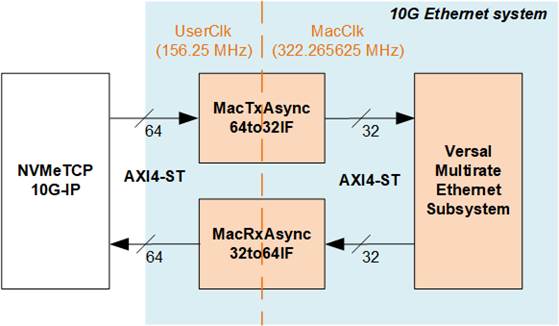
Figure 2‑7 10G Ethernet System by MRMAC
The Multirate Ethernet MAC (MRMAC) is a versatile integrated hard IP that provides both MAC and PHY functionalities for 10G Ethernet operations. Further information of this hard IP can be accessed through the AMD Xilinx website.
https://www.xilinx.com/products/intellectual-property/mrmac.html
MRMAC configuration in the reference design:
MRMAC Configuration Preset : 4x10GE Wide
MRMAC Mode : MAC+PCS
AXI Datapath Interface : Independent 32b Non-Segmented
To bridge the NVMeTCP10G-IP, which uses a 64-bit AXI4-ST interface at 156.25 MHz, with the MRMAC, utilizing a 32-bit AXI4-ST at 322.265625 MHz, specific adapter logics are necessary. These adapters, MACTxAsync64to32IF and MACRxAsync32to64IF, manage clock-crossing domains and facilitate data width conversion, ensuring seamless communication between the NVMeTCP10G-IP and the MRMAC.
MACTxAsync64to32IF
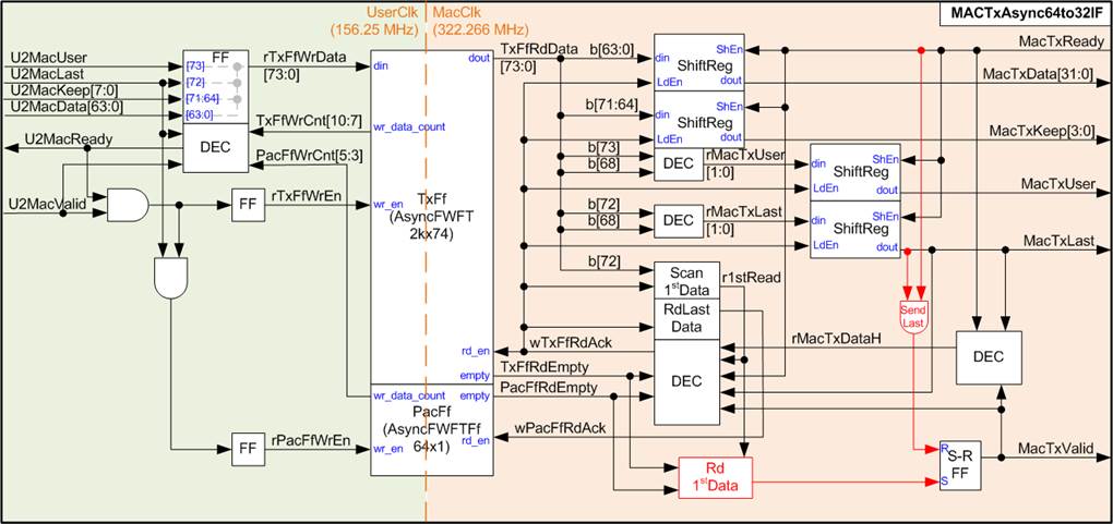
Figure 2‑8 MACTxAsync64to32IF logic diagram
This module enables asynchronous data transfer from a 64-bit AXI4 stream interface (UserClk domain) of the NVMeTCP10G-IP to a 32-bit AXI4 stream interface (MacClk domain) of the Versal Multirate Ethernet Subsystem. It utilizes two First-Word Fall-Through (FWFT) FIFOs to manage the data flow effectively: one FIFO buffers the input stream (TxFf), This setup divides the adpater’s functionality into two primary operations: writing to and reading from the FIFOs.
On the Write side, the UserClk frequency must be at least 156.25 MHz to support the 10G Ethernet transfer rate. As data is transmitted, FIFO may reach capacity, necessitating a pause in the write operation. The write data count of both TxFf and PacFf is monitored to ensure the is adequate space for upcoming packet transfers. If space is insufficient, U2MacReady is de-asserted to 0b, pausing the incoming data stream. To indicate the completion of packet storage in TxFf, dummy data is written to PacFf once the last packet data is stored in TxFf, monitored by U2MacLast being set to 1b.
On the Read side, the operation commences by setting wTxFfRdAck to 1b, initiating the data retrieval from TxFf once all data of one packet is available, monitored by PacFfRdEmpty and TxFfRdEmpty. Reading also depends on there being no remaining data from the previous packet being transferred, indicated by MacTxValid set to 0b, or the successful transfer of the last packet data, indicated by both MacTxReady and MacTxLast set to 1b. Data from TxFf (TxFfRdData) is loaded to shift registers and transmitted to the MRMAC over two clock cycles, converting the 64-bit data into two 32-bit data segments. Data is transferred continuously until the packet is fully transmitted. rMacTxDataH indicates whether the current data transfer strobe to the MRMAC is the lower or the upper 32-bit data set, set to 1b when transmitting the upper 32-bit data set.
The status signal, r1stRead, is set to 1b if the next data read from TxFf is the first data of the packet and 0b otherwise. This signal determines when wTxFfRdAck is asserted to 1b. Once the last data is read from TxFf, wPacFfRdAck is set to 1b for a single clock cycle to clear the dummy data in PacFf.
MacTxValid is controlled by an S-R FF to maintain a value of 1b throughout the packet transfer, asserting at the first data transfer and de-asserting after transferring the last data transfer.
For more illustration, the timing diagram of the Read operation is depicted in Figure 2‑9.
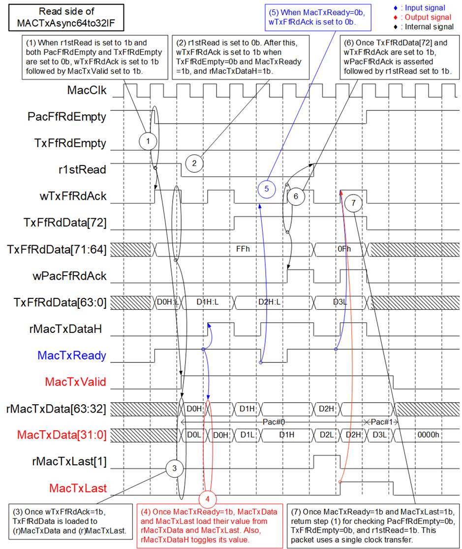
Figure 2‑9 MACTxAsync64to32IF Timing diagram
1) During idle state when MacTxValid is 0b, a new packet transfer can be initiated once all initial conditions are met: r1stRead is set to 1b (indicating the next data is the start of a new packet), and both PacFfRdEmpty and TxFfRdEmpty are 0b (indicating all data of the subsequent packet is available in TxFf). wTxFfRdAck is set to 1b for the first data read, followed by setting MacTxValid to 1b in the subsequent clock cycle, thereby initiating the packet transfer. MacTxValid remains at 1b to ensure continuous transfer all data within the packet until the last data is transmitted.
2) Assume the first packet includes three data (D0, D1, and D2), the last flag (TxFfRdData[72]) remains at 0b for the first two read data cycles. After the first data is read, r1stRead resets to 0b. wTxFfRdAck can be asserted again when there is data in TxFf (TxFfRdEmpty=0b) and after the upper 32-bit data set has been completely transferred (MacTxReady=1b and rMacTxDataH=1b).
3) TxFf is the FWFT type, making the read data (TxFfRdData) immediately valid in the same cycle when wTxFfRdAck is set to 1b. On assertion of wTxFfRdAck, rMacTxData[63:32] and MacTxData[31:0] are loaded from TxFfRdData[63:0]. The last flags for each 32-bit data sets (rMacTxLast[1] and MacTxLast) decodes their values from TxFfRdData[72] (last flag) and TxFfRdData[68] (the flag indicating number of valid bytes for rMacTxData exceeding 4).
4) Once the upper 32-bit data is successfully transferred (MacTxReady=1b), MacTxData and MacTxLast are loaded from rMacTxData[63:32] and rMacTxLast[1], respectively. Additionally, rMacTxDataH toggles to 1b to indicate the current MacTxData is the upper 32-bit of the 64-bit data. This toggle occurs when MacTxReady is set to 1b.
5) If MacTxReady is de-asserted to 0b during a packet transfer, wTxFfRdAck is immediately set to 0b, pausing the data read operation and preserving the current values of MacTxData and MacTxLast.
6) Upon reading the last data from TxFf, as indicated by both wTxFfRdAck and TxFfRdData[72] set to 1b, wPacFfRdAck is set to 1b for a single clock cycle to flush one dummy data from PacFf, decreasing the total packet count in TxFf and resetting r1stRead to 1b, preparing for the first data read of the next packet.
7) Following the successful transmission of the last data (MacTxReady and MacTxLast both set to 1b), and when conditions permit (PacFfRdEmpty and TxFfRdEmpty both set to 0b, r1stRead=1b), a new packet transfer can be initiated, iterating to step 1). wTxFfRdAck is set to 1b during the first data transfer. This new packet contains only 32-bit data, so MacTxLast is set to 1 during the first data transmission, with r1stRead remaining set to 1b following the completion of the first read.
MACRxAsync32to64IF
MacRxAsync32to64IF functions as an adapter for packet transfers from the MRMAC, which operates with a 32-bit AXI4 Stream interface at 322.266 MHz, to the NVMeTCP10G-IP, that utilizes a 64-bit AXI4 Stream interface at 156.25 MHz. This adapter is required for accommodating differences in clock domain and data bus widths between two systems. It includes logic for clock-crossing from the MacClk domain to the UserClk domain and for converting data from 32 bits to 64 bits.
The MRMAC’s output may occasionally pause during any transfer cycle, yet the NVMeTCP10G-IP requires continuous data transfer within each packet. To manage this requirement, the MACRxAsync32to64IF employs an RxFf (FWFT FIFO) to buffer the incoming packet data. This data is first validated by an Error Detection logic.
Additionally, a second FWFT FIFO, PacFf, is utilized to store dummy data marking the end of packet data being written to the RxFf. The FIFO count of PacFf is then used to track and indicate the number of packets stored in RxFf, facilitating data management for retrieval.
As illustrated in Figure 2‑10, the internal logic of the MacRxAsync32to64IF is organized into two groups: the Write FIFO and the Read FIFO. Following explains the details of the Write FIFO and the Read FIFO.
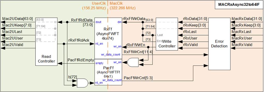
Figure 2‑10 MacRxAsync32to64IF logic diagram
The Error Detection logic continuously monitors the full status of the RxFf and PacFf through their write data counter outputs. If either FIFO approaches the full threshold, the Error Detection logic halts data writing, asserts an error flag, and sets the last flag, indicating that the current has encountered and error. Any remaining data in the packet is then discarded. Data writing resumes only once sufficient space becomes available in both FIFOs and a new packet is received.
The Write Controller manages is responsible for converting data from 32 bits to 64 bits. Typically, the RxFf is written after receiving two 32-bit inputs, except when processing the last packet data. In such cases, if only 32 bits are received, the last data is written to RxFf along with dummy data to maintain alignment. Additionally, the PacFf is written during the last data transfer cycle, signaled when both rRxFfWrEn and rRxFfWrData[72] are set to 1b, marking the end of a data packet.
On the Read side, the process starts by setting rRxFfRdAck to 1b, which initiates the reading of the first data of each packet from RxFf. This action occurs only when all data from one packet is confirmed available in RxFf, as indicated when both PacFfRdEmpty and RxFfRdEmpty are 0b. Once data reading begins, rRxFfRdAck remains asserted until the last packet data is read (marked by RxFfRdData[72]=1b). After reading the last data, rRxFfRdAck is de-asserted for two clock cycles – a specific requirement by NVMeTCP10G-IP for a brief pause following the last packet data. Subsequently, rRxFfRdAck can be re-asserted to 1b once another packet becomes ready for reading.
Detailed operations of the Error Detection and the Write Controller functionalities are depicted in Figure 2‑11 and Figure 2‑12, respectively.
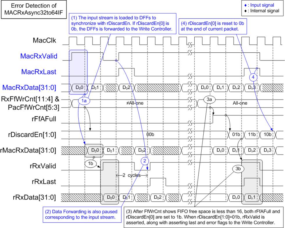
Figure 2‑11 Error Detection of MacRxAsync32to64IF Timing diagram
1) During the Write side operation, the available space in both RxFf and PacFf is continuously monitored using RxFfWrCnt and PacFfWrCnt. In a normal operation scenario, as the input stream is received, it is loaded into to DFFs for synchronization. For example, MacRxData is loaded into rMacRxData. When rDiscardEn[0] is set to 0b, indicating a normal scenario, the data stream from the DFFs is routed to the Write Controller with rRxValid set to 1b, allowing the data stream to proceed.
2) The value of rRxValid is directly related to MacRxValid, and includes a latency time of two clock cycles for transitioning between 1b and 0b. This delay accounts for the necessary synchronization before data can be processed by the Write Controller.
3) If the FIFO space reaches a critical threshold value, both rFfAFull and rDiscardEn[0] are set to 1b. This condition triggers the cessation of the current data stream being forwarded to the Write Controller. Simultaneously, rRxValid, rRxLast, and rRxError are set to 1b, marking the last cycle and indicating an error status of this packet. Following this, the incoming data of the current packet (Dn2 and Dn3) is no longer forwarded to the Write Controller, effectively halting further data processing.
4) Upon detecting the end of the current packet, which is indicated by MacRxLast being set to 1b, the dropped packet function is disabled by de-asserting rDiscardEn[0] to 0b. This action resets the logic to be ready for the next packet, ensuring that the system can return to normal operation without retaining the error state.
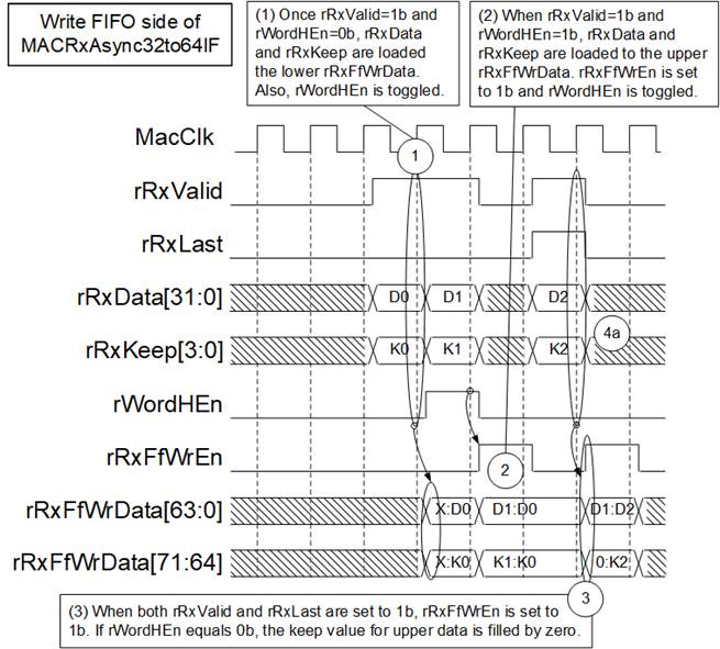
Figure 2‑12 Write Controller of MacRxAsync32to64IF Timing diagram
1) The initial value of rWordHEn, which indicates whether the 32-bit received data is the lower or upper word, is set to 0b at the start of a new packet. Upon receiving new packet data, the first 32-bit data (rRxData[31:0]), along with rRxKeep[3:0] are loaded into the lower data of rRxFfWrData (bits[31:0] and bits[67:64]). rWordHEn is then toggled after each data received, as indicated by rRxValid set to 1b.
2) On the next data cycle where both rWordHEn and rRxValid are set to 1b, the incoming 32-bit data, along with the corresponding control bits, are loaded into the upper data of rRxFfWrData (bits[63:32] and bits [71:68]). During this cycle, rRxFfWrEn is set to 1b, enabling the writing of the complete 64-bit data to the FIFO.
3) When the last data of a packet is received, as indicated by both rRxValid and rRxLast being set to 1b, rRxFfWrEn is always set to 1b to write the data to the FIFO, independent of the state of rWordHEn. If it is determined that only the lower data has been received (rWordHEn=0b), the remaining 4 bits of the Keep value for the upper data are set to zero to ensure alignment. This step guarantees that the data is correctly stored in the FIFO, even when only the lower part of the data is available.
2.2 NVMeTCP-IP for 10G
The NVMeTCP10G-IP serves as a hot controller that enables access to an NVMe SSD in the target system via 10G Ethernet, utilizing the NVMe over TCP protocol. Once a connection is established, the user can issue multiple Write and Read commands until the command queue reaches capacity. Each command transfers a fixed data size of 4 KB. The interface of these commands is a memory-mapped interface (HostMM I/F), which facilitates the transmission of the command along with the 4 KB data block. Detailed specification and further information about the IP can be found on the Design Gateway website.
https://dgway.com/products/IP/NVMeTCP-IP/dg_nvmetcp10g_ip_data_sheet_xilinx/
2.3 TestGen
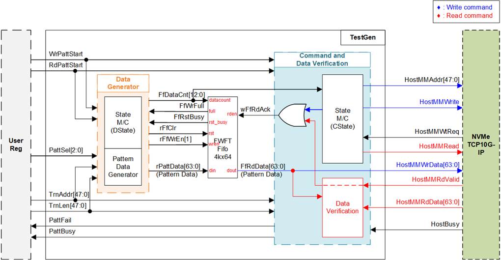
Figure 2‑13 TestGen logic diagram
The TestGen module is a user logic component designed to interface with the NVMeTCP10G-IP, facilitating the generation of commands (HostMMWrite and HostMMRead) and addressing (HostMMAddr) when a user initiates a Write or Read Request (WrPattStart or RdPattStart). It also generates a 4 KB test pattern, which is used for sending or verifying data during Write or Read Commands.
When the NVMeTCP10G-IP is unable to accept additional commands or data, it asserts HostMMWtReq, indicating that it is not ready to proceed. To manage this, TestGen incorporates a FWFTFifo to buffer test data from the Data Generator during such wait times.
TestGen’s logic is categorized into two functional groups to manage the write and read interfaces of FIFO effectively: ‘Data Generator’ and ‘Command and Data Verification’. Data Generator is the component responsible for creating the test data that is temporarily stored in the FWFTFifo. It operates independently, guided by its distinct state (DState), which controls its operations. Command and Data Verification handles the sending of command requests and the transfer of data from the FWFTFifo to the NVMeTCP10G-IP. It operates under its own control state (CState), ensuring efficient management of Write and Read command interface.
The FWFTFifo (FWFT type) stores the test data produced by the Data Generator. During a Write Command, the Command and Verification reads this prepared test data from the FIFO, which is then sent as Write Data (HostMMWrData) through the HostMM interface. Conversely, during a Read Command, Command and Verification waits for Read Data (HostMMRdData) to be returned from the NVMeTCP10G-IP. It then retrieves the prepared test data from the FIFO to verify the accuracy of the received Read Data (HostMMRdData).
Data Generator
The Data Generator component of the TestGen module consists of two main logic groups: a state machine that controls the FIFO write enable (DState), and a Pattern Data Generator that produces the FIFO write data (rPattData). When the user initiates a test by asserting a Write or Read Request (WrPattStart or RdPattStart), the Pattern Data Generator creates test pattern data. This data is then written to the FIFO, managed by the state machine which oversees the flow of data into the FIFO. According to the NVMeTCP10G-IP specification, the data size for a Write or Read Command is fixed at 4 KB, necessitating that the Data Generator writes data in 4 KB bursts to the FIFO, controlled by the Data State Machine (DState). The Data State Machine (DState) operations are detailed below.
1) stDIdle: Awaiting a Write or Read Request from the user (WrPattStart or RdPattStart). Upon activation with test parameters (total transfer size in 512-byte unit: TrnLen, start transfer address in 512-byte units: TrnAddr, and selected test pattern: PattSel), the logic loads the initial values and progresses to the next state: stDRst.
2) stDRst: Asserts a FIFO reset signal (rFfClr) to clear the FIFO before testing begins. This state lasts for one clock cycle.
3) stDWtRst: Waits for the FIFO to be ready for writing post-reset. Once the FIFO is not busy from reset process (FfRstBusy=0b and FfWrFull=0b), it moves to the next step: stDWtFf.
4) stDWtFf: Monitors the FIFO’s available space via the FIFO Data Counter (FfDataCnt). It proceeds to the next state: stDHd once there is sufficient space for 8 KB (two burst sizes).
5) stDHd: Prepare a 64-bit header of each 4 KB data block, using a single clock cycle before proceeding to the next state: stDPatt.
6) stDPatt: Write 4 KB pattern data to the FIFO by asserting the FIFO Write Enable (rFfWrEn) to 1b for 512 clock cycles. The Pattern Data Generator pre-computes the next 64-bit pattern data for subsequent clock cycle. Upon preparing the 511th data pattern, the next state is determined based on several conditions:
a) If it is the last 4 KB of the test (indicated via rPattLenCnt), it transitions back to stDIdle to conclude FIFO writing.
b) If it is not the last 4 KB but the remaining FIFO space is less than 8 KB, it transitions to stDWtFf to complete the current 4 KB and waits for more space.
c) If there is enough space for another 8 KB, it continues to stDHd, allowing for the continuous writing of the next 4 KB data block.
The FIFO has a capacity of 32 KB (supporting eight burst sizes) and pauses writing when available space drops below 8 KB. This design ensures that pattern data is efficiently prepared and stored via the Data State Machine. Once Command and Verification begins reading from the FIFO, the prepared 64-bit pattern data can be read out for at least 512 clock cycles.
A timing diagram illustrating the Data Generator’s streaming write operations to the FIFO in burst mode is shown in Figure 2‑14.
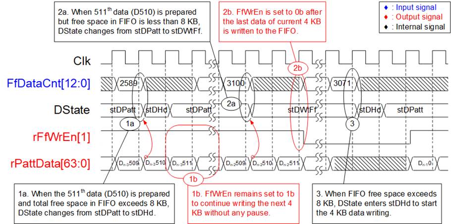
Figure 2‑14 Timing diagram of Data Generator to write pattern data to FIFO
1) Upon completing the preparation of the 511th 64-bit pattern data for the current 4 KB transfer, the Data Generator checks the available FIFO space. If there is more than 8 KB of space available (FfDataCnt<3072), the Data State Machine (DState) progresses to stDHd to continuously write the next 4 KB pattern. This condition is facilitated by keeping rFfWrEn[1] at 1b, enabling the continuation of data writing without interruption.
2) After preparing the 511th 64-bit pattern data for the current 4 KB transfer but the available space is less than 8 KB (FfDataCnt>=3072), DState moves to stDWtFf to pause the FIFO writing. This transition involves setting rFfWrEn[1] to 0b, temporarily halting data input into the FIFO. This pause remains until enough space becomes available to resume operations safely.
3) FIFO writing is resumed once there is sufficient space to accommodate an additional 8 KB (two burst sizes). Maintaining at least 8 KB of free space ensures that the data flow into the FIFO is smooth and uninterrupted, mitigating the risk of overflow.
Command and Data Verification
Command and Data Verification within the TestGen module comprises two main components: a ‘State machine’ (CState) for handling command operations and a ‘Data Verification’ for ensuring data accuracy. This section orchestrates command delivery to the NVMeTCP10G-IP and manages the FIFO’s data during Write or Read operations. The State Machine (CState) operations are detailed below.
1) stCIdle: Waits for a Write or Read Request from the user (WrPattStart or RdPattStart). Upon receiving the request along with the test parameters (transfer size in 512-byte units: TrnLen, start transfer address in 512-byte units: TrnAddr, and selected test pattern: PattSel), these values are loaded and PattBusy is set to 1b, indicating the test is active. Depending on the request type, the start transitions to either stCRdTrn for Read Requests (RdPattStart) or stCWrWt for Write Requests (WrPattStart).
2) stCRdTrn: Handles the sending of Read Command (HostMMRead) to the NVMeTCP10G-IP along with the specified start read address (HostMMAddr) for each 4 KB data segment. After the last Read Command is sent, it transitions to stCWtEnd to wait for the completion of all read operations.
3) stCWrWt: Monitors the FIFO Data Counter (FfDataCnt) and waits until there is at least 4 KB of data available, which is enough to proceed with a write operation.
4) stCWrTrn: Manages the transmission of 4 KB blocks of data from the FIFO as Write Data (HostMMWrData) to the NVMeTCP10G-IP, along with Write Command requests (HostMMWrite). Upon the NVMeTCP10G-IP confirming readiness (HostMMWtReq set to 0b), the FIFO Read Enable (wFfRdAck) is asserted, allowing continuous reading from the FIFO. The FIFO Read Data (FfRdData) directly maps to HostMMWrData for transmission. At the initiation of this state, the first 64-bit HostMMWrData, the address (HostMMAddr), and HostMMWrite are transmitted to the IP. After sending the 511th 64-bit Write Data, proceed to the next state.
5) stCWrChkFf: This state involves sending the last 64-bit HostMMWrData of the current 4 KB block and evaluating the FIFO’s remaining data, monitored by FfDataCnt, to determine the next steps:
a) If this is not the last 4 KB of the Write Command and the FIFO lacks sufficient data for the next block, the state transitions to stCWrWt to await more data from the Data Generator, simultaneously de-asserting the HostMMWrite to 0b.
b) If there is enough data in the FIFO for another round, it returns to stCWrTrn, allowing the next 4 KB block to be sent continuously without de-asserting the HostMMWrite.
c) If the block is the last required by the Write Command (indicated by rMMLenCnt), it moves to stCWtEnd and de-asserts the HostMMWrite to conclude the write operation.
Note: The update latency of the FIFO Data Counter after asserting the FIFO Read Enable requires the threshold value to check for 1-burst-size data availability to be set higher than 4 KB. For simplicity, this threshold is set to 4352 bytes (FfDataCnt=544).
6) stCWtEnd: This final state waits for the completion of either the writing or reading test. It monitors the NVMeTCP10G-IP’s busy flag (HostBusy) with a Flip-Flop. Once HostBusy is observed as 0b, indicating that internal processes have concluded, PattBusy is de-asserted to 0b to signal that the test is completed, and the state returns to stCIdle.
Data Verification is active only during Read tests and operates independently from the CState. It starts once a RdPattStart is asserted and waits for the return of Read Data (HostMMRdData) from the NVMeTCP10G-IP. The Read Data validation signal (HostMMRdValid) acts as the FIFO Read Enable (wFfRdAck), reading pattern data from the FIFO. Each 64-bit HostMMRdData is compared against the expected pattern (FfRdData) to verify accuracy. If a mismatch occurs, PattFail is asserted to notify the user of a verification error.
The timing diagram of Command and Data Verification during Write command execution are illustrated below.
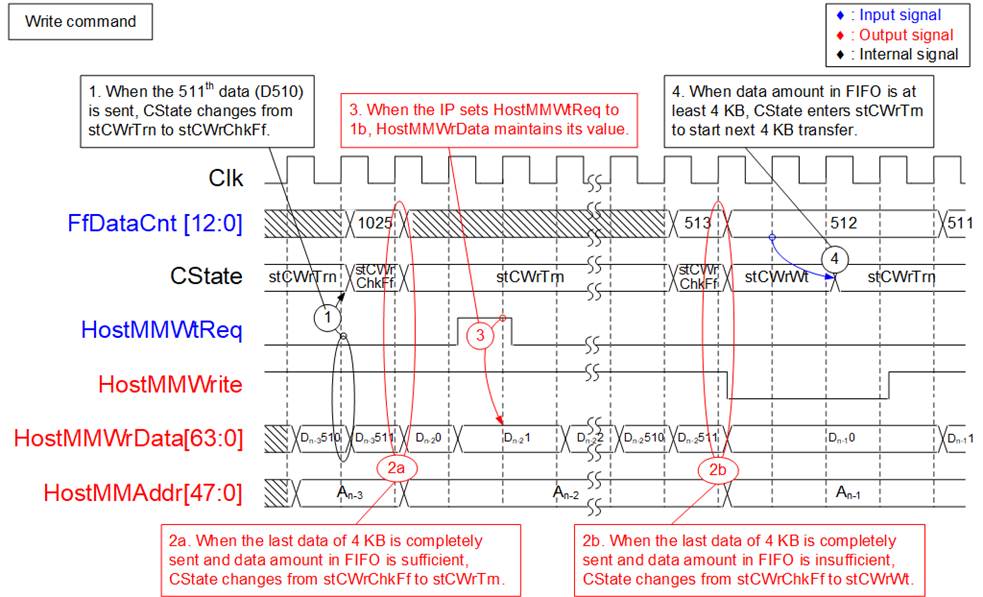
Figure 2‑15 Timing diagram of CState while sending Write command request
1) After transmitting the 511th HostMMWrData (D510) of the 4 KB write transfer, the state machine (CState) enters stCWrChkFf to evaluate conditions for the next 4 KB transfer.
2) In stCWrChkFf, the final HostMMWrData of the current 4 KB write transfer is transmitted. Concurrently, the amount of data remaining in the is assessed to determine the next steps.
a) If the data amount in the FIFO is sufficient (more than 4352 bytes: FfDataCnt>544), CState transitions to stCWrTrn to initiate the next 4 KB write transfer, keeping the HostMMWrite signal asserted to 1b.
b) If there is insufficient data in the FIFO (FfDataCnt≤544), CState moves to stCWrWt to wait for the Data Generator to write the FIFO. During this waiting period, HostMMWrite is set to 0b to signal the completion of the current 4 KB transfer.
3) The NVMeTCP10G-IP acknowledge the receipt of the command and Write data by setting HostMMWtReq to 0b. If it needs to pause the command request or data transmission, HostMMWtReq is set to 1b. During this pause, the value of HostMMWrData must be maintained until HostMMWtReq returns to 0b, indicating readiness to receive more data.
4) Once the 4 KB block is ready in the FIFO, indicated by FfDataCnt≥512, the data transfer resumes by entering stCWrTrn, where the subsequent 4 KB of data is processed and sent.
Figure 2‑16 illustrates the assertion and de-assertion of the PattBusy signal during Write command operations, indicating the TestGen status.
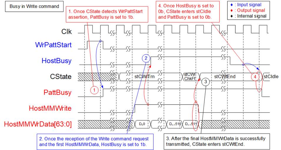
Figure 2‑16 Timing diagram of PattBusy during Write command operation
1) Once the user activates the Write test by setting WrPattStart to 1b, TestGen’s busy flag (PattBusy) is set to 1b. This notifies the user that the operation has started.
2) When the HostMMWrite is set to 1b, which sends the Write command request and the first Write data, the busy flag of the NVMeTCP10G-IP (HostBusy) is also set to 1b, reflecting that the IP is processing the command.
3) After all data has been successfully written to the NVMeTCP10G-IP, CState transitions to stCWtEnd. This state is dedicated to waiting for the NVMeTCP10G-IP to complete the write operation internally.
4) The NVMeTCP10G-IP signifies the end of its processing by setting HostBusy to 0b. Subsequently, PattBusy is de-asserted to 0b, and CState reverts to stCIdle. This de-assertion of PattBusy indicates to the user that the test operation is completed.
The sequence of operations for handling Read commands via the Command and Data Verification during Read command execution are illustrated below.
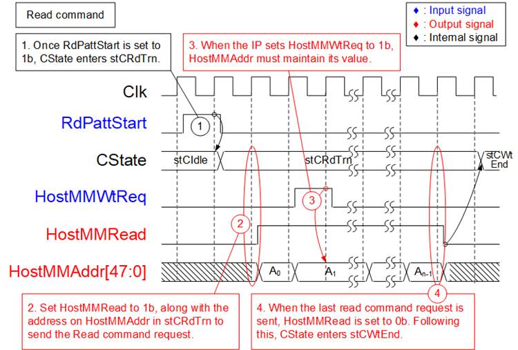
Figure 2‑17 Timing diagram of CState while sending Read command request
1) When the user initiates the Read test by setting RdPattStart, CState transitions to stCRdTrn, marking the beginning of the read operation.
2) Upon entering stCRdTrn, HostMMRead is set to 1b, and the corresponding address for the read operation is assigned to HostMMAddr. To handle multiple Read requests, HostMMRead can be asserted for multiple clock cycles, allowing for several Read commands to be issued sequentially without waiting for completion of previous read data transfers.
3) The NVMeTCP10G-IP acknowledges the receipt of each Read command by setting HostMMWtReq to 0b. If the IP needs to pause the command processing, HostMMWtReq is set to 1b. During such as pause, the value of HostMMAddr must be maintained until HostMMWtReq is reset to 0b, indicating that the IP is ready to receive the next command. This feature allows multiple Read commands to be queued without the need to wait for the 4 KB of read data from preceding commands.
4) After all Read commands have been issued, HostMMRead is reset to 0b. Subsequently, CState transitions to stCWtEnd to await the completion of all operations by the NVMeTCP10G-IP and the return of all requested data.
Figure 2‑18 illustrates the assertion and de-assertion of the PattBusy signal during Read command operations, indicating the TestGen status.

Figure 2‑18 Timing diagram of PattBusy during Read command operation
1) When the user starts the Read test by setting RdPattStart to 1b, TestGen’s busy flag (PattBusy) is asserted to 1b. This action notifies the user that the operation has started.
2) When HostMMRead is activated to send the Read command request to the NVMeTCP10G-IP, the IP’s busy flag (HostBusy) is set to 1b, indicating that the IP is processing the command.
3) Once no further Read commands are to be sent (HostMMRead is set to 0b), CState transitions to stCWtEnd. This state is dedicated to waiting for the completion of all operations within the NVMeTCP10G-IP.
4) For each Read command executed, 4 KB of read data is sequentially returned on HostMMRdData. This data comes with HostMMRdValid set to 1b for 512 clock cycles. The sequence of the returned 4 KB read data aligns with the sequence of the Read commands issued on HostMMRead.
5) Once the NVMeTCP10G-IP has processed all commands and there are no remaining operations in the queue, it sets HostBusy to 0b. Subsequently, PattBusy is de-asserted to 0b, and CState returns to stCIdle. The de-assertion of PattBusy signals to the user that the test operation is fully completed.
Test Data
Test data in TestGen is generated by the Data Generator and used by the Command and Data Verification module either as Write Data (HostMMWrData) or as reference data to verify against Read data (HostMMRdData). Each set of test data for a Command is structured as a 4 KB block, composed of a 64-bit header and a test pattern selected by the user via PattSel.

Figure 2‑19 Test pattern format of 4096-byte data for Increment/Decrement/LFSR pattern
As depicted in Figure 2‑19, the 4 KB data begins with a 64-bit header across DW#0 and DW#1. This header is constructed using a 48-bit address value in 512-byte units corresponding to the physical address of the target SSD. The remainder of the data block (DW#2 – DW#1023) consists of the test pattern, which users can configure in one of three formats: 32-bit incremental data (generated using an up-counter), 32-bit decremental data (created by applying a NOT logic gate to the incremental data), and 32-bit LFSR data. The 32-bit LFSR data utilizes a polynomial equation x^31 + x^21 + x + 1. To ensure efficiency, two 32-bit LFSR outputs are generated in a single clock cycle using look-ahead logic, forming one 64-bit data unit.
Additionally, the user has the option to select test pattern of all zero or all one data. This option is particularly useful for evaluating the performance of SSDs equipped with data compression algorithm in their controllers. When the pattern is set to all zeros or all ones, no 64-bit header is inserted into the 4 KB data block, allowing for straightforward evaluation of compression efficiency.
2.4 CPU and Peripherals
The CPU system uses a 32-bit AXI4-Lite bus as the interface to access peripherals such as the Timer and UART. The system also integrates an additional peripheral to access the test logic by assigning a unique base address and address range. To support CPU read and write operations, the hardware logic must comply with the AXI4-Lite bus standard. LAxi2Reg module, as shown in Figure 2‑20, is designed to connect the CPU system via the AXI4-Lite interface, in compliance with the standard.
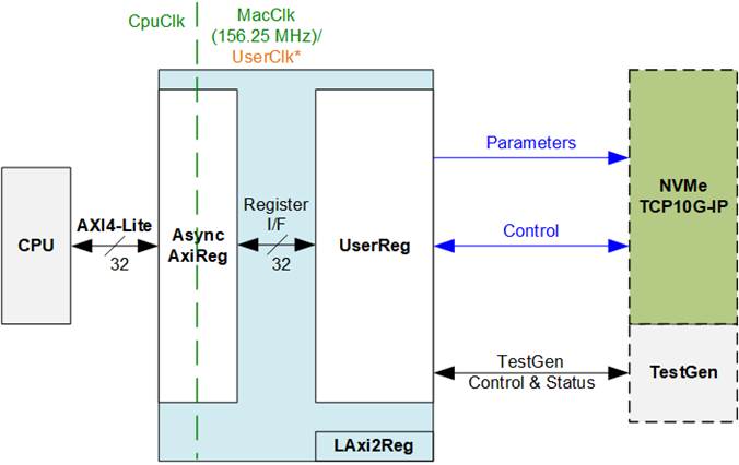
Figure 2‑20 LAxi2Reg block diagram
LAxi2Reg consists of AsyncAxiReg and UserReg. AsyncAxiReg converts AXI4-Lite signals into a simple register interface with a 32-bit data bus size, similar to the AXI4-Lite data bus size. It also includes asynchronous logic to handle clock domain crossing between the CpuClk and MacClk/UserClk domains.
UserReg includes the Register file designed to store parameters and status signals for hardware modules inside the system, including the NVMeTCP10G-IP and TestGen. Additional details regarding AsyncAxiReg and UserReg are provided below.
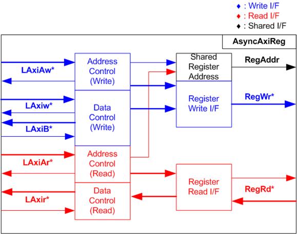
Figure 2‑21 AsyncAxiReg interface
The signal on AXI4-Lite bus interface can be grouped into five groups, i.e., LAxiAw* (Write address channel), LAxiw* (Write data channel), LAxiB* (Write response channel), LAxiAr* (Read address channel), and LAxir* (Read data channel). More details to build custom logic for AXI4-Lite bus is described in following document.
According to AXI4-Lite standard, the write channel and read channel operate independently for both control and data interfaces. Therefore, the logic within AsyncAxiReg to interface with AXI4-Lite bus is divided into four groups, i.e., Write control logic, Write data logic, Read control logic, and Read data logic, as shown in the left side of Figure 2‑21. The Write control I/F and Write data I/F of the AXI4-Lite bus are latched and transferred to become the Write register interface with clock domain crossing registers. Similarly, the Read control I/F of AXI4-Lite bus is latched and transferred to the Read register interface, while Read data is returned from Register interface to AXI4-Lite via clock domain crossing registers. In the Register interface, RegAddr is a shared signal for write and read access, so it loads the value from LAxiAw for write access or LAxiAr for read access.
The Register interface is compatible with single-port RAM interface for write transaction. The read transaction of the Register interface has been slightly modified from RAM interface by adding the RdReq and RdValid signals to control read latency time. The address of Register interface is shared for both write and read transactions, so user cannot write and read the register at the same time. The timing diagram of the Register interface is shown in Figure 2‑22.
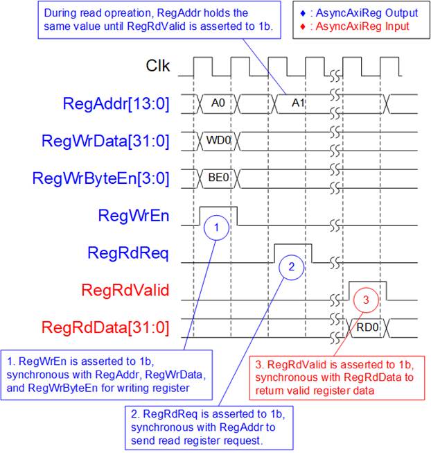
Figure 2‑22 Register interface timing diagram
1) Timing diagram to write register is similar to that of a single-port RAM. The RegWrEn signal is set to 1b, along with a valid RegAddr (Register address in 32-bit units), RegWrData (write data for the register), and RegWrByteEn (write byte enable). The byte enable consists of four bits that indicate the validity of the byte data. For example, bit[0], [1], [2], and [3] are set to 1b when RegWrData[7:0], [15:8], [23:16], and [31:24] are valid, respectively.
2) To read register, AsyncAxiReg sets the RegRdReq signal to 1b with a valid value for RegAddr. The 32-bit data is returned after the read request is received. The slave detects the RegRdReq signal being set to start the read transaction. In the read operation, the address value (RegAddr) remains unchanged until RegRdValid is set to 1b. The address can then be used to select the returned data using multiple layers of multiplexers.
3) The slave returns the read data on RegRdData bus by setting the RegRdValid signal to 1b. After that, AsyncAxiReg forwards the read value to the LAxir* interface.
2.4.2 UserReg
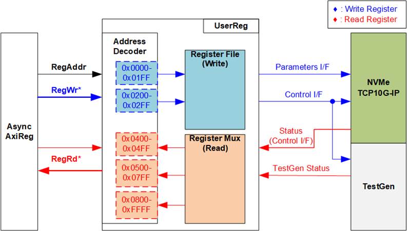
Figure 2‑23 UserReg Interface
The address range for UserReg is organized into five distinct areas, as depicted in Figure 2‑23.
1) 0x0000 – 0x01FF: Allocated for setting parameters specific to the NVMeTCP10G-IP. This area is restricted to write-only operations.
2) 0x0200 – 0x02FF: Allocated for setting control signals for both the NVMeTCP10G-IP and TestGen. Similar to the first area, this area is restricted to write-only operations.
3) 0x0400 – 0x04FF: Allocated for reading status signals from the NVMeTCP10G-IP. This area is restricted for read-only access.
4) 0x0500 – 0x07FF: Allocated for reading status signals of TestGen. This area is also read-only.
5) 0x0800 – 0xFFFF: Allocated for reading the IP version of NVMeTCP10G-IP. This area is read-only.
The Address decoder focuses on the upper bits of RegAddr to selecting the active hardware segment. The internal Register file within UserReg supports a 32-bit bus size. Therefore, the write byte enable (RegWrByteEn) is not utilized in the test system, with the CPU instead employing a 32-bit pointer for setting hardware registers directly.
To read registers, a two-step multiplexing logic is used to select the read data within each address area. The lower bits of RegAddr determine the active register within each area. The upper bits are then decoded to select the corresponding data from the active area, which is subsequently returned to the CPU. The latency for reading data is equal to two clock cycles. To manage this, RegRdValid is generated based on RegRdReq, utilizing two D Flip-flops to ensure the timing alignment and validity of the read data.
Further details of the address mapping within the UserReg module are summarized in Table 2‑1.
Table 2‑1 Register Map
|
Address |
Register Name |
Description |
|
Rd/Wr |
(Label in “nvmetcpiptest.c”) |
|
|
0x0000 – 0x01FF: Parameters of NVMeTCP10G-IP (Write access only) |
||
|
BA+0x0000 |
Host MAC Address (Low) Reg |
[31:0]: Input to be 32 lower bits of the host MAC address. (HostMAC[31:0] of NVMeTCP10G-IP) |
|
(TCP_HML_INTREG) |
||
|
BA+0x0004 |
Host MAC Address (High) Reg |
[15:0]: Input to be 16 upper bits of the host MAC address. (HostMAC[47:32] of NVMeTCP10G-IP) |
|
(TCP_HMH_INTREG) |
||
|
BA+0x0008 |
Host IP Address Reg |
[31:0]: Input to be the host IP address. (HostIPAddr[31:0] of NVMeTCP10G-IP) |
|
(TCP_HIP_INTREG) |
||
|
BA+0x000C |
Host Port Number Reg |
[15:0]: Input to be the host admin port number (HostAdmPort[15:0] of NVMeTCP10G-IP) [31:16]: Input to be the host I/O port number (HostIOPort[15:0] of NVMeTCP10G-IP) |
|
(TCP_HPN_INTREG) |
||
|
BA+0x0010 |
Target IP Address Reg |
[31:0]: Input to be the target IP address. |
|
|
(TCP_TIP_INTREG) |
(TrgIPAddr[31:0] of NVMeTCP10G-IP) |
|
BA+0x0020 |
TCP Timeout Reg |
[31:0]: Input to be TCP timeout value (TCPTimeOutSet[31:0] of NVMeTCP10G-IP) |
|
(TCP_TMO_INTREG) |
||
|
BA+0x0024 |
NVMe Timeout Reg |
[31:0]: Input to be NVMe timeout value (NVMeTimeOutSet[31:0] of NVMeTCP10G-IP) |
|
(NVM_TMO_INTREG) |
||
|
BA+0x0100 - BA+0x010F |
Host NQN Word 0-3 Reg |
Input to be 128-bit NVMe Qualifed Name (NQN) for the host (HostNQN [127:0] of NVMeTCP10G-IP) 0x0100: Bits[31:0], 0x0104: Bits[63:32], …, 0x010C:Bits[127:96] |
|
(HSTNQNW0-W3_INTREG) |
||
|
BA+0x0180 - BA+0x018F |
Target NQN Word 0-3 Reg |
Input to be 128-bit NVMe Qualifed Name (NQN) of the target (TrgNQN[127:0] of NVMeTCP10G-IP) 0x0180: Bits[31:0], 0x0184: Bits[63:32], …, 0x018C:Bits[127:96] |
|
(TRGNQNW0-W3_INTREG) |
||
|
0x00200 – 0x02FF: Control signals of NVMeTCP10G-IP and TestGen (Write access only) |
||
|
BA+0x0200 |
Connection Enable Reg |
[0]: Input to enable the connection with the target (HostConnEn of NVMeTCP10G-IP) |
|
(CONNEN_INTREG) |
||
|
BA+0x0210 |
User Command Reg |
[0]: Input to be command request for writing/reading target SSD 0b: Write SSD , 1b: Read SSD When this register is written, Write or Read command is generated from TestGen to NVMeTCP10G-IP via HostMM interface. |
|
(USRCMD_INTREG) |
||
|
BA+0x0214 |
Test Pattern Reg |
[2:0]: Select test pattern. 000b-Increment, 001b-Decrement, 010b-All 0, 011b-All 1, 100b-LFSR. |
|
(PATTSEL_INTREG) |
||
|
BA+0x0220 |
Host MM Address (Low) Reg |
[31:0]: Input to be 32 lower bits of start address in 512-byte units for the SSD, assigned during Write or Read operation via HostMM interface. |
|
(HMM_ADRL_INTREG) |
||
|
BA+0x0224 |
Host MM Address (High) Reg |
[15:0]: Input to be 16 upper bits of start address in 512-byte units for the SSD, assigned during Write or Read operation via HostMM interface. |
|
(HMM_ADRH_INTREG) |
||
|
BA+0x0228 |
Host MM Length (Low) Reg |
[31:0]: Input to be 32 lower bits of transfer length in 512-byte units for the SSD, assigned during Write or Read operation via HostMM interface. |
|
(HMM_LENL_INTREG) |
||
|
BA+0x022C |
Host MM Length (High) Reg |
[15:0]: Input to be 16 upper bits of transfer length in 512-byte units for the SSD, assigned during Write or Read operation via HostMM interface. |
|
(HMM_LENH_INTREG) |
||
|
Address |
Register Name |
Description |
|
Rd/Wr |
(Label in “nvmetcpiptest.c”) |
|
|
0x0400 – 0x04FF: Status signals of NVMeTCP10G-IP (Read access only) |
||
|
BA+0x0400 |
Host Status Reg |
[0]: Ethernet MAC linkup status. 0b: Ethernet link is not established, 1b: Ethernet Link is established. [1]: Mapped to HostConnStatus of NVMeTCP10G-IP. 0b: NVMe/TCP connection is OFF, 1b: NVMe/TCP connection is ON. [2]: Mapped to HostBusy of NVMeTCP10G-IP. 0b: The IP is Idle, 1b: The IP is busy. [3]: Mapped to HostError of NVMeTCP10G-IP. 0b: No error, 1b: Error is found. [4]: Mapped to PattBusy of TestGen. 0b: Test is Idle, 1b: Test is running. [5]: Mapped to PattFail of TestGen. 0b: No error, 1b: Data Verification fails. |
|
(HSTS_INTREG) |
||
|
Total disk size (Low) Reg |
[31:0]: Mapped to TrgLBASize[31:0] of NVMeTCP10G-IP. |
|
|
(LBASIZEL_INTREG) |
||
|
BA+0x0414 |
Total disk size (High) Reg |
[15:0]: Mapped to TrgLBASize[47:32] of NVMeTCP10G-IP. |
|
(LBASIZEH_INTREG) |
||
|
BA+0x0420 |
Capability (Low) Status Reg |
[31:0]: Mapped to TrgCAPStatus[31:0] of NVMeTCP10G-IP. |
|
(CAPSTSL_INTREG) |
||
|
BA+0x0424 |
Capability (High) Status Reg |
[31:0]: Mapped to TrgCAPStatus[47:32] of NVMeTCP10G-IP. |
|
(CAPSTSL_INTREG) |
||
|
BA+0x0430 |
Host Error Type Reg |
[31:0]: Mapped to HostErrorType[31:0] of NVMeTCP10G-IP to show error status. |
|
(HERRTYPE_INTREG) |
||
|
BA+0x0440 |
NVMe Completion Status Reg |
[15:0]: Mapped to TrgAdmStatus[15:0] of NVMeTCP10G-IP. [31:16]: Mapped to TrgIOStatus[15:0] of NVMeTCP10G-IP. |
|
(NVMCOMPSTS_INTREG) |
||
|
BA+0x0444 |
Admin TCP Status Reg |
[31:0]: Mapped to AdmTCPStatus[31:0] of NVMeTCP10G-IP. |
|
(ADMTCPSTS_INTREG) |
||
|
BA+0x0448 |
IO TCP Status Reg |
[31:0]: Mapped to IOTCPStatus[31:0] of NVMeTCP10G-IP. |
|
(IOTCPSTS_INTREG) |
||
|
BA+0x0450 - BA+0x045F |
Test Pin Word 0-3 Reg |
[31:0]: Mapped to TestPin[127:0] of NVMeTCP10G-IP. 0x0450: Bits[31:0], 0x0454: Bits[63:32], …, 0x045C: Bits[127:96] |
|
(NVMTESTPINW0-W3_INTREG) |
||
|
0x0500 – 0x07FF: Status signals of TestGen (Read access only) |
||
|
BA+0x0500 - BA+0x0507 |
Expected Pattern Word0-1 Reg |
64-bit of the expected data at the 1st failure data in TestGen when operation Read command. 0x0500: Bits[31:0], 0x0504: Bits[63:32] |
|
(EXPPAT0-1_INTREG) |
||
|
BA+0x0540 - BA+0x0547 |
Read Pattern Word0-1 Reg |
64-bit of the read data at the 1st failure data in TestGen when operating Read command. 0x0540: Bits[31:0], 0x0544: Bits[63:32] |
|
(RDPAT0-1_INTREG) |
||
|
BA+0x0580 |
Failure Byte Address (Low) Reg |
[31:0]: Bits[31:0] of the byte address at the 1st failure data in TestGen when operating in Read command. |
|
(RDFAILNOL_INTREG) |
||
|
BA+0x0584 |
Failure Byte Address (High) Reg |
[24:0]: Bits[56:32] of the byte address at the 1st failure data in TestGen when operating in Read command. |
|
(RDFAILNOH_INTREG) |
||
|
BA+0x0590 |
Current Test Byte (Low) Reg |
[31:0]: Bits[31:0] of the current test data size in bytes of TestGen when operating in Write or Read command. |
|
(CURSIZEL_INTREG) |
||
|
BA+0x0594 |
Current Test Byte (High) Reg |
[24:0]: Bits[56:32] of the current test data size in bytes of TestGen when operating in Write or Read command. |
|
(CURSIZEH_INTREG) |
||
|
0x0800 – 0xFFFF: Other interfaces |
||
|
BA+0x0800 |
IP Version REG |
[31:0]: Mapped to IPVersion[31:0] of NVMeTCP10G-IP |
|
Rd |
(IPVERSION_INTREG) |
|
|
BA+0x0804 |
EMAC Version REG |
[31:0]: Mapped to IPVersion[31:0] of Ethernet MAC-IP from Design Gateway. Assigned by zero for other IP vendors. |
|
Rd |
(EMACVERSION_INTREG) |
|
3 CPU Firmware
3.1 Test firmware (nvmetcpiptest.c)
Upon system boot-up, the CPU initiates by configuring UART and Timer settings. It then begins polling the 10G Ethernet link up status, specifically monitoring the HSTS_INTREG[0]. The CPU continues to poll this register until the Ethernet link is established, at which point it displays the main menu on Serial console.
The main menu offers five test operations for user interaction: Set Network Parameter, Connect, Write Command, Read Command, and Disconnect. There are some restrictions for executing each test operations, described as below.
1) The user must start by setting the network parameters as the initial step.
2) Next, the user should choose to ‘Connect’ option to establish a connection with the target SSD.
3) Once the connection is established, the user has the option to perform Write or Read operations on the target SSD.
4) To terminate the connection with the target SSD, the user selects ‘Disconnect’ option.
5) After disconnecting, the user can return to setting network parameters or reconnect by selecting ‘Connect’ option again.
Note: If reconnecting to the same target SSD, re-setting the network parameters can be skipped.
The main menu dynamically displays only the appropriate options based on the current state of the system. If a user selects an option that is not currently available or displayed on the Serial console, no action will be taken.
3.1.1 Set Network Parameter
This menu facilitates the configuration of network parameters necessary for initializing the NVMeTCP10G-IP, including the Host MAC address, Host IP address, Host port numbers, Target IP address, and the NVMe Qualified Name (NQN) of both the host and the target. The step-by-step procedure for setting these parameters is as follows.
1) The console displays the current parameter values. If parameters are not previously set, default values defined in the firmware are shown.
2) The user is prompted to either confirm the current parameters or input new values.
a) Press ‘x’ on the keyboard to skip and retain current settings.
b) Press any other key to proceed with entering new parameter values.
3) If the user opts to set new value (any key other than ‘x’), they are prompted to input the following parameters: Target NQN, Host MAC address, Host IP address, Host port numbers (Admin and I/O ports), and Target IP address. If an input is invalid, the system retains the most recent valid value for that parameter.
4) Once the parameters are set (or if the ‘x’ key is pressed to skip), the CPU registers these values into the following parameter registers: TRGNQNW0-3_INTREG, HSTNQNW0-3_INTREG, TCP_HML/H_INTREG, TCP_HIP_INTREG, TCP_HPN_ INTREG, TCP_TIP_INTREG, TCP_TMO_INTREG, and NVM_TMO_INTREG).
Note: Some values are always set to defaults by the firmware:
· TCP timeout value : 1 second
· NVMe timeout value : 4 seconds
· Host NQN : “dgnvmehtest”
3.1.2 Connect
This menu facilitates establishing a connection between the NVMeTCP10G-IP (the host) and the target system, which is a prerequisite for executing Write or Read commands on the target SSD. The process for establishing this connection is outlined below.
1) The connection enable flag (CONNEN_INTREG[0]) is set to 1b to start the connection process.
2) The CPU continuously monitors HSTS_INTREG[3:0] to check the status and detect any errors during the connect process.
· Bit[0]: De-asserted to 0b if the ethernet connection is lost. The error message is then displayed, and the process is halted.
· Bit[1]: Asserted to 1b when connection status is established. The process then waits for bit[2] to be de-asserted, confirming the completion of the command operation before proceeding.
· Bit[3]: Asserted to 1b if an error is detected. The error message is then displayed, and the process is halted.
3) Once a connection is successfully established, the capacity of the target SSD is retrieved and displayed in GB, using the registers 'LBASIZEL/H_INTREG'.
3.1.3 Write/Read Command
These menus enable the testing of NVMeTCP10G-IP by facilitating data write and read operations to and from the target SSD. The sequence of executing these commands is as follows.
1) The user inputs the start address, transfer length, and test pattern. All inputs must be valid to proceed; otherwise, the operation is cancelled.
Note: Because Write or Read command data size is fixed to 4 KB, both the start address and transfer length (in 512-byte units) must be aligned to 8.
2) After collecting all inputs, they are set in the respective registers: HMM_ADRL/H_ INTREG for address, HMM_LENL/H_INTREG for length, and PATTSEL_INTREG for the selected test pattern.
3) Set USRCMD_INTREG[0] based on the command type (0b for Write, 1b for Read). Following this setting, the Test logic (TestGen) generates the appropriate command via the HostMM I/F to NVMeTCP10G-IP. Concurrently, the test busy flag (HSTS_INTREG[4]) transitions from 0b to 1b, indicating that the IP has begun processing the command.
4) The CPU continuously monitors HSTS_INTREG[5:3] and HSTS_INTREG[0] to detect completion or errors during the operation.
· Bit[0]: De-asserted to 0b if the ethernet connection is lost. The error message is then displayed, and the process is halted.
· Bit[3]: Asserted to 1b if an error is detected. The error message is then displayed, and the process is halted.
· Bit[4]: De-asserted to 0b when the command operation is completed, indicating that both NVMeTCP10G-IP and TestGen have returned to idle status.
· Bit[5]: Asserted to 1b if data verification fails. The verification error message is displayed, but the CPU continues running until the operation concludes or a user enters any key on the console to cancel the operation.
During the command execution, the current amount of transferred data (read from CURSIZEL/H_INTREG) is displayed every second to inform the user of progress.
5) Once the test busy flag (HSTS_INTREG[4]) is de-asserted to 0b, the CPU summarizes and displays the test result on the console, including total time used, total transfer size, and transfer speed.
3.1.4 Disconnect
This menu facilitates the termination of existing TCP and NVMe/TCP connections between the host and the target, which were previously established via the ‘Connect’ command. The sequence for disconnecting is outlined as follows.
1) The connection enable flag (CONNEN_INTREG[0]) is reset to 0b, signaling the start of the disconnection process.
2) The CPU continuously monitors HSTS_INTREG[3:0] to check the status and detect any errors during the disconnect process.
· Bit[0]: De-asserted to 0b if the ethernet connection is lost. The error message is then displayed, and the process is halted.
· Bit[1]: Asserted to 0b when connection status is disconnected. The process then waits for bit[2] to be de-asserted, confirming the completion of the command operation before proceeding.
· Bit[3]: Asserted to 1b if an error is detected. The error message is then displayed, and the process is halted.
3) The user has the option to reconnect to the same target using the ‘Connect’ command without needing to reset the network parameters. If a connection to a new target is desired, it is necessary to first select “Set Network Parameter” to configure the appropriate settings for the new target.
3.2 Function list in Test firmware
|
void error_handler(void) |
|
|
Parameters |
None |
|
Return value |
None |
|
Description |
This function is invoked when an error occurs within the system. By default, the function is designed to enter and infinite loop, effectively halting further execution. Users can modify this function to implement error handling operations tailored to their specific needs. |
|
unsigned long long get_cursize(void) |
|
|
Parameters |
None |
|
Return value |
Read value of CURSIZEL/H_INTREG |
|
Description |
Read the CURSIZEL/H_INTREG register and return the read value. It is used to monitor the current size of the data that has been processed. |
|
int get_param(userin_struct* userin) |
|
|
Parameters |
userin: This structure includes three user inputs: start address, total transfer length in 512-byte units, and test pattern. |
|
Return value |
STATUS_SUCCESS: Operation is success. STATUS_INVALIDINPUT: Receive an invalid input. |
|
Description |
Receive input parameters from the user and verify their validity. Valid inputs are updated in the userin parameter structure. If any input is invalid, the function returns -1 and does not update the parameters. |
|
void get_string(unsigned char* out_val) |
|
|
Parameters |
out_val: A character array intended to store a 16-byte NQN |
|
Return value |
None |
|
Description |
Receive a string from the user to assign the NQN value. Users finalize their input by pressing the ‘Enter’ key. This function accommodates a maximum of 16 characters. If the entered string is shorter than 16 characters, the remaining characters are filled with ‘00h’ (Null). |
|
int proc_connect(void) |
|
|
Parameters |
None |
|
Return value |
STATUS_SUCCESS: Operation is success. STATUS_ETHDOWN: Ethernet link is down. STATUS_ERROR: An error is found. |
|
Description |
This function implements the ‘Connect’ operation as detailed in section 3.1.2. It establishes a connection between the NVMeTCP10G-IP and the target system. |
|
int proc_disconnect(void) |
|
|
Parameters |
None |
|
Return value |
STATUS_SUCCESS: Operation is success. STATUS_ETHDOWN: Ethernet link is down. STATUS_ERROR: An error is found. |
|
Description |
Execute the ‘Disconnect’ operation as described in section 3.1.4. This function terminates the existing connections between the host and the target system. |
|
int set_netparam(void) |
|
|
Parameters |
None |
|
Return value |
STATUS_SUCCESS: Operation is success. STATUS_INVALIDINPUT: Receive an invalid input. |
|
Description |
Execute the ‘Set Network Parameter’ operation according to the guidelines in section 3.1.1. This function prompts the user to enter network settings, verifies the validity of the inputs, and applies the configurations if they are valid. |
|
void set_param(void) |
|
|
Parameters |
None |
|
Return value |
None |
|
Description |
A supported function used by ‘set_netparam’ to configure hardware registers. It utilizes the parameters previously assigned by users during the network setting process (referenced in step 4 of section 3.1.1) . |
|
void show_error(void) |
|
|
Parameters |
None |
|
Return value |
None |
|
Description |
This function reads the error type from HERRTYPE_INTREG, decode the error flags, and display a corresponding error message. Specific error types may trigger additional reads to provide more detailed information. · If bit[2]=1b, it reads CAPSTSL/H_INTREG to display SSD information. · If bit[10]/[18]=1b, it reads NVMCOMPSTS_INTREG to display the NVMe completion entry status. · If bit[15]=1b, it reads ADMTCPSTS_INTREG to display the TCP status of the Admin port. · If bit[23]=1b, it reads IOTCPSTS_INTREG to display the TCP status of the IO port. Additionally, it calls ‘show_testpin’ to display the value of internal IP test pins. |
|
void show_param(void) |
|
|
Parameters |
None |
|
Return value |
None |
|
Description |
Display the current network parameters by reading from global settings. Parameters shown include Host NQN, Target NQN, Host MAC address, Host IP address, Host port numbers (Admin and IO), and Target IP address. |
|
void show_result(void) |
|
|
Parameters |
None |
|
Return value |
None |
|
Description |
Print the total data size processed using the ‘get_cursize’ and ‘show_size’ functions. It calculates the total time used from global timer parameters (timer_val and timer_upper_val) and displays it in usec, msec, or sec units. Lastly, it calculates and displays the data transfer performance in MB/s. |
|
void show_size(unsigned long long size_input) |
|
|
Parameters |
size_input: the transfer size to be displayed on the console |
|
Return value |
None |
|
Description |
Convert and display the input value in MB or GB units. |
|
void show_testpin(void) |
|
|
Parameters |
None |
|
Return value |
None |
|
Description |
Read NVMTESTPINW0-3_INTREG and display the IP test pins on the console. This function is particularly useful for debugging purposes. |
|
void show_vererr(void) |
|
|
Parameters |
None |
|
Return value |
None |
|
Description |
This function is responsible for displaying detailed error information regarding data verification failures. It reads from the following registers: RDFAILNOL/H_INTREG (shows the address where the error occurred), EXPPAT0-1_INTREG (shows the expected data value), and RDPAT0-1_INTREG (shows the actual read data value). |
|
void wait_ethlink(void) |
|
|
Parameters |
None |
|
Return value |
None |
|
Description |
Monitor the Ethernet link up status by reading HSTS_INTREG[0]. The function will loop until the Ethernet link is successfully established. |
|
int wrrd_dev(unsigned int user_cmd) |
|
|
Parameters |
user_cmd: 0-Write command, 1-Read command, |
|
Return value |
STATUS_SUCCESS: Operation is success. STATUS_ETHDOWN: Ethernet link is down. STATUS_ERROR: An error is found. STATUS_VERFAIL: User cancels operation after data verification fails. STATUS_INVALIDINPUT: Receive invalid input. |
|
Description |
Execute the ‘Write’ or ‘Read’ operation according to the process described in section 3.1.3. This function handles user commands to interact with the NVMeTCP10G-IP, directing operation to write to or read from the target SSD depending on the user’s input. |
4 Example Test Result
This demo uses the NVMeTCP10G-IP hosted on a KCU105 board, with a 512 GB Samsung 960 Pro SSD installed in a target PC running Linux OS, kernel version 5.4.0-81. The results are illustrated in Figure 4‑1.
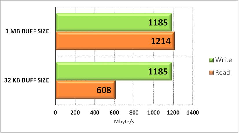
Figure 4‑1 Test Performance of NVMeTCP10G-IP demo
Write performance consistently ranges between 1100 - 1200 MB/sec for various buffer sizes. While the Read performance varies according to the read buffer size, as specified in the NVMeTCP10G-IP documentation. The maximum read performance reaches approximately 1200 MB/sec with a 1 MB read buffer, while the minimum is about 600 MB/sec with a 32 KB read buffer. The performance variability may be influenced by the resource availability on the target system.
Note: The performance presented in Figure 4‑1 represent the optimal results obtained in our test environment and are subject to variation based on system resources and other external factors.
5 Revision History
|
Revision |
Date |
Description |
|
2.00 |
2-May-24 |
- Add MACRxAsync32to64IF and MACTxAsync64to32IF modules for supporting Multirate Ethernet MAC Hard IP for Versal ACAP - Update firmware and function list description |
|
1.01 |
25-Mar-22 |
Update register map |
|
1.00 |
4-Nov-21 |
Initial Release |
Copyright: 2021 Design Gateway Co,Ltd.