2.4 Xilinx Transceiver (PMA for 10GBASE-R)
3.9 Start server for listen connection
1 Introduction
This document describes the details of the QUIC Server 10Gbps IP core (QUIC10GS-IP) reference design. In this reference design, the QUIC10GS-IP is used as a medium to transfer data within a secure connection following the QUIC transport protocol version 1 standard (RFC9000). This process involves handling the TLS 1.3 handshake and dealing with data encryption/decryption and flow control. Users can set network parameters, download and upload payloads to the client by inputting supported command via the serial console. Further details regarding the hardware design and CPU firmware are provided below.
2 Hardware Overview
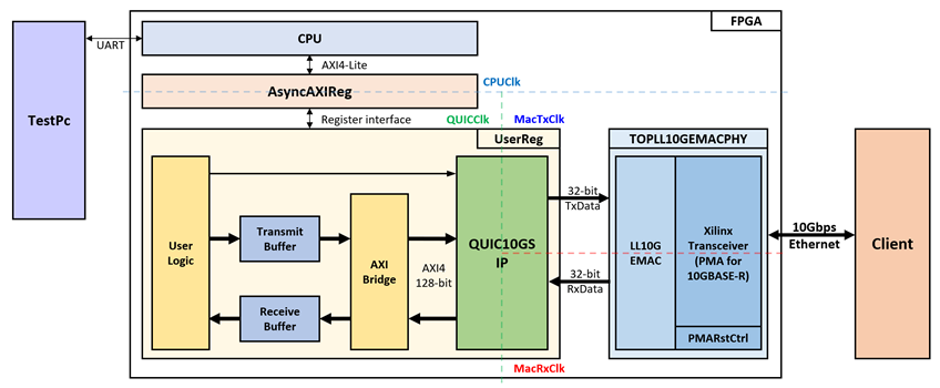
Figure 1 QUIC10GS-IP reference design block diagram
In this test environment, two devices are used to transfer data over a 10G Ethernet connection. The FPGA acts as the QUIC Server, while the target device, which can be either a PC or another FPGA, acts as the QUIC Client. As shown in Figure 1, the QUIC10GS-IP is integrated within UserReg. UserReg connects to the CPU through AsyncAXIReg using a register interface, and the CPU connects to AsyncAXIReg via an AXI4-Lite interface.
The user interface of the QUIC10GS-IP connects to AXIBridge via an AXI4 interface for reading data from the Transmit Buffer and writing data to the Receive Buffer. The user logic is responsible for generating the sending data, verifying the receiving data, and other user control operations for the QUIC10GS-IP.
There are four system clocks in this reference design, i.e., CPUClk, QUICClk, MacTxClk and MacRxClk. CpuClk is used to interface with CPU through AXI4-Lite bus. QUICClk is the clock domain on which the QUIC10GS-IP operates and interfaces with users. MacTxClk is the clock domain which is synchronous to Tx EMAC interface. MacRxClk is the clock domain which is synchronous to Rx EMAC interface.
The details of each module are described as follows.
2.1 AsyncAxiReg
This module is designed to convert the signal interface of AXI4-Lite to be register interface. Also, it enables two clock domains to communicate.
To write register, RegWrEn is asserted to ‘1’ with the valid signal of RegAddr (Register address in 32-bit unit), RegWrData (write data of the register), and RegWrByteEn (the byte enable of this access: bit[0] is write enable for RegWrData[7:0], bit[1] is used for RegWrData[15:8], …, and bit[3] is used for RegWrData[31:24]).
To read register, AsyncAxiReg asserts RegRdReq=’1’ with the valid value of RegAddr (the register address in 32-bit unit). After that, the module waits until RegRdValid is asserted to ‘1’ to get the read data through RegRdData signal at the same clock.
The address of Register interface is shared for both write and read transactions, so user cannot write and read the register at the same time. The timing diagram of the Register interface is shown Figure 2.
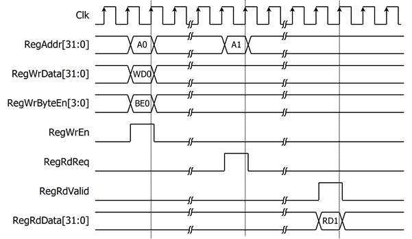
Figure 2 Register interface timing diagram
2.2 UserReg
For register file, UserReg is designed to write/read registers, control and check alert of the QUIC10GS-IP corresponding with write register access or read register request from AsyncAvlReg module. The memory map inside UserReg module is shown in Table 1.
Table 1 Register map Definition of QUIC10GS-IP
|
Address |
Register Name |
Rd/Wr |
Description |
|
Ethernet MAC register |
|||
|
0x0060 |
EMAC_VER_INTREG |
Rd |
[31:0]: LL10GEMAC-IP Version (MacIPVersion). |
|
0x0064 |
EMAC_STS_INTREG |
Rd |
[0]: Linkup status of LL10GEMAC-IP (MacLinkup). |
|
QUIC10GS Control register |
|||
|
0x0100 |
QUIC_RSTB_REG |
Wr/Rd |
[0]: Reset signal active low (rQUICRstBOut). |
|
0x0104 |
QUIC_CONN_REG |
Wr/Rd |
[0]: User’s Connection status. (rQUICConnOn). |
|
0x0108 |
QUIC_BUSY_REG |
Rd |
[3]: Data receive operation busy status (QUICRxTrnsBusy). [2]: Data transmit operation busy status (QUICTxTrnsBusy) [1]: Handshake operation busy status (QUICHandshakeBusy) [0]: Connection operation busy status (QUICConnOnBusy). |
|
0x010C |
QUIC_ALERT_REG |
Rd |
[15:0]: Normal and alert conditions of the QUIC10GS-IP (QUICAlertCode[15:0]). |
|
QUIC User Data |
|||
|
0x0120 |
QUIC_TX_BASE_ADDR_LOW_REG |
Wr |
[31:0]: Lower 32 bits of the base address for the transmit buffer (AppTxBaseAddr[31:0]) |
|
0x0124 |
QUIC_TX_BASE_ADDR_HIGH_REG |
Wr |
[31:0]: Upper 32 bits of the base address for the transmit buffer (AppTxBaseAddr[63:32]) |
|
0x0128 |
QUIC_RX_BASE_ADDR_LOW_REG |
Wr |
[31:0]: Lower 32 bits of the base address for the receive buffer (AppRxBaseAddr[31:0]) |
|
0x012C |
QUIC_RX_BASE_ADDR_HIGH_REG |
Wr |
[31:0]: Upper 32 bits of the base address for the receive buffer (AppRxBaseAddr[63:32]) |
|
0x0140- |
QUIC_TX_USER_PTR_REG |
Rd |
[17:0]: Read pointer of streamID ‘X’ to indicate the first byte position of TxData that IP will process (AppTxRdAddrX[17:0]). |
|
Wr |
[17:0]: Write pointer of streamID ‘X’ to indicate the position after the last TxData written (rAppTxWrAddrX[17:0]). |
||
|
0x0150- |
QUIC_TX_USER_FINAL_REG |
Wr |
[0]: Set the end stream flag of the current Tx write pointer for StreamID ‘X’ (rAppTxWrFinX) |
|
0x0180- |
QUIC_RX_USER_PTR_REG |
Rd |
[17:0]: Write pointer of streamID ‘X’ to indicate the position after the last RxData written (AppRxWrAddrX[17:0]). |
|
Wr |
[17:0]: Read pointer of streamID ‘X’ to indicate the first byte of RxData that user will process (rAppRxRdAddrX[17:0]). |
||
|
0x0190- |
QUIC_RX_USER_FINAL_REG |
Rd |
[0]: Indicating the end of stream has been received for streamID ‘X’ (AppRxWrFinX) |
|
0x01C0 |
QUIC_RX_USER_INFO_READ_REG |
Rd |
[0]: Empty status of QUICRxInfo FIFO, storing QUIC Rx user information (UsrRxInfoFfEmpty). |
|
Wr |
[0]: Set read enable to QUICRxInfo FIFO (UsrRxInfoFfEmpty). |
||
|
0x01C4 |
QUIC_RX_USER_COMMON_REG |
Rd |
[7:0]: QUIC Rx user information type (QUICRxInfoType[7:0]). [15:8]: QUIC Rx user information streamID (QUICRxInfoID[7:0]). |
|
0x01D0- |
QUIC_RX_USER_INFO0_REG |
Rd |
[31:0]: QUIC Rx user information field 0 (QUICRxInfoD0[63:0]) |
|
0x01D8- |
QUIC_RX_USER_INFO1_REG |
Rd |
[31:0]: QUIC Rx user information field 1 (QUICRxInfoD1[63:0]) |
|
0x0200 |
USER_TX_PATT_ADDR_REG |
Rd |
[19:0]: Current write address for writing Tx data pattern to transmit buffer (rTxUserWrPtr[19:0]). |
|
Wr |
[19:0]: Start Address for writing Tx data pattern. |
||
|
0x0204 |
USER_TX_PATT_TYPE_REG |
Wr |
[0]: Data pattern mode (rPattGenMode) “0” for incremental and “1” for decremental 8-bit counter. |
|
0x0208 |
USER_TX_PATT_LEN_REG |
Rd |
[17:0]: Remaining data pattern length (rPattGenLen[17:0]). |
|
Wr |
[17:0]: Length of data pattern (rPattGenLen[17:0]). |
||
|
0x0210 |
USER_RX_VERIFY_ADDR_REG |
Rd |
[19:0]: Read address of the first Rx data that failed verification (rVerifyRxUserRdPtr[19:0]). |
|
Wr |
[19:0]: Start Address for reading Rx data pattern (rRxUserRdPtr[19:0]). |
||
|
0x0214 |
USER_RX_VERIFY_TYPE_REG |
Rd |
[1]: Validity status (wVerifyInvalid) ‘0’ for
indicating that received data is matched with data pattern, ‘1’ for
indicating that received data is NOT matched with data pattern. |
|
Wr |
[0]: Data verification mode (rVerifyMode) “0” for incremental and “1” for decremental 8-bit counter When the data verification mode is set, verification status is reset. |
||
|
0x0218 |
USER_RX_VERIFY_LEN_REG |
Rd |
[17:0]: Remaining data verify length (rVerifyLen[17:0]). |
|
Wr |
[17:0]: Length of verification pattern (rVerifyLen[17:0]). |
||
|
0x0220- |
USER_RX_ACTUAL_DATA |
Rd |
[31:0]: Actual RxData (rVerifyActualData[127:0]). |
|
0x0240- |
USER_RX_EXP_DATA |
Rd |
[31:0]: Expected RxData (rVerifyExpectData[127:0]). |
|
0x0280- |
USER_TX_PATT_DATA_REG |
Rd |
[31:0]: Current data pattern (rPattGenData). |
|
Wr |
[31:0]: Initial data for the data pattern. |
||
|
0x02A0- |
USER_RX_PATT_DATA_REG |
Rd |
[31:0]: Current verification pattern (rVerifyExpData). |
|
Wr |
[31:0]: Initial data for the data verification. |
||
|
0x02E0- |
QUIC_ALPN_DATA_REG0-3 |
Wr |
[31:0]: ALPN string value (QUICALPNStr[127:0]). |
|
0x02F0 |
QUIC_ALPN_LEN_REG |
Wr |
[4:0]: ALPN string length (QUICALPNLen[4:0]). |
|
0x0300- |
QUIC_CTS_REG |
Rd |
[31:0]: Client Traffic Secret (CTS[255:0]) |
|
0x0340- |
QUIC_STS_REG |
Rd |
[31:0]: Server Traffic Secret (STS[255:0]) |
|
0x0380- |
QUIC_RANDOM_REG |
Rd |
[31:0]: Random number in ClientHello message. (Random[255:0]) |
|
0x03C0 |
QUIC_KEY_VALID_REG |
Rd |
[0]: Validity status for key material, key and iv (QUICKeyValid) |
|
0x0400 |
QUIC_UDP_SRCMAC_LOW_REG |
Wr |
[31:0]: Lower 32 bits of source MAC address (rSrcMacAddr[31:0]). |
|
0x0404 |
QUIC_UDP_SRCMAC_HIGH_REG |
Wr |
[15:0]: Upper 16 bits of source MAC address (rSrcMacAddr[47:32]). |
|
0x0408 |
QUIC_UDP_SRCIP_REG |
Wr |
[31:0]: Source IP address (rSrcIPAddr[31:0]) |
|
0x040C |
QUIC_UDP_DSTIP_REG |
Rd |
[31:0]: Destination IP address (wDstIPAddr[31:0]) |
|
0x0410 |
QUIC_UDP_SRCPORT_REG |
Wr |
Wr[15:0]: Source port number (rSrcPort[15:0]). |
|
0x0414 |
QUIC_UDP_DSTPORT_REG |
Rd |
[15:0]: Destination port number (wDstPort[15:0]). |
|
0x041C |
QUIC_UDP_IPNETSET_REG |
Wr |
Wr[0]: Set IP network parameters (rNetworkSet). |
|
0x04FC |
QUIC_VER_REG |
Rd |
[31:0]: QUIC10GS-IP version (QUICIPVersion[31:0]). |
|
0x4000- |
CERTRAM_BASE_ADDR |
Wr/Rd |
[31:0]: Certificate data in CertRam (wRamCertRdData[31:0]). |
|
0x6800 |
RSAKEYRAM_BASE_ADDR |
Wr/Rd |
[31:0]: RSA Key data in RSAKeyRam (wRamRSAKeyRdData[31:0]). |
|
0x200000- |
USER_RXRAM_BASE_ADDR |
Rd |
[31:0]: Rx data read from the receive buffer (UserRxRamRdData). |
|
0x300000- |
USER_TXRAM_BASE_ADDR |
Wr |
[31:0]: Tx data written to the transmit buffer (rUserTxRamWrData). |
Certificate and RSA key information
QUIC10GS-IP is designed to read certificate and RSA key information from the user via the RAM interface. In this reference design, a dual-port RAM is used to store the certificate information. The user writes data to Port A, while Port B is used by QUIC10GS-IP to read the data. As shown in Figure 3, QUICCertRdEn and QUICCertRdAddr[11:0] are used as the read enable and read address for CertRam, respectively. When QUICCertRdEn is asserted to ‘1’, QUICCertRdData[15:0] must be valid in the next clock cycle.
Similarly, QUICRSAKeyRdEn and QUICRSAKeyRdAddr[9:0] are used as the read enable and read address for RSAKeyRam, respectively. When QUICRSAKeyRdEn is asserted to ‘1’, QUICRSAKeyRdData[15:0] must be valid in the next clock cycle, as shown in Figure 4.
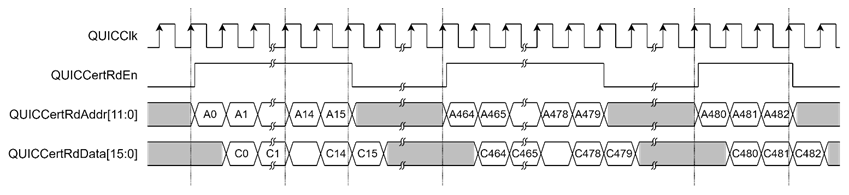
Figure 3 Example timing diagram of reading certificate information
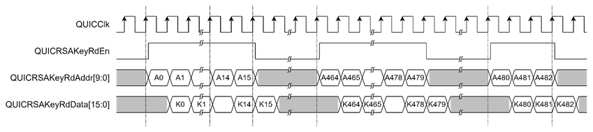
Figure 4 Example timing diagram of reading RSA key information
AXI Bridge
In the reference design, an AXI bridge is used to convert AXI protocol transactions into memory interface operations. The AXI bridge converts AXI write transactions from the QUIC10GS-IP to write receive data into the receive buffer (RxRam) and converts AXI read transactions from the QUIC10GS-IP to read transmit data from the transmit buffer (TxRam).
In the case of sending AXI write requests to the AXI bridge, AxiAwReady will be de-asserted to ‘0’, and AxiwReady will be asserted to ‘1’ in the next clock cycle. The AXI bridge will set Ram0WrAddr[19:0] to AxiAwAddr[19:0], positioning the first address to write data to RxRam. When AxiwReady is ‘1’ and the AXI master is ready to write data, the AXI master will assert AxiwValid to ‘1’. When the AXI bridge receives AxiwValid as ‘1’ from the AXI master, the AXI bridge will forward information in AxiwValid, AxiwStrb[15:0], and AxiwData[127:0] to Ram0WrEn, Ram0WrByteEn[15:0], and Ram0WrData[127:0], respectively. Ram0WrAddr[19:0] will increment by 16 for each AXI master write data word. To ensure data is written correctly, the AXI master must write data for all bytes in a word except the first or last word. When the AXI master transfers data to the last word, it must assert AxiwLast to ‘1’. When AxibReady is ‘1’ and AxibValid is ‘1’, it signifies the completion of the write data operation, and the AXI bridge will set AxiAwReady to ‘1’ in the next clock cycle to accept new write requests.
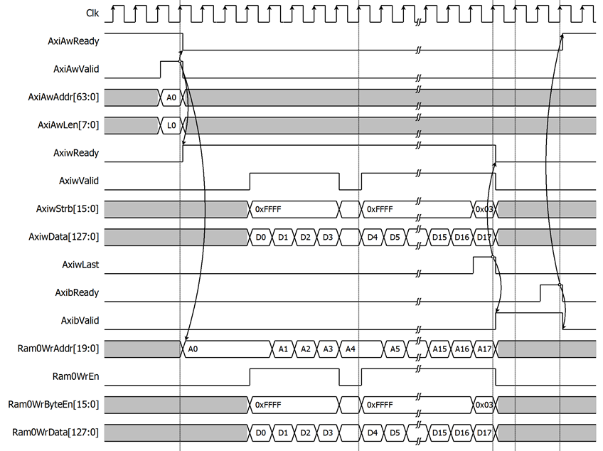
Figure 5 Example timing diagram of writing data to RxRam via AXI bridge
In the case of reading AXI read requests to the AXI bridge, AxiArReady will be de-asserted to ‘0’ in the next clock cycle. The AXI bridge will set Ram1RdAddr[19:0] to AxiArAddr[19:0], positioning the first address to read data from TxRam. The AXI bridge will read data and store it in an internal buffer, and Ram1RdAddr[19:0] will increment by 16 until the read operation is finished. When the AXI bridge is ready to transfer data to the AXI master and the AXI master is ready to receive data, the AXI bridge will assert AxirValid to ‘1’. When the AXI bridge transfers data to the last word, it will assert AxirLast to ‘1’ to specify the last cycle. When the AXI bridge sends AxirLast=‘1’ and the AXI master sends AxirReady=‘1’, it signifies the completion of the read data operation, and the AXI bridge will set AxiArReady to ‘1’ in the next clock cycle to accept new read requests.
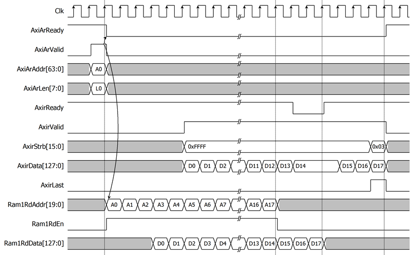
Figure 6 Example timing diagram of reading data to TxRam via AXI bridge
User Data Generator
For example, if the user want to generate a data pattern for transmitting data in streamID0, user can set the start address to 0x1F and set rPattGenLen[17:0] to generate a 451-byte increasing binary pattern. rUserTxRamWrData[127:120] is set to 0x00 and rUserTxRamWrByteEn[15:0] is set to 0x8000 at the first clock cycle to write data only to the highest byte at rUserTxRamWrAddr[19:4]=0x0001. At the second clock cycle, every byte of the data pattern is written. At the last clock cycle, only the last 2 bytes of the data pattern are written: rUserTxRamWrData[15:0] is set to 0xC2C1 and rUserTxRamWrByteEn[15:0] is set to 0x0003, as shown in Figure 7.
The user can check if the data pattern write to TxRam is complete by verifying that rPattGenLen[17:0]=0, which can be read from USER_TX_PATT_LEN_REG. Once the data pattern generation is complete, the user can update the write pointer (rAppTxWrAddr0[17:0]) by writing to QUIC_TX_USER_PTR_REG0, indicating to QUIC10GS-IP that there is available Tx data to transmit. When the user wants to determine that the end of the data in the stream has been reached, they can assert rAppTxWrFin0 to ‘1’ by writing to QUIC_TX_USER_FINAL_REG0.
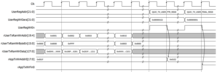
Figure 7 Example timing diagram of user data generation process
User Data Verification
For example, if the user wants to verify a data pattern from received data in streamID0, the user can set the start address to 0x1F and set rVerifyLen[17:0] to verify a 451-byte increasing binary pattern. UserRdIF will read data from RxRam into VerifyRdData[127:0] and compare it with wVerifyExpData[127:0] when wVerifyByteEn is active. At the last clock cycle, only the last 3 bytes of the data pattern are verified, wVerifyByteEn[15:0] is set to 0x0007, and wVerifyExpData[23:0] is set to 0xC2C1C0, as shown in Figure 8.
The user can check if the data pattern verification from RxRam is complete by verifying that rVerifyLen[17:0]=0, which can be read from USER_RX_VERIFY_LEN_REG. Once the data pattern verification is complete, the user can update the read pointer (rAppRxRdAddr0[17:0]) by writing to QUIC_RX_USER_PTR_REG0, indicating to QUIC10GS-IP that the data has been processed. If the other endpoint requests to close streamID0, the QUIC10GS-IP will set AppRxWrFin0 to ‘1’, which can be read from QUIC_RX_USER_FINAL_REG0.
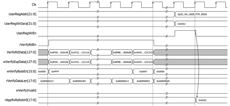
Figure 8 Example timing diagram of user data verification process
2.3 LL10GEMAC
The IP core by Design Gateway implements low-latency EMAC and PCS logic for 10Gb Ethernet (BASE-R) standard. The user interface is 32-bit AXI4-stream bus. Please see more details from LL10GEMAC datasheet on our website.
https://dgway.com/products/IP/Lowlatency-IP/dg_ll10gemacip_data_sheet_xilinx_en/
2.4 Xilinx Transceiver (PMA for 10GBASE-R)
PMA IP core for 10Gb Ethernet (BASE-R) can be generated by using Vivado IP catalog. In FPGA Transceivers Wizard, the user uses the following settings.
· Transceiver configuration preset : GT-10GBASE-R
· Encoding/Decoding : Raw
· Transmitter Buffer : Bypass
· Receiver Buffer : Bypass
· User/Internal data width : 32
The example of Transceiver wizard in Ultrascale model is described in the following link.
https://www.xilinx.com/products/intellectual-property/ultrascale_transceivers_wizard.html
2.5 PMARstCtrl
When the buffer inside Xilinx Transceiver is bypassed, the user logic must control reset signal of Tx and Rx buffer. The module is designed by state machine to run following step.
1) Assert Tx reset of the transceiver to ‘1’ for one cycle.
2) Wait until Tx reset done, output from the transceiver, is asserted to ‘1’.
3) Finish Tx reset sequence and de-assert Tx reset to allow the user logic beginning Tx operation.
4) Assert Rx reset to the transceiver.
5) Wait until Rx reset done is asserted to ‘1’.
6) Finish Rx reset sequence and de-assert Rx reset to allow the user logic beginning Rx operation.
3 CPU Firmware
After system boot-up, CPU initializes its peripherals such as UART and Timer. Then the supported command usage is displayed. The main function runs in an infinite loop to receive line command input from the user. Users can set the network and connection parameters, display key materials and certificate information, download/upload data and test performance using the supported commands. More details of the sequence in each command are described as follows.
3.1 Set FPGA’s IP Address
command> setip ddd.ddd.ddd.ddd
Users can set an IP address for the QUIC10GS-IP by inputing setip followed by the desired IP address in dotted-decimal format. The setip function is called to change the IP address value in netparam variable. This variable will be written to the register mapped to SrcIPAddr to set the FPGA’s IP address. Subsequently, the QUIC10GS-IP is initialized with the current network parameter setting. The default FPGA’s IP address is 192.168.7.42. The setip function is described in Table 2.
Table 2 setip function
|
int setip(char *string, uint32_t *ip_set) |
|
|
Parameter |
string: ip address as string input from user ip_set: array stored IP address |
|
Return value |
0: Valid input, -1: Invalid input |
|
Description |
This function receives IP Address as string input and set value of ip_set array. |
3.2 Set FPGA’s Port Number
command> setport ddddd
Users can set a port number to the QUIC10GS-IP by inputting setport followed by the static port number of the FPGA in decimal format. The setport function is called to change the port number value in netparam variable. This variable will be written to the register mapped to SrcPort to set the FPGA’s port number. Subsequently, the QUIC10GS-IP is initialized with the current network parameter setting. The default FPGA’s port number is 4433. The setport function is described in Table 3.
Table 3 setport function
|
int setport(char *string, uint16_t *port_set) |
|
|
Parameter |
string: port number as string input from user port_set: array stored port number |
|
Return value |
0: Valid input, -1: Invalid input |
|
Description |
This function receives port number as string input and set value of port_set array. |
3.3 Set FPGA’s MAC address
command> setmac hh-hh-hh-hh-hh-hh
Users can set a MAC address to the QUIC10GS-IP by inputing setmac followed by the FPGA’s MAC address in hexadecimal format. The setmac function is called to change the MAC address value in netparam variable. This array will be written to the register mapped to SrcMacAddr to set the FPGA’s MAC address. The default FPGA’s MAC address is 80-01-02-03-04-05. The setmac function is described in Table 4.
Table 4 setmac function
|
int setmac(char *string, uint64_t *mac_set) |
|
|
Parameter |
string: MAC address as string input from user mac_set: array stored mac address |
|
Return value |
0: Valid input, -1: Invalid input |
|
Description |
This function receives MAC Address as string input and set value of mac_set array. |
3.4 Show key materials
command> showkey <1: enable, 0: disable>
*Wireshark, a network packet analyzer tool used for network troubleshooting, analysis, and security purposes.
3.5 Set certificate
Command> setcert
The setcert command allows users to set the server’s certificate. After entering the setcert command, users can send an ASN.1 DER certificate file in binary format (up to 8 kB) via the serial connection. The certificate data is written to the CertRam memory using the fill_mem_with_wrapper function. Details about the fill_mem_with_wrapper is described in Table 5. It is essential for users to set the certificate before starting a server.
Table 5 fill_mem_with_wrapper function
|
int fill_mem_with_wrapper (uint32_t *base_addr, uint32_t mem_size8) |
|
|
Parameter |
base_addr: base address of the memory where the data will be written. mem_size8: Maximum size of the memory (in bytes) that can be filled. |
|
Return value |
0: Valid input, -1: Invalid input |
|
Description |
This function writes the binary data from serial console to memory starting at base address. It ensures that the data does not exceed the allocated memory size (mem_size8). |
3.6 Set RSA key information
Command> setrsakey
The setrsakey command allows users to set the RSA private key information. After entering the setrsakey command, users can send an ASN.1 DER RSA private key file in binary format (up to 2 kB) via the serial connection. The RSA key data is written to the RSAKeyRam memory using the fill_mem_with_wrapper function. It is essential for users to set the RSA key before starting a server.
3.7 Print certificate
command> printcert
The printcert command is used to display the server’s certificate. The certificate is shown in a structured hexadecimal representation. The certificate data is read from CertRam and displayed using the showder function. Details about the showder is described in Table 6. This command is useful for verifying that the certificate is correctly set and valid before starting the server.
Table 6 showder function
|
void showder (uint32_t *base_addr, uint32_t max_size) |
|
|
Parameter |
base_addr: Pointer to the start of the binary data (certificate or RSA key in DER format). max_size: Maximum size of the data to be displayed, in bytes. |
|
Return value |
None. |
|
Description |
The function displays binary data (e.g., a certificate or RSA key) in ASN.1 DER format in a hexdump-style format. |
3.8 Print RSA key information
command> printrsakey
The printrsakey command is used to display the server’s rsa key. The rsa key is shown in a structured hexadecimal representation. The rsa key data is read from RSAKeyRam and displayed using the showder function. This command is useful for verifying that the rsa key is correctly set and valid before starting the server.
3.9 Start server for listen connection
command> Listen
This command is used for performance testing using the unique application protocol with MsQuic. The ListenPREF function is called to configure registers, start data generation, verify data patterns, and monitor status. The sequence of the ListenPREF function is as follows.
1) Set network parameters by configuring the FPGA IP address, port number, and MAC address to establish a connection with the MsQuic client.
2) Wait for new connection. The server listens for incoming connections from the MsQuic client. When a client connects, a QUIC handshake is performed to establish a secure session.
3) Extract uploadSize from the MsQuic client request. Monitor verification status and calculate the download length from the total data received from the client.
4) If uploadSize is greater than zero, set USER_TX_PATT_LEN_REG to generate pattern data in TxRam. Move rAppTxWrAddr0[17:0] by writing to QUIC_TX_USER_PTR_REG until TxRam is fully populated. Monitor the upload status.
5) Compute and display transfer speed on the serial console until data reception is complete. If received data length is less than 4 kB, the data will be displayed on the console.
6) Loop to step 2 to wait for new connection.
Table 7 ListenPREF function
|
int ListenPREF() |
|
|
Return value |
0: Operation completes successfully. -1: Connection aborted by the user. |
|
Description |
This function listens for incoming QUIC connections, performs a handshake, and facilitates data transfer (upload and download). It calculates transfer speed, verifies data integrity, and handles errors. The function operates in a loop until the connection is terminated. |
4 Revision History
|
Revision |
Date (D-M-Y) |
Description |
|
1.00 |
11-Mar-25 |
Initial version release |