SATA AHCI IP Core Data Sheet

Core Facts |
|
|
Provided with Core |
|
|
Documentation |
User Guide, Design Guide |
|
Design File Formats |
Encrypted hdl File |
|
Instantiation Templates |
VHDL |
|
Reference Designs & Application Notes |
QuartusII Project, See Reference Design Manual |
|
Additional Items |
Demo on CycloneV SX SoC development kit ArriaV ST SoC development kit Arria10 SoC development kit |
|
Support |
|
|
Support Provided by Design Gateway Co., Ltd. |
|
Design Gateway Co.,Ltd
54 BB Building 14th Fl., Room No.1402 Sukhumvit 21 Rd. (Asoke), Klongtoey-Nua, Wattana, Bangkok 10110
Phone: (+66) 02-261-2277
Fax: (+66) 02-261-2290
E-mail: sales@design-gateway.com
URL: www.design-gateway.com
Features
· Compliant with the Serial ATA Advanced Host Controller Interface (AHCI) 1.3.1, but memory to store Command List Table, Received FIS Table, and Command Table uses block memory inside IP instead of main memory
· Support up to 120 PRD entries per command
· Register controlled by RAM interface
· 64-bit AXI4 bus for data interface
· Support up to 4 GB main memory for DMA engine
· Support Native Command Queuing (NCQ)
· AHCI IP Reference design available on CycloneV SX SoC board (with HSMC2SATA adapter board, provided by Design Gateway)/ArriaV ST/Arria10 SoC board (with FMCRAID adapter board, provided by Design Gateway)
· Multiple ports for RAID application can be designed by using multiple SATA AHCI IP
· Support SATA-III (ArriaV ST/Arria10 SoC) or SATA-II speed (CycloneV SX SoC)
Table 1: Example Implementation Statistics
|
Family |
Example Device |
Fmax (MHz) |
Logic utilization (ALMs) |
Registers1 |
Block Memory bit |
Design Tools |
|
CycloneV SX |
5CSXFC6D6F31C6 |
100 |
636 |
1096 |
666,112 |
Quartus 15.1 |
|
ArriaV ST |
5ASTFD5K3F40I3 |
150 |
629 |
1084 |
666,112 |
Quartus 15.1 |
|
Arria10 SX |
10AS066N3F40E2SGE2 |
150 |
615 |
1061 |
666,112 |
Quartus 16.0 |
Notes:
1) Actual logic resource dependent on percentage of unrelated logic
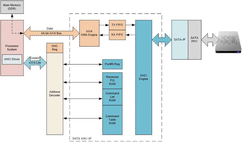
Figure 1 SATA AHCI IP Block Diagram
Applications
SATA AHCI IP core operating with SATA IP Core is suitable for the system which has the processor running on OS and needs to have SATA device to be the system storage. By using AHCI driver to access AHCI IP, the system can access SATA device with full features and high speed performance. ARM on CycloneV/ArriaV/Arria10 SoC platform can be used to be the processor for AHCI IP, so the IP can be applied for embedded storage system, RAID application, high-speed and large capacity data acquisition system
General Description
Register in AHCI standard can be split into two groups, i.e. Host control and Port control. Host control is global signal of every channel and shows channel available. The host control register is provided in HDL format in the reference design for user modifying to support multichannel. While Port control register which is the control/status of each channel is built-in SATA AHCI IP.
For simple design, memory of received FIS, command List, and command Table are designed by using Memory block instead of main memory (DDR). By using command list, the host can use NCQ command with 32 queue depth to access SATA device which can increase higher performance for nonsequential access. By using command table, the host does not need to arrange the data of one command in contiguous area, but can arrange data in many segments. The IP can support up to 120 data segments per command.
The basic sequence for the host to write/read data with SATA device is follows. The host monitors Port#0 Reg to confirm that the IP and device are ready to receive new command. After that, Command FIS and memory address for data allocation will be written to Command List and Table RAM. Next, AHCI engine dumps Command FIS from the RAM to SATA-IP, and then transfer data between main memory and SATA-IP by DMA engine. Data direction depends on the command that is write or read command. Status packet returned from SATA device will be stored to Received FIS RAM.
IP interface for the host processor can be split into two signal groups, i.e. 64-bit AXI4-Master interface for DMA data transfer, and 32-bit register interface for register access. Data port can direct connect to AXI4 bus of the host system while register interface must pass address decoder which is provided in HDL code in the reference design for connecting to AXI4-Lite bus in slave side. Also, SATA AHCI IP has the interface to connect with SATA-IP directly
AHCI driver for LinuxOS is also provided in AHCI IP reference design. The driver is modified from standard driver to move memory of received FIS, command list, and command table from main memory to hardware register area. User can develop the new application to access SATA device through this driver. The reference design can be evaluated before purchasing
Functional Description
As shown in Figure 1, SATA AHCI IP consists of three blocks, i.e. AXI4 DMA engine for data interface, Register and RAM for control/status signals, and AHCI Engine for main controller.
AXI4 DMA Engine
AXI4 DMA Engine is designed for data burst transfer between main memory in Processor system and TX/RX FIFO inside the IP. Data on SATA device is always aligned in sector unit (512-byte), so AXI4 DMA engine is designed to set burst size to be 512-byte or 2048-byte for high performance. TX/RX FIFO is applied to convert data bus size between 64-bit (AXI4 bus size) and 32-bit (SATA-IP bus size). Main memory address and total transfer size of each transaction in DMA engine are decoded from Command Table RAM by AHCI Engine.
Register and RAM
Following AHCI standard, two register areas are defined, i.e. GHC Reg and Port#0 Reg. Address decoder and GHC register are provided in HDL code, so user can modify to remap non-standard register area such as Received FIS RAM, Command List RAM, and Command Table RAM to other address. Based on the reference design, five register areas are mapped as shown in Table 2: Register map. To support multiple channels, address decoder must be modified to decode address for Port#0 Reg, and other three RAMs for additional SATA channel. Also, the value in GHC register must be modified to show the host process that additional channel is connected in the system.
The details of Received FIS RAM, Command List RAM, and Command Table RAM are shown in Figure 3 - Figure 5. Comparing to AHCI standard, Command Table Base Address (CTBA) in Command List RAM is not available because the table has been moved from main memory to be RAM. Otherwise, the IP can support 32-bit address main memory or 4 GB size, so upper 32-bit address of Data Base (DBAU) is not available.
Table 2: Register map
|
Address[16:0] |
Description |
|
0x00000 -0x0002B |
Generic Host Control. Register map in this zone is designed following “topic 3.1 Generic Host Conrol” in “Serial ATA AHCI 1.3.1 Specification”. |
|
0x0002C – 0x000FF |
Reserved |
|
0x00100 – 0x0017F |
Port 0 port control registers. Register map in this zone is designed following “topic 3.3 Port Registers” in “Serial ATA AHCI 1.3.1 Specification”. |
|
0x00180 – 0x010FF |
Port 1 – port 31 control registers. |
|
0x01100 – 0x07FFF |
Reserved |
|
0x08000 – 0x080FF |
Received FIS. Address map in this zone is designed following “topic 4.2.1 Received FIS Structure” in “Serial ATA AHCI 1.3.1 Specification”. |
|
0x08100 – 0x08FFF |
Reserved |
|
0x09000 – 0x093FF |
Command List Structure. Address map in this zone is designed following “topic 4.2.2 Command List Structure” in “Serial ATA AHCI 1.3.1 Specification”. |
|
0x09400 – 0x0FFFF |
Reserved |
|
0x10000 – 0x1FFFF |
Command Table. Address map in this zone is designed following “topic 4.2.3 Command Table” in “Serial ATA AHCI 1.3.1 Specification”. Up to 120 entries are supported. |
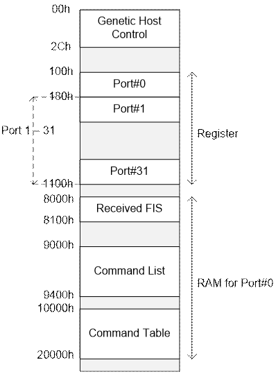
Figure 2 Register memory map
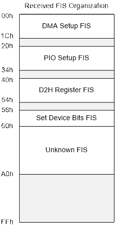
Figure 3 Memory map of Received FIS RAM
Figure 4 Memory map of Command List RAM
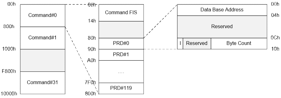
Figure 5 Memory map of Command Table RAM
AHCI Engine
This module is main controller which receives start signal from Processor through Port#0 Reg, and then send/receive the packet with SATA-IP following the sequence of each SATA command. Based on command queue feature, the host can send up to 32 commands to SATA device, and the device can select which command will operate firstly. To support multiple commands, AHCI Engine is designed to send command from Command Table RAM to SATA-IP when command is available in the slot. At the same time, the engine needs to be ready to store the returned FIS from SATA-IP such as DMA Setup FIS to Received FIS RAM. Sometimes, data collision between Command FIS and DMA Setup FIS will be found. Following SATA standard, the device has higher priority than the host, so IP will automatically retry to send Command FIS after data collision situation. Otherwise, as shown in Figure 5 AHCI Engine decodes main memory address and size of each PRD from the active command slot, selected by DMA Setup FIS from SATA device. Then, the engine sends the information to AXI4 DMA Engine to start data transferring between main memory and SATA-IP. If data is splitted into many segments, address and length of next PRD will be loaded to AXI4 DMA Engine at the end of current PRD. Error flag for asserting interrupt will be set if total PRD count or the length is not enough for that Command. If ‘I’ flag in PRD is set, interrupt signal will be asserted when end of PRD transfer.
Processor System
AHCI IP reference design implements on CycloneV/ArriaV/Arria10 SoC platform, so processor is ARM CPU and some peripherals in Processor system such as UART, timer, and main memory controller are enabled. The sequence of AHCI operation is controlled by software on CPU.
SATA-IP
SATA-IP is provided by DesignGateway. More details of SATA-IP can be checked from our website.
http://www.dgway.com/SATA-IP_A_E.html
Core I/O Signals
Descriptions of all signal I/O are provided in Table 3.
Table 3: Core I/O Signals
|
Signal |
Dir |
Description |
|
System signal |
||
|
Reset |
In |
Reset signal. |
|
Clk |
In |
Clock input signal. At least 150 MHz for SATA-III speed, 75 MHz for SATA-II speed. |
|
AHCIBusy |
Out |
Busy status of AHCI IP. Assert when AHCI is not in idle state. |
|
AHCIInt |
Out |
Interrupt signal. Assert when any bit in port interrupt status register (P0IS register) is asserted and the interrupt enable of that bit is allowed (P0IE.bit=’1’). |
|
Register and RAM Interface |
||
|
SlAddr[6:2] |
In |
Port#0 register address for write/read access in 32-bit unit. So, bit[1:0] of byte address is not connected to IP. |
|
SlWrData[31:0] |
In |
Write data bus to Port#0 register. |
|
SlWrEn[3:0] |
In |
Write enable of Port#0 register, referred to each byte in 32-bit SlWrData. Bit0-SlWrData[7:0], … , and bit3-SlWrData[31:24]. Asserted at the same clock with valid value of SlAddr and SlWrData. |
|
SlRdData[31:0] |
Out |
Read data bus from Port#0 register. Valid after SlAddr about one clock. |
|
RxFisMemAddr[7:2] |
In |
Timing diagram of RxFis RAM is same as Port#0 register access, but address range is 256 byte by using bit7 to 2. More details of timing diagram is shown in Figure 7. |
|
RxFisMemWrData[31:0] |
In |
|
|
RxFisMemWrEn[3:0] |
In |
|
|
RxFisMemRdData[31:0] |
Out |
|
|
CLstMemAddr[9:2] |
In |
Timing diagram of Command List RAM is same as Port#0 register access. Address range is 1024 byte. |
|
CLstMemWrData[31:0] |
In |
|
|
CLstMemWrEn[3:0] |
In |
|
|
CLstMemRdData[31:0] |
Out |
|
|
CTblMemAddr[15:2] |
In |
Timing diagram of Command List RAM is same as Port#0 register access. Address range is 65536 byte. |
|
CTblMemWrData[31:0] |
In |
|
|
CTblMemWrEn[3:0] |
In |
|
|
CTblMemRdData[31:0] |
Out |
|
|
Signal |
Dir |
Description |
|
AXI4 Interface (Master side) |
||
|
M_AXI_araddr[31:0] |
Out |
Read address bus. The starting address for the requested read transaction. |
|
M_AXI_arlen[7:0] |
Out |
Read address burst length. Specified the requested read transaction length in data beats – 1. |
|
M_AXI_arready |
In |
Read address ready. Indicates target is ready to accept the read address. |
|
M_AXI_arvalid |
Out |
Read address valid. Indicates that M_AXI_araddr is valid. |
|
M_AXI_awaddr[31:0] |
Out |
Write address bus. The starting address for the requested write transaction. |
|
M_AXI_awlen[7:0] |
Out |
Write address burst length. Specified the requested write transaction length in data beats – 1. |
|
M_AXI_awready |
In |
Write address ready. Indicates target is ready to accept the write address. |
|
M_AXI_awvalid |
Out |
Write address valid. Indicates that M_AXI_awaddr is valid. |
|
M_AXI_bvalid |
In |
Write response valid. Indicates response M_AXI_bresp is valid. |
|
M_AXI_rdata[63:0] |
In |
Read data bus. Read data bus for the requested read transaction. |
|
M_AXI_rlast |
In |
Read data last. Indicates the last data beat of a burst transaction. |
|
M_AXI_rready |
Out |
Read data ready. Indicates that IP is ready to accept read data. |
|
M_AXI_rvalid |
In |
Read data valid. Indicates M_AXI_rdata is valid. |
|
M_AXI_wdata[63:0] |
Out |
Write data bus. |
|
M_AXI_wlast |
Out |
Write data last. Indicates the last data beat of a burst transaction. |
|
M_AXI_wready |
In |
Write data ready. Indicates that target is ready to accept write data. |
|
M_AXI_wvalid |
Out |
Write data valid. Indicates that M_AXI_wdata is valid. |
|
SATA-IP Interface |
||
|
SataRstB |
Out |
Reset output to SATA-IP. Active low. |
|
trn_clk |
Out |
Clock signal to SATA-IP. Source from Clk input signal directly. |
|
trn_td[31:0] |
Out |
Transmit data bus to SATA-IP. |
|
trn_teof_n |
Out |
Transmit end-of-frame. Indicates end of SATA FIS packet. Active low. |
|
trn_tsrc_rdy_n |
Out |
Transmit source ready. Indicates that trn_td is valid. Active low. |
|
trn_tsrc_dsc_n |
Out |
Transmit abort from the IP. Active low. |
|
trn_tdst_rdy_n |
In |
Transmit ready. Indicates that the target is ready to accept data. Active low. |
|
trn_tdst_dsc_n |
In |
Transmit abort from the target. Active low. |
|
trn_rd[31:0] |
In |
Receive data bus from SATA-IP. |
|
trn_rsof_n |
In |
Receive start-of-frame. Indicates start of SATA FIS packet. Active low. |
|
trn_reof_n |
In |
Receive end-of-frame. Indicates end of SATA FIS packet. Active low. |
|
trn_rsrc_rdy_n |
In |
Receive source ready. Indicates that trn_rd is valid. Active low. |
|
trn_rsrc_dsc_n |
In |
Receive disconnect from SATA-IP. Active low. |
|
trn_rdst_rdy_n |
Out |
Receive ready. Indicate that the IP is ready to accept data. Active low. |
|
trn_rdst_dsc_n |
Out |
Receive disconnect from the IP. Active low. |
|
SATA PHY Interface |
||
|
GEN3 |
In |
SATA speed information. ‘0’: SATA2 (3.0 Gbps), ‘1’: SATA3 (6.0 Gbps) |
|
LINKUP |
In |
SATA-PHY link up. Indicates that SATA device is ready. |
|
COMINIT |
In |
COMINIT detect from PHY. Indicates that new device is detected. |
|
COMWAKE |
In |
COMWAKE detect from PHY. Indicates that OOB initialization phase complete. |
Timing Diagram
To acess Port#0 register and memory inside the IP, timing diagram of these interfaces are shown in Figure 6 and Figure 7.
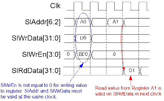
Figure 6 Timing diagram to access Port#0 register
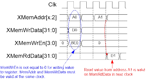
Figure 7 Timing diagram to access RxFis, Command List, and Command Table RAM
For M_AXI port, timing diagram is followed ARM AXI4 specification, which can download from www.amba.com. Also, the details of signal to interface with SATA-IP is described in SATA-IP datasheet.
Verification Methods
The SATA AHCI IP Core functionality was verified by simulation and also proved on real board design by using CycloneV/ArriaV/Arria10 SoC board.
Recommended Design Experience
Experience design engineers with a knowledge of QSys in Quartus tool should easily integrate this IP into their design.
Ordering Information
This product is available directly from Design Gateway Co., Ltd. Please contact Design Gatway Co., Ltd. for pricing and additional information about this product using the contact information on the front page of this datasheet.
Revision History
|
Revision |
Date |
Description |
|
1.0 |
Jan-8-2016 |
New release |
|
1.1 |
Mar-1-2016 |
Support ArriaV ST SoC development board |
|
1.2 |
Jul-27-2016 |
Support Arria10 SoC development board |