SATA HCTL IP Core Data Sheet

Core Facts |
|
|
Provided with Core |
|
|
Documentation |
User Guide, Design Guide |
|
Design File Formats |
Encrypted File |
|
Instantiation Templates |
VHDL |
|
Reference Designs & Application Notes |
QuartusII Project, See Reference Design Manual |
|
Additional Items |
Demo on ArriaV /Arria10 SoC /Arria10 GX Development Kit |
|
Support |
|
|
Support Provided by Design Gateway Co., Ltd. |
|
Design Gateway Co.,Ltd
E-mail: ip-sales@design-gateway.com
URL: design-gateway.com
Features
· Simple user interface by dgIF typeS
· Direct connecting to DG SATA-IP
· Small logic resource without Block Memory utilization
· Operating without CPU and external memory (DDR)
· Support four ATA commands for application layer, i.e., IDENTIFY DEVICE, SECURITY ERASE UNIT, WRITE DMA (EXT), and READ DMA (EXT)
· Reference design with DG SATA-IP by using AB12-HSMCRAID or AB09-FMCRAID adapter board from Design Gateway
Table 1: Example Implementation Statistics
|
Family |
Example Device |
Fmax (MHz) |
Logic utilization (ALMs) |
Registers1 |
Pin |
Block Memory bit |
Design Tools |
|
ArriaV GX |
5AGXFB3H4F35C4 |
277 |
365 |
616 |
- |
- |
QuartusII 15.1 |
|
StratixV GX |
5SGXEA7K2F40C2 |
357 |
370 |
589 |
- |
- |
QuartusII 14.0 |
|
Arria10 SX |
10AS066N3F40E2SG |
384 |
385 |
613 |
- |
- |
QuartusII 16.0 |
Notes:
1) Actual logic resource dependent on percentage of unrelated logic
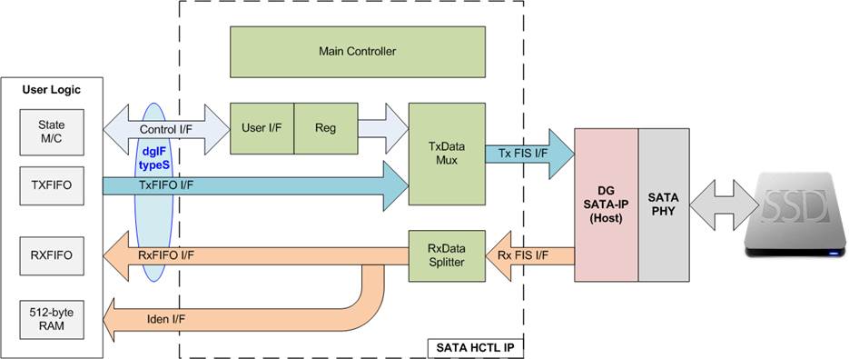
Figure 1: SATA HCTL IP Block Diagram
Applications
SATA HCTL IP Core operating with DG SATA-IP and SATA PHY is ideal to access SATA device without using both CPU and external memory. The resource utilization of the IP is less, but it can achieve very high performance. Using multiple IPs for RAID0 can increase total performance of storage system. So, it is recommended to use the IP in very high-speed data recording system or big-data storage.
General Description
The reference design to test write/read data with SATA-III device on Intel FPGA development board is available to download for evaluation before purchasing.
Functional Description
SATA HCTL IP Core is designed to create/decode SATA FIS interface with DG SATA-IP. The IP is split into two parts, i.e., Data processor and Command processor. Data processor handles the Data FIS packet for transferring by using Data interface of dgIF typeS. While the Command processor handles the non-Data FIS packet which is related to Command interface signal of dgIF typeS. More details of each part are described as follows.
Command Processor
After system power-on, HCTL IP waits until Signature FIS is returned from SATA device and then the initialization is completed. After that, the IP is ready to receive new command from user. When user sends Write/Read command request to HCTL IP, the IP creates Command FIS from user parameters and then forwards it to SATA IP. If total transfer size is more than maximum data size per command (32 MB), the IP automatically creates multiple commands to SATA IP until all data is completely transferred.
· Main Controller
The sequence of transmitted FIS and received FIS while executing each ATA command is controlled by the Main controller. The FIS type of each transmitted packet to SATA IP is defined by this module. Also, the FIS type of the received packet from SATA IP is decoded and checked by this module. The error is asserted by the Main controller when wrong FIS packet sequence is found.
· User I/F and Reg
Command, Address, and transfer size which are inputs from Control I/F are latched to the internal registers when the command is requested. These parameters are applied to build the Command FIS. The status signal that is extracted by received FIS is latched and returned to the user for monitoring.
Data Processor
To create Data FIS for write command, data from TxFIFO is appended by the header to build SATA FIS packet. If transfer data size is more than one FIS packet size, data stream from TxFIFO is split to multiple data blocks for sending to SATA IP in FIS format. For Read command, the header in Data FIS packet is removed and the raw data is extracted and forwarded to RxFIFO interface. While Data output from Identify device command is transferred to Iden I/F, not RxFIFO I/F.
· TxData Mux
Data Multiplexer selects data source and the parameters of each SATA FIS packet, controlled by the Main Controller. The transmitted packet to SATA IP is either Command FIS or Data FIS. The Command FIS sends the parameters from User I/F and Reg while the Data FIS sends data stream from TXFIFO.
· RxData Splitter
Received FIS returned from SATA IP is decoded to check FIS type. If Data FIS is received while operating Read command, the data stream is extracted and stored to RxFIFO I/F. If Data FIS is received while operating Identify device command, the data stream is forwarded to Iden I/F instead. If the received FIS is not Data FIS, the Main controller decodes and determines the operation status to be normal or error.
User Logic
As shown in Figure 1, this block can be designed by using simple logic which consists of State machine and two FIFOs. State machine is designed to create the parameters and check the status of Control I/F. Two FIFOs are connected with Data I/F of SATA HCTL IP for Write/Read command. While 512-byte RAM is applied to store the data from Identify device command.
DG SATA IP
DG SATA IP implements Transport layer and link layer of SATA protocol. It supports for both Host mode and Device mode. To connect with SATA HCTL IP, SATA IP is set to run in Host mode. More details of DG SATA IP are described in the datasheet as following link.
https://dgway.com/products/IP/SATA-IP/Altera/dg_sata_ip_datasheet_altera5_en.pdf
SATA PHY
SATA PHY implements Physical layer of SATA protocol. It consists of the logic for controlling the initialization process of SATA signal in Physical layer. Also, FPGA transceiver is integrated to convert parallel data to be Serial data interface. The characteristic and the parameter of FPGA transceiver for operating SATA protocol of each FPGA model is different.
Core I/O Signals
Descriptions of all I/O signals are provided in Table 2.
Table 2: Core I/O Signals
|
Signal |
Dir |
Description |
|
User Interface |
||
|
RstB |
In |
Synchronous reset signal. Active low. De-assert to 1b after Clk signal input is stable |
|
Clk |
In |
Clock for running HCTL IP. It must be the same signal as trn_clk of SATA IP. (At least 150 MHz for SATA3 operation or at least 75 MHz for SATA2 operation) |
|
dgIF typeS |
||
|
UserCmd[1:0] |
In |
User Command. 00b: Identify device command, 01b: Security erase unit command, 10b: Write SATA device, 11b: Read SATA device. Note: 1) The operation time of Security erase unit command depends on SATA device characteristic. The operation may take long time to complete. So, timeout counter in the IP is disabled while operating Security erase unit command. 2) Security erase unit command is not mandatory command, so user should confirm that the SATA device supports this command before using it. |
|
UserAddr[47:0] |
In |
Start address of SATA device to write/read in sector unit (512 byte). |
|
UserLen[47:0] |
In |
Total transfer size in the request in 512-byte unit. Valid from 1 to (LBASize-UserAddr). |
|
UserReq |
In |
Request the new command. Set to 1b for sending the new command when the IP is Idle (UserBusy=0b). It is asserted along with the valid UserCmd/UserAddr/UserLen signals. |
|
UserBusy |
Out |
IP Busy status. Asserted to 1b when the IP is not ready to receive new command. |
|
LBASize[47:0] |
Out |
Total SATA device capacity in sector unit (512 byte). Default value is 0. This value will be updated after user sends Identify device command. |
|
UserError |
Out |
Error flag. Asserted to 1b when UserErrorType is not equal to 0. The flag can be cleared only by asserting RstB signal. |
|
UserErrorType[31:0] |
Out |
Error status. Details of the error flag. [0] – Error from SATA-IP such as CRC error, wrong primitive sequence. [1] – Error from Data FIS header [2] – Error from returned Status FIS [3] – Error from DMA active FIS. Write operation cannot complete. [4] – Error from PIO Setup FIS. Failure during SATA device identification process. [5] – Timeout error. No FIS returned from SATA device in time. [31:6] - Reserved |
|
UserFifoWrCnt[15:0] |
In |
Write data counter of received FIFO. Used to check full status. If total FIFO size is less than 16-bit, please fill 1b to upper bit. UserFifoWrEn can be asserted to 1b when UserFifoWrCnt[15:3] is not equal to all 1. |
|
UserFifoWrEn |
Out |
Write data valid of received FIFO. Asserted to 1b to write the new data. |
|
UserFifoWrData[31:0] |
Out |
Write data bus of received FIFO. Valid when UserFifoWrEn=1b. |
|
UserFifoRdCnt[15:0] |
In |
This signal is unused for this IP. |
|
UserFifoEmpty |
In |
FIFO empty flag of transmit FIFO to check data available status. Set to 0b when the new UserFifoRdData is ready for reading. |
|
UserFifoRdEn |
Out |
Read valid of transmit FIFO. Asserted to 1b to read the new data. |
|
UserFifoRdData[31:0] |
In |
Read data returned from transmit FIFO. Valid in the next clock after UserFifoRdEn is asserted to 1b. |
|
Signal |
Dir |
Description |
|
Other Interface |
||
|
TestPin[31:0] |
Out |
Reserved to be IP test point. |
|
TimeOutSet[31:0] |
Out |
Timeout value to wait until FIS is returned from SATA device. Time unit is equal to time unit of Clk signal. |
|
IdenWrEn |
Out |
Asserted to 1b when IdenWrAddr and IdenWrData are valid. It is asserted while operating Identify Device command. |
|
IdenWrAddr[6:0] |
Out |
Index of IdenWrData in 32-bit unit. Valid when IdenWrEn=1b. |
|
IdenWrData[31:0] |
Out |
512-byte data from Identify device command. Valid when IdenWrEn=1b. |
|
SATA-IP Interface (Host) |
||
|
trn_rd[31:0] |
In |
Receive data bus from SATA IP. |
|
trn_rsof_n |
In |
Receive start-of-frame. Indicates start of SATA FIS packet. Active low. |
|
trn_reof_n |
In |
Receive end-of-frame. Indicates end of SATA FIS packet. Active low. |
|
trn_rsrc_rdy_n |
In |
Receive source ready. Indicates that trn_rd is valid. Active low. |
|
trn_rsrc_dsc_n |
In |
Receive disconnect from SATA IP. Active low. |
|
trn_rdst_rdy_n |
Out |
Receive ready. Indicate that the IP is ready to accept data. Active low. |
|
trn_rdst_dsc_n |
Out |
Receive disconnect from the IP. Active low. This value is always set to 1b. |
|
trn_td[31:0] |
Out |
Transmit data bus to SATA IP. |
|
trn_teof_n |
Out |
Transmit end-of-frame. Indicates end of SATA FIS packet. Active low. |
|
trn_tsrc_rdy_n |
Out |
Transmit source ready. Indicates that trn_td is valid. Active low. |
|
trn_tsrc_dsc_n |
Out |
Transmit abort from the IP. Active low. This value is always set to 1b. |
|
trn_tdst_rdy_n |
In |
Transmit ready. Indicates that SATA IP is ready to accept data. Active low. |
|
trn_tdst_dsc_n |
In |
Transmit abort from SATA IP. Active low. |
Timing Diagram
Initialization
The sequence of the initialization process is described as follows.

Figure 2: RstB and UserBusy when operating IP initialization
1) RstB is de-asserted to 0b by the user after Clk is stable. UserBusy is asserted to 1b.
2) HCTL-IP waits until Signature FIS returned from SATA device. After that, UserBusy is de-asserted to 0b.
After the initialization process is done, HCTL-IP is ready to receive the command from user.
dgIF typeS
dgIF typeS signal consists of two interfaces, i.e., Command interface and Data interface. Figure 3 shows timing diagram of Command interface of dgIF typeS.

Figure 3: User Command Interface of dgIF typeS Timing diagram
1) Before sending new command to the IP, UserBusy must be de-asserted to 0b to confirm that IP is Idle.
2) UserCmd, UserAddr, and UserLen must be valid while asserting UserReq to 1b for sending the new command.
3) After that, UserBusy changes from 0b to 1b when the IP starts the operation.
4) UserReq is de-asserted to 0b and then the next command can be prepared.
Note: UserAddr and UserLen value are ignored in Identify device command and Security erase command.
For Data interface, Transmit FIFO is read to operate Write command while Received FIFO is written to operate Read command. Timing diagram of Data interface are shown in Figure 4 and Figure 5.
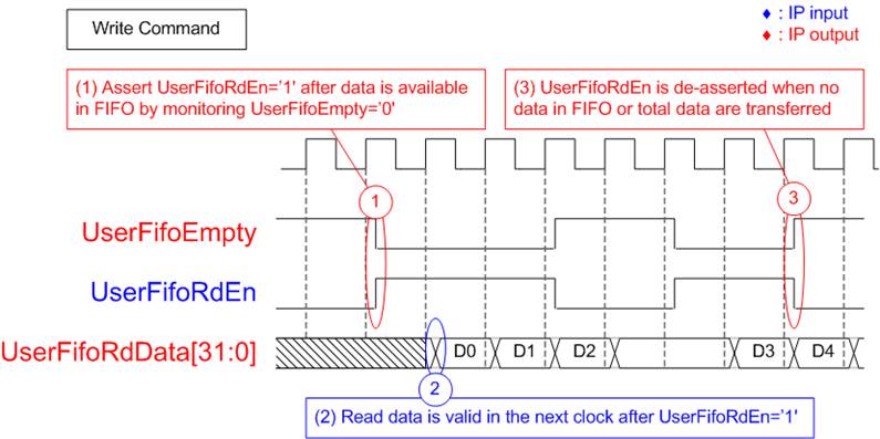
Figure 4: Transmit FIFO Interface for Write command
1) When operating Write command, UserFifoEmpty is monitored to check the available data status. When Transmit FIFO has data (UserFifoEmpty=0b), UserFifoRdEn can be asserted to 1b.
2) The read data from Transmit FIFO (UserFifoRdData) is valid in the next clock after asserting UserFifoRdEn.
3) When there is no remaining data (UserFifoEmpty=1b), UserFifoRdEn must be de-asserted to 0b to pause reading data immediately.
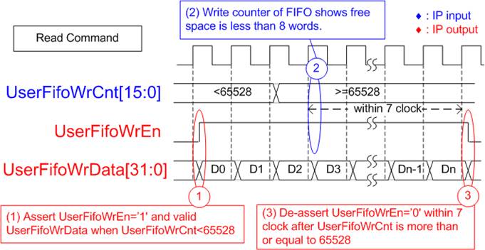
Figure 5: Received FIFO Interface for Read command
1) When operating Read command, UserFifoWrCnt is read to check the free space of FIFO. If UserFifoWrCnt is less than 65528 or the free space is more than 7, UserFifoWrEn can be asserted to 1b along with the valid UserFifoWrData.
2) When UserFifoWrCnt is more than or equal to 65528 which indicates the FIFO is almost full, the IP will pause data transmission.
3) UserFifoWrEn is de-asserted to 0b to pause data transmission within 7 clock cycles after UserFifoWrCnt is more than or equal to 65528.
Identify Device
It is recommended to send Identify device to the IP for the first command after finishing the initialization process. This command is applied to update LBASize signal to show total device capacity. LBASize is applied by the user Logic to check the valid range of the input for Write and Read commands that the sum of address and length is not more than LBASize. The 512-byte data is returned from Identify device command via Iden I/F. The Identify device data shows SATA device information such as model number and supported feature.
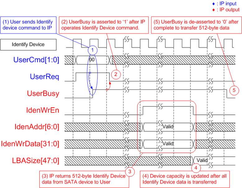
Figure 6: LBASize is updated after Identify Device command
Security Erase Unit

Figure 7: User interface for Security Erase Unit command
Similar to Identify Device command, UserAddr and UserLen input are not used for Security Erase Unit command. User should read SATA device’s specification or decode Identify device data to confirm that the device can support this command. Erase time of each device is different and some devices use long time to complete. User can check the estimated erase time from Identify device data. UserBusy is asserted to 1b until the device completes erase operation.
Error
In normal operation, UserError and UserErrorType signal are equal to 0. UserError is asserted to 1b when any bits of UserErrorType is asserted to 1b. UserError can be cleared only by asserting RstB to 0b.

Figure 8: Error condition Timing diagram
Verification Methods
The SATA HCTL IP Core functionality was verified by simulation and also proved on real board design by using ArriaV/Arria10 SoC/Arria10 GX development board.
Recommended Design Experience
Experience design engineers with a knowledge of Quartus Tools should easily integrate this IP into their design.
Ordering Information
This product is available directly from Design Gateway Co., Ltd. Please contact Design Gateway Co., Ltd. for pricing and additional information about this product using the contact information on the front page of this datasheet.
Revision History
|
Revision |
Date |
Description |
|
1.3 |
Mar-3-2023 |
Support A10GX |
|
1.2 |
Jan-20-2017 |
Update interface to dgIF typeS |
|
1.1 |
Oct-25-2016 |
Update I/O signal, support Security erase unit command, and support Arria10 device |
|
1.0 |
Jun-8-2015 |
New release |