SATA Host Demo on Intel V-series/10-series Instruction
Rev2.2 22-Aug-23
This document describes the instruction to run SATA-IP host demo on Intel development board, i.e. CycloneV SX SoC, ArriaV ST SoC, ArriaV GX Starter, StratixV GX, and Arria10 SoC development board. From device limitation, CycloneV SX SoC board can support only SATA2 while other boards can support SATA3 device.
1 Environment Setup
To run SATA host demo, FMC SATA or HSMC SATA adapter board from Design Gateway is required to be interface board between FPGA development board and SATA-III/SATA-II HDD/SSD. Hardware connection for each development board is shown in Figure 1‑1 – Figure 1‑5.
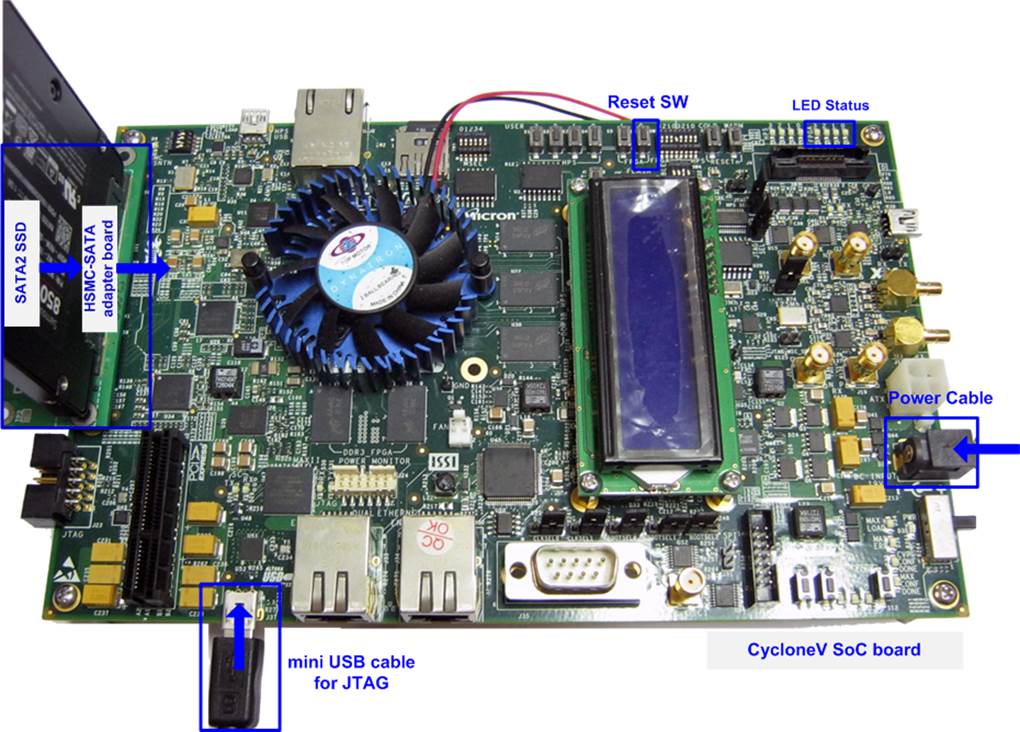
Figure 1‑1 SATA-IP host demo environment on CycloneV SX SoC development board
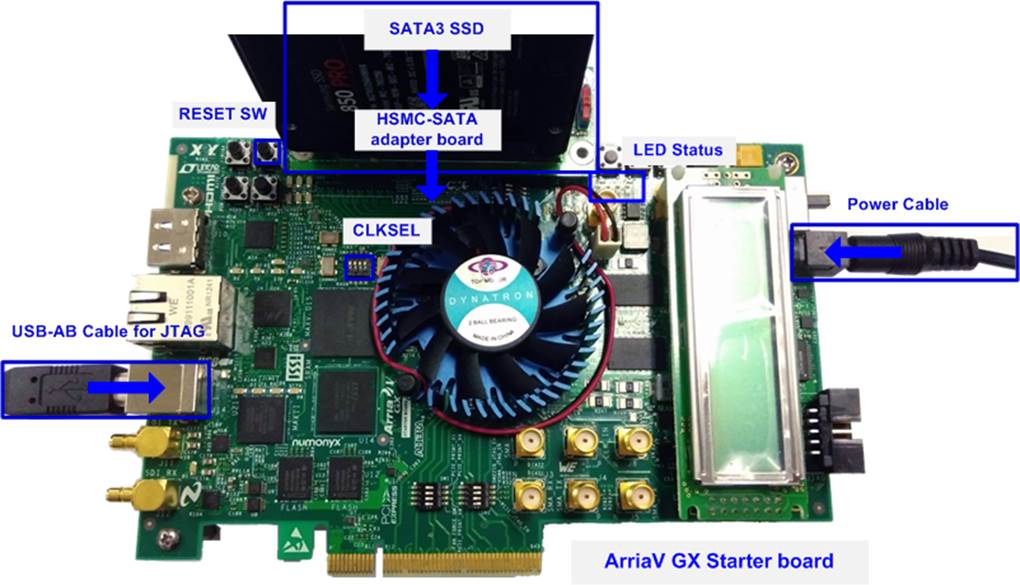
Figure 1‑2 SATA-IP host demo environment on ArriaV GX Starter board
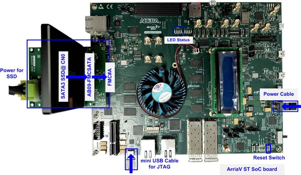
Figure 1‑3 SATA-IP host demo environment on ArriaV ST SoC development board
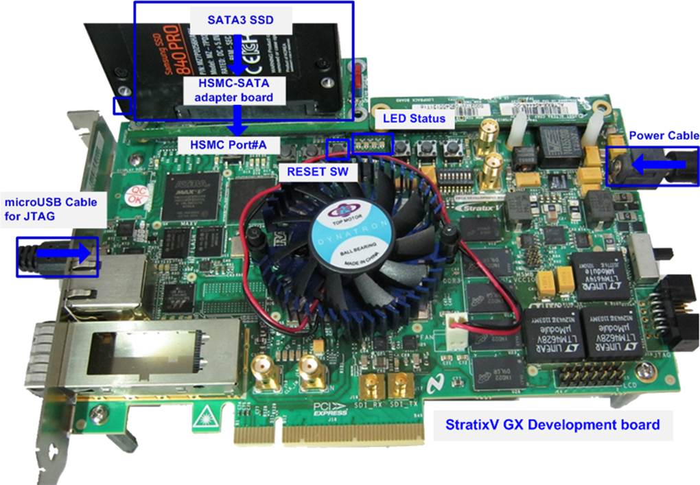
Figure 1‑4 SATA-IP host demo environment on StratixV GX development board
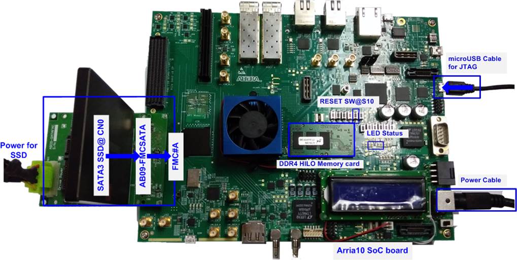
Figure 1‑5 SATA-IP host demo environment on Arria10 SoC development board
Following step is setup procedure for running demo.
- Power off FPGA board and adapter board.
- Connect HDD/SSD to SATA socket on CN0 @ HSMC/FMC SATA adapter board
a) For Cyclone V SoC board, insert SATA-II HDD/SSD.
b) For other boards, insert SATA-III HDD/SSD.
- For FMC adapter board, connect power to power connector on FMCSATA board.
- Connect SATA adapter board to FPGA board.
Note: If FPGA board has FMC/HSMC port more than one, use port#A.
- Connect USB A/B, USB mini, or USB micro cable between FPGA board and PC for JTAG programming and JTAG UART.
- Connect power supply to FPGA board.
- For CycloneV SX SoC/ArriaV ST SoC board, set JTAG enable at SW4 as shown in Figure 1‑6 to enable FPGA and MAX in JTAG chain.
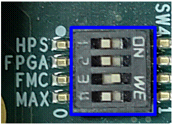
Figure 1‑6 Enable FPGA and MAX JTAG on CycloneV SoC and ArriaV SoC board
- Enable clock programmable for CycloneV SX SoC, ArriaV GX board
a) For CycloneV SX SoC board, set bit2 of SW2 to ON position.
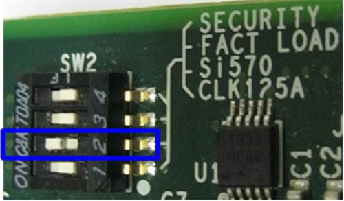
Figure 1‑7 Set SW to enable Si570 for CycloneV SX SoC board
b) For ArriaV GX board, set bit1 of SW4 to OFF position.
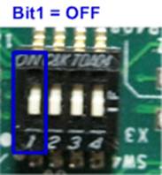
Figure 1‑8 Set SW to select clock input for ArriaV GX Starter board
- For Arria10 SoC board, remove boot card from the board and insert DDR4 HILO memory card to FPGA Memory.
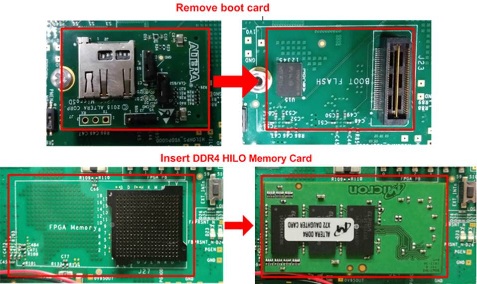
Figure 1‑9 Remove boot card and Insert DDR4 on Arria10 SoC board
- Power on FPGA board.
- Open “Clock Control” application to program clock for CycloneV SX SoC, ArriaV GX board, and StratixV GX board.
a) For CycloneV SX SoC board, select 1st tab (Si570), set Target frequency = 150 MHz, and click “Set New Frequency” button.
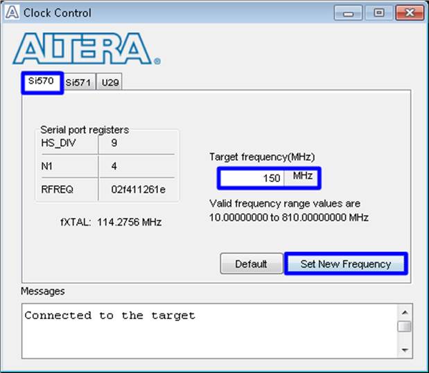
Figure 1‑10 Set clock frequency for CycloneV SX SoC board
b) For ArriaV GX board, select 1st tab (U4), set CLK0 frequency = 150 MHz, and click “Set New Frequency” button.
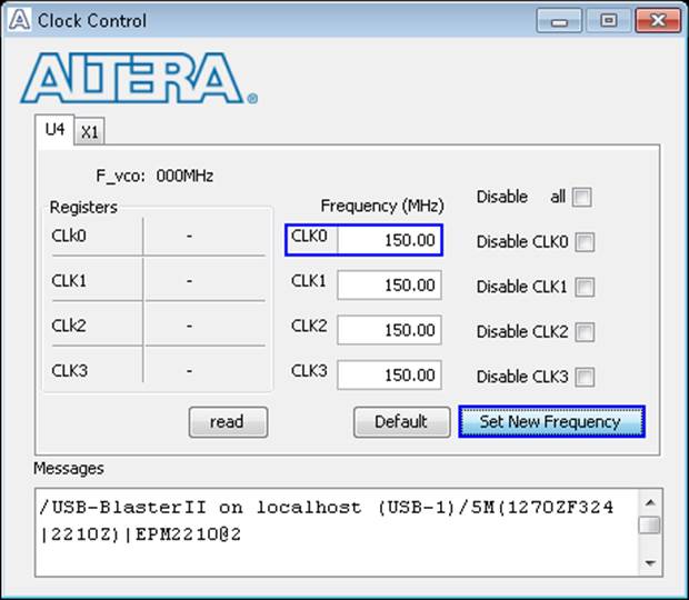
Figure 1‑11 Set clock frequency for ArriaV GX board
c) For StratixV GX board, select 3rd tab (U38), set CLK0 frequency = 150 MHz, and click “Set New Frequency” button.
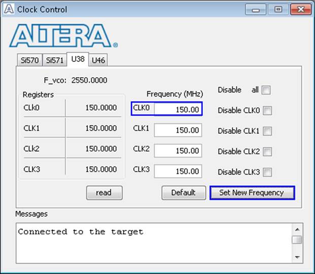
Figure 1‑12 Set clock frequency for StratixV GX board
- Open QuartusII Programmer and download SOF file to FPGA board, as shown in Figure 1‑13.
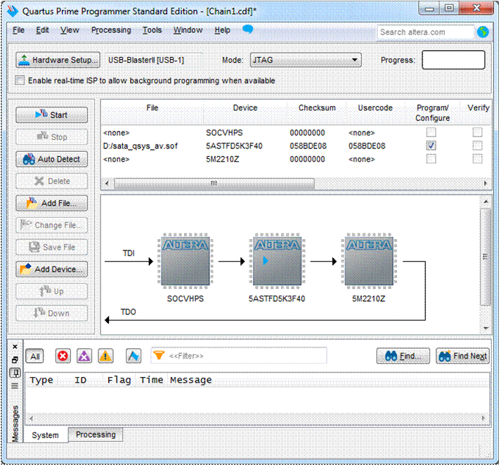
Figure 1‑13 Programmer Environment
- Power-on supply to SATA SSD.
a) For HSMC adapter, ON power-switch on HSMC adapter which is power supply for SATA SSD/HDD, as shown in Figure 1‑14.
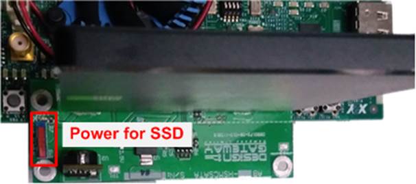
Figure 1‑14 Power switch on HSMC adapter
b) For FMC adapter, ON power supply which is connected to power connector on the adapter, as shown in Figure 1‑15.
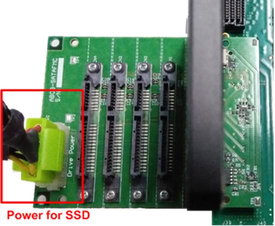
Figure 1‑15 Power for SSD on FMC adapter
- Check LED status on FPGA board now and LED0-1 should be ON, as shown in Figure 1‑16.
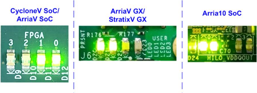
Figure 1‑16 LED Status after setup complete
|
LED |
ON |
OFF |
BLINK |
|
LED0 |
OK |
SATA-IP cannot detect SATA device. Please check SATA-cable connection or 150 MHz clock source. |
SATA-IP Error |
|
LED1 |
OK |
Internal PLL is not LOCK. |
SATA-IP Error |
|
LED2 |
In process of write SATA HDD/SSD |
Idle Status |
N/A |
|
LED3 |
In process of read SATA HDD/SSD |
Idle Status |
N/A |
Table 1 LED Status of host reference design
- Open NiosII Command Shell.
- Type “nios2-terminal” and then boot-up screen with Main menu for running SATA host demo is displayed, as shown in Figure 1‑17. More details about each Menu are described in next topic.
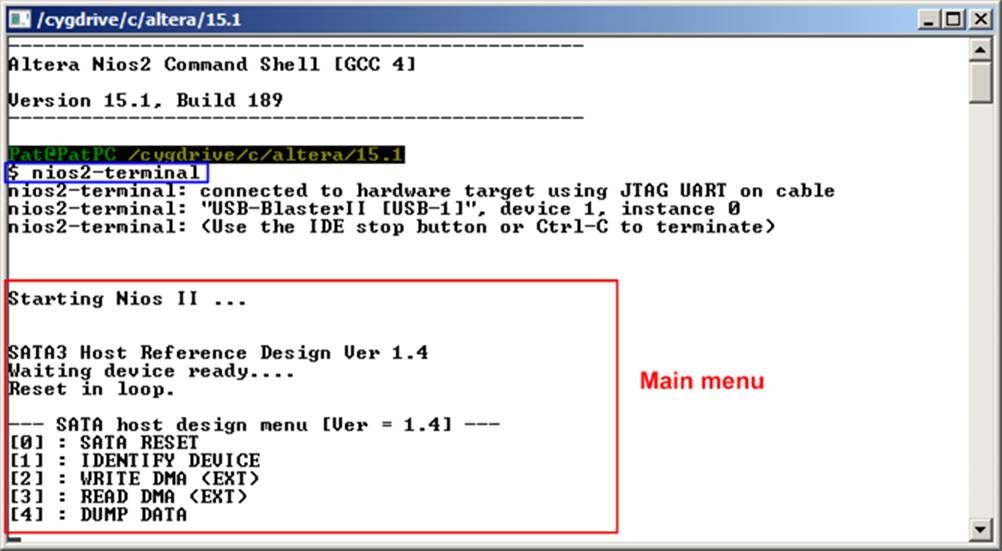
Figure 1‑17 Run NIOSII Terminal and boot-up screen
2 Main Menu
2.1 SATA RESET
Select ‘0’ for sending hardware reset signal to SATA-IP. Hardware reset is designed to reset both SATA-IP and SATA-PHY module. The system will re-initialize, and main menu will be displayed when complete reset sequence, as shown in Figure 2‑1.
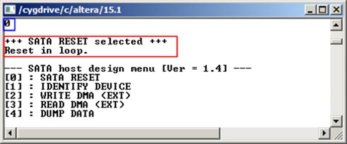
Figure 2‑1 SATA RESET Menu
2.2 IDENTIFY DEVICE
Select ‘1’ for sending “IDENTIFY DEVICE” command to HDD/SSD. Disk information (Model name, 48-bit LBA supported, disk capacity) will be displayed by using this menu, as shown in Figure 2‑2.
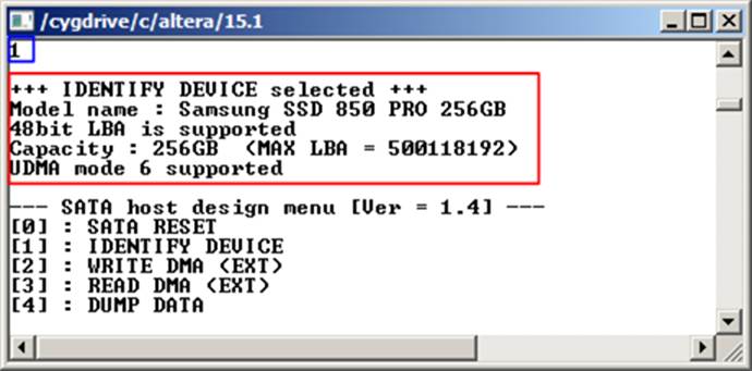
Figure 2‑2 IDENTIFY DEVICE Menu
2.3 WRITE DMA (EXT)
Select ‘2’ for sending “WRITE DMA (EXT)” command to HDD/SSD. Three inputs are required for this menu, i.e.
- Start LBA: this value is the start sector number of HDD/SSD to write data.
- Sector Count: this value is the total transfer size in sector unit (512 byte) for writing HDD/SSD. The data size which CPU filled to write buffer is equal to this input. If the input is more than 65536 (maximum size for one SATA command), only 65536 sector data is filled and the later command will use same data area with the first command.
- Write Pattern: this value is used for selecting test pattern to write to buffer and then forward to HDD/SSD. There are five test patterns in this demo, i.e. 32-bit increment [0], 32-bit decrement [1], 00000000H [2], FFFFFFFFH [3], and LFSR counter [4].
After Software receives all inputs correctly,
- “Prepare data” will be displayed during CPU writing test pattern data to write buffer.
- “Execute Write” will be displayed during CPU sending WRITE DMA (EXT) command and transferring data from write buffer to HDD/SSD.
- Transfer speed will be displayed after write operation complete.
Figure 2‑3 shows the example of test result when operation complete. Write operation will be cancelled when receiving error input as shown in Figure 2‑4.
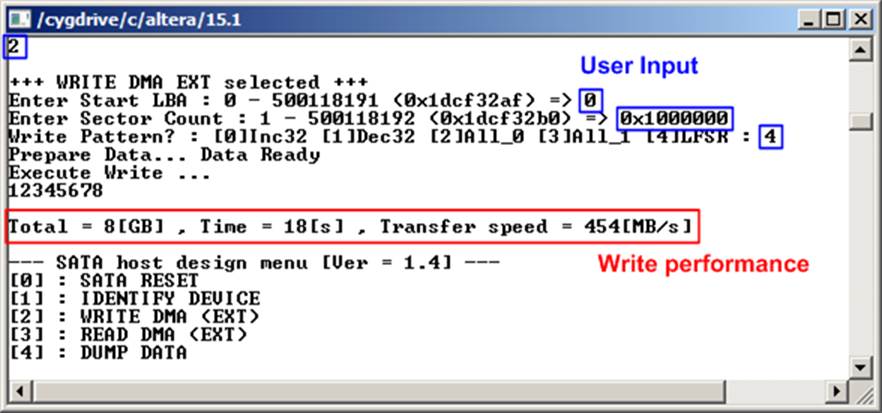
Figure 2‑3 WRITE DMA (EXT) command input and output
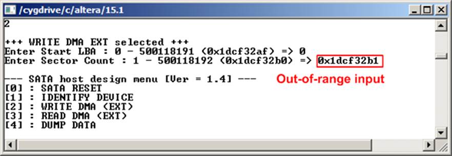
Figure 2‑4 Write operation cancelled from error input
2.4 READ DMA (EXT)
Select ‘3’ for sending “READ DMA (EXT)” command to HDD/SSD. Two or three inputs are required for this menu, i.e.
- Start LBA: same description with Start LBA in WRITE DMA (EXT) menu.
- Sector Count: same description with Sector Count in WRITE DMA (EXT) menu. If this input is not more than 65536, the third input will be displayed for selecting verification pattern. If input is more than 65536, the third input will not be displayed to skip data verification process and run for checking performance only, as shown in Figure 2‑5.
- Verify Pattern (Optional): this value is used for selecting verification pattern. This input should be matched with the pattern in WRITE DMA (EXT) menu. Five verification patterns can be selected, similar to write pattern. “Verify Data … Success” is displayed for success case, and “Data Mismatch with failure value” is displayed for failure case, as shown in Figure 2‑6 and Figure 2‑7 sequentially.
Similar to WRITE DMA (EXT) menu, Read operation will be cancelled if receiving error input as shown in Figure 2‑8.
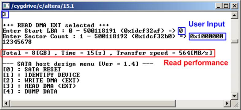
Figure 2‑5 READ COMMAND without Verify
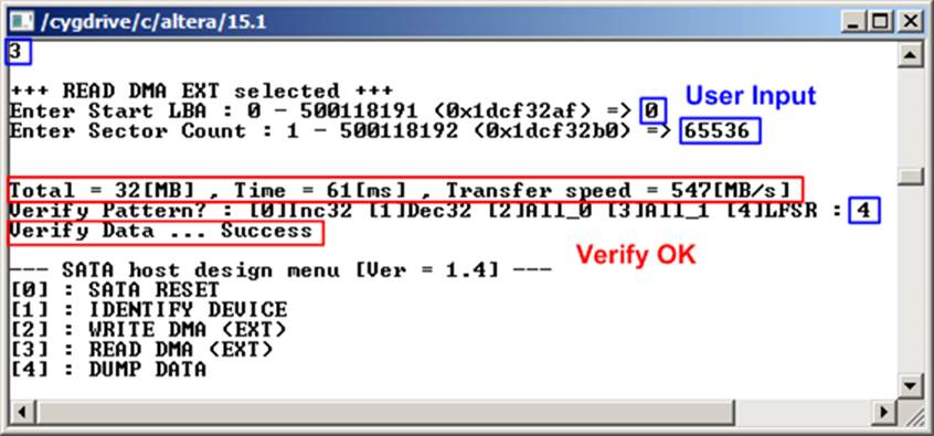
Figure 2‑6 READ COMMAND with verify successful
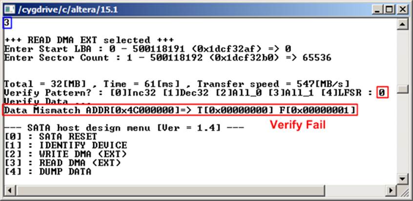
Figure 2‑7 READ COMMAND with verify failure
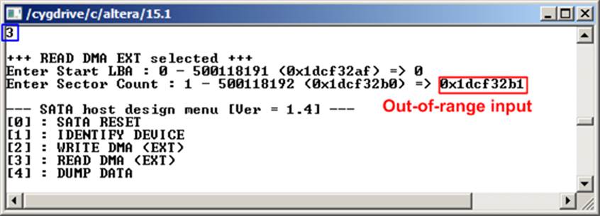
Figure 2‑8 Read operation cancelled from error input
2.5 DUMP DATA
Select ‘4’ to read data from DDR or read control register inside Avalon2SATA module for debugging. Two inputs are required for this menu, i.e.
- Start address: Heximal value can be input by adding prefix “0x”. Memory map of this reference design is displayed in Table 2.
- Byte length: Input read length in byte unit.
After setting all inputs, all read values will be displayed on console, as shown in Figure 2‑9.
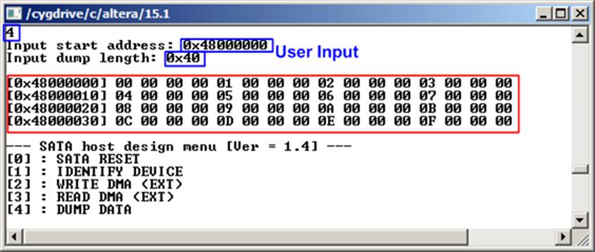
Figure 2‑9 DUMP DATA Menu
|
Address |
Memory map |
|
0x01000000-0x0100001F |
Avalon2SATA register area |
|
0x40000000-0x7FFFFFFF |
DDR memory area |
|
- 0x40000000-0x40000FFF |
TX FIS area |
|
- 0x40001000-0x40001FFF |
RX FIS area |
|
- 0x48000000-0x4BFFFFFF |
TX DATA FIS area |
|
- 0x4C000000-0x4FFFFFFF |
RX DATA FIS area |
Table 2 Memory map in NIOSII system
3 Revision History
|
Revision |
Date |
Description |
|
1.0 |
11-Mar-16 |
Initial version release |
|
2.0 |
5-Jul-16 |
Support Arria10 and merge V-series document |
|
2.1 |
1-Aug-16 |
Modify Figure 1‑5 to add DDR4 information |
|
2.2 |
11-Apr-17 |
- Update hardware setup on Arria10SOC - Add LED description |