Rev1.3 6-Jul-23
1 Environment Setup
To run the demo on IntelFPGA board, please prepare following environment.
1) IntelFPGA board:
- ArriaV GX Starter board
- Arria10 SoC Development board
- Alaric board from Reflex
- Arria10 GX Development board
2) PC with QuartusII programmer and NiosII command shell software
3) SATA adapter board
a) AB09-FMCRAID: For Arria10 SoC board/Arria10 GX board/Alaric board
b) AB12-HSMCRAID: For ArriaV GX board
4) SATA-III device
5) Power adapter for FPGA board and ATX power supply for SSD
6) USB cable for FPGA programming and NiosII command shell, connecting between FPGA board and PC
a) micro USB cable: For Arria10 SoC/Arria10 GX board/Alaric board
b) USB A-B cable: For ArriaV GX Starter board
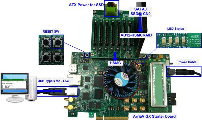
Figure 1‑1 HCTL-IP Demo Environment Setup on ArriaV GX Starter Board
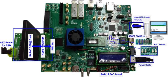
Figure 1‑2 HCTL-IP Demo Environment Setup on Arria10 SoC Development Board
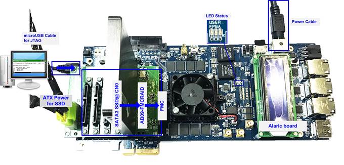
Figure 1‑3 HCTL-IP Demo Environment Setup on Alaric board
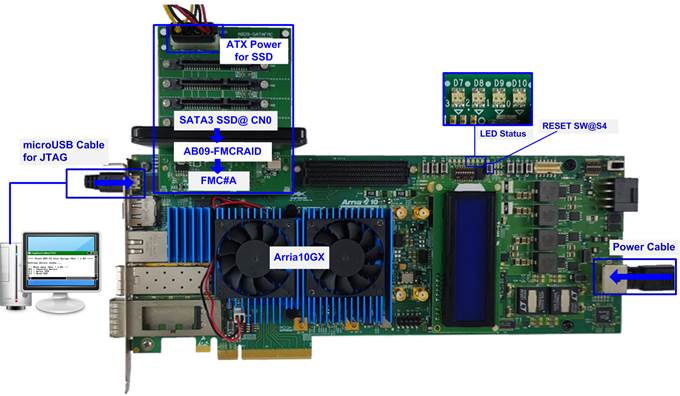
Figure 1‑4 HCTL-IP demo setup on Arria10 GX development board
2 Demo setup
1) Power off system.
2) Setup board option.
i) For ArriaV GX Starter board only, set bit1 of SW4 to OFF position.

Figure 2‑1 Set SW to select clock input for ArriaV GX Starter board
3) Setup SATA adapter board
i) For Arria 10 SoC Development board/Arria10 GX Development board/Alaric board: Connect AB09-FMCRAID to FMC#A
For ArriaV GX Starter board: Connect AB12-HSMCRAID to HSMC
ii) Connect SATA-III device to CN0 on AB09/AB12.
iii) Connect power to power connector on AB09/AB12.
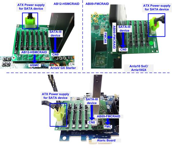
Figure 2‑2 AB09/AB12 connection to FPGA board
4) Connect USB cable from FPGA board to PC for JTAG programming and JTAG UART.
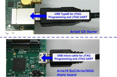
Figure 2‑3 micro USB cable for JTAG connection
5) Power on FPGA development board and power supply for SATA device.
6) Only ArriaV GX Starter board, open �Clock Control� application to program 150 MHz clock, as shown in Figure 2‑4. Select 1st tab (U4), set CLK0 frequency = 150 MHz, and click �Set New Frequency� button.
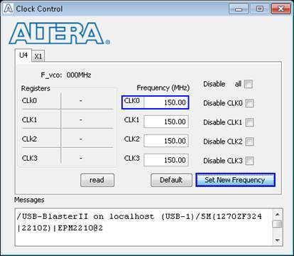
Figure 2‑4 Set clock frequency for ArriaV GX board
7) Open QuartusII Programmer to program �HSataIPTest.sof� file, as shown in Figure 2‑5.
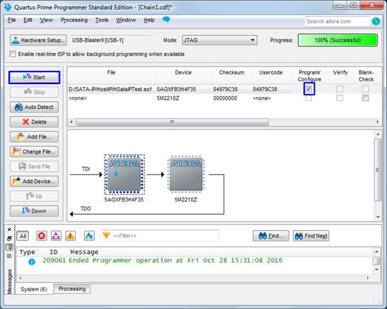
Figure 2‑5 Programmed by QuartusII Programmer
8) Open NiosII Command Shell and run nios2-terminal command. Boot message is displayed.
�Waiting device ready� is displayed during system initialization.
�SATA Gen3 Device Detect� is displayed after initialization is completed.
Finally, Main menu is displayed to receive command from user.
Figure 2‑6 NiosII Terminal
9) Check LED status on FPGA board. The description of LED is shown as follows.
Note: LED [3] is not available on Alaric board. There are three LEDs on the board.
Table 1 LED Definition
|
GPIO LED |
ON |
OFF |
|
0 |
Normal operation |
System is in reset condition |
|
1 |
System is busy |
Idle status |
|
2 |
Error detect |
Normal operation |
|
3 |
Data verification fail |
Normal operation |
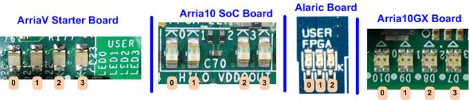
Figure 2‑7 LED Status after initialization complete
10) After programming completely, LED[0] and LED[1] are ON during SATA initialization process. LED[1] is OFF after SATA HCTL-IP completes initialization process and system is ready to receive command from user.

Figure 2‑8 LED status after program configuration file and SATA initialization complete
3 Test Menu
3.1 Identify Device
Select �0� to send Identify device command to SATA device. When the command operation is completed, the information of SATA device is displayed on the console.
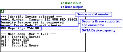
Figure 3‑1 Result from Identify Device menu
1) Device Model number: Show the SATA device model number connected to the board.
2) Security feature set: Supported or not supported. If the device is not supported, user must not run menu 3: Security erase command.
3) Normal Erase Mode Time: This is the estimation time to complete Security erase command. Minimum valid value is 2 minutes. This information is displayed when the device supports Security feature set.
4) Device capacity which is the output from HCTL-IP.
3.2 Write SSD
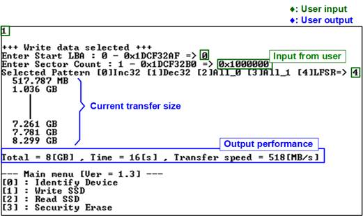
Figure 3‑2 Input and result of Write SSD menu
Select �1� to send Write command to SATA device. Three inputs are required for this menu.
1) Start LBA: Input start address of SATA device in 512-byte unit. The input is decimal unit when input only digit number. User can add �0x� as a prefix for hexadecimal input.
2) Sector Count: Input total transfer size in 512-byte unit. The input is decimal unit when input only digit number. User can add �0x� as a prefix for hexadecimal input.
3) Test pattern: Select test pattern of test data for writing to SATA device. Five patterns can be selected, i.e., 32-bit increment, 32-bit decrement, all 0, all 1, and 32-bit LFSR counter.
As shown in Figure 3‑2, if all inputs are valid, the operation is run. While operating Write command, the console displays the current amount of transferred data to indicate that the system is running. Finally, test performance, total size, and total time usage are displayed on the console as a test result.

Figure 3‑3 Example Test data in sector#0/#1 by increment/LFSR pattern
Test data of each 512-byte block has different 64-bit header which consists of 48-bit LBA address and 16-bit all 0 value. 48-bit LBA address is unique value for each 512-byte block. The data after 64-bit header is the test pattern which is selected by user. The example of test pattern is shown in Figure 3‑3. 32-bit incremental pattern is shown in the left window and 32-bit LFSR pattern is shown in the right window.
�Դ��Ҵ! ��辺���觡����ҧ�ԧ � �Դ��Ҵ! ��辺���觡����ҧ�ԧ show error message when user input is invalid. �Invalid input� is displayed on the console and then it returns to main menu to receive new command.
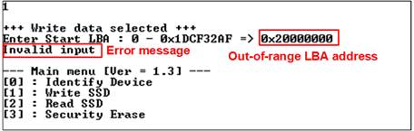
Figure 3‑4 Invalid Start LBA input
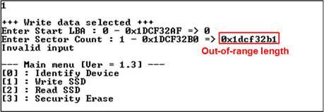
Figure 3‑5 Invalid Sector count input

Figure 3‑6 Invalid Test pattern input
3.3 Read SSD
Select �2� to send Read command to SATA device. Three inputs are required for this menu.
1) Start LBA: Input start address of SATA device in sector unit. The input is decimal unit when input only digit number. User can add �0x� as a prefix for hexadecimal input.
2) Sector Count: Input total transfer size in sector unit. The input is decimal unit when input only digit number. User can add �0x� as a prefix for hexadecimal unit.
3) Test pattern: Select test pattern to verify data from SATA device. Test pattern must be matched with the test pattern using in Write Command menu. Five patterns can be selected, i.e., 32-bit increment, 32-bit decrement, all 0, all 1, and 32-bit LFSR counter.

Figure 3‑7 Input and result of Read SSD menu
When all inputs in the Read command menu are valid, the test system starts reading data from the SATA device. While operating Read command, the console displays the amount of transferred data every second. Upon completion of the data transfer, the test performance, total size, and time usage are displayed as a test result. However, if some inputs are out-of-range, the console displays �Invalid input�.
Figure 3‑8 and Figure 3‑9 show the error message when data verification is failed. �Verify fail� is displayed with error address, expected data, and read data. User can press any key to cancel read operation or wait until the read operation is done.
In case of cancel operation, the previous command does not complete in a good sequence. It is recommended to power-off/on SATA device and press �RESET� button to restart system.

Figure 3‑8 Data verification is failed but wait until read complete
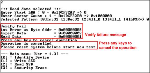
Figure 3‑9 Data verification is failed and press key to cancel operation
3.4 Security Erase
Select �3� to send Security Erase command to SATA Device. Please confirm that SATA device supports Security Erase feature using Identify device menu. The estimated time of security erase operation is also displayed in Identify device menu.
After selecting the menu, confirmation message is displayed on the console. User inputs �y� or �Y� to continue Security erase operation or inputs other keys to cancel operation.
While operating this command, the console displays an incremental number every second to indicate that the command is operating. After the operation is completed, total time usage is displayed as a test result.
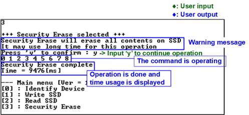
Figure 3‑10 Result from Security Erase command
Figure 3‑11 shows the example when user inputs other keys to cancel the command.
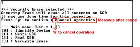
Figure 3‑11 Cancel Security Erase command
4 Revision History
|
Revision |
Date |
Description |
|
1.3 |
27-Feb-23 |
Support A10GX |
|
1.2 |
15-Nov-17 |
Add LFSR pattern and Alaric board |
|
1.1 |
24-Nov-16 |
Correct security erase menu |
|
1.0 |
28-Oct-16 |
Initial version release |