HCTL-IP reference design manual
Rev1.3 22-Aug-23
1 Introduction

Figure 1‑1 HCTL-IP hardware comparing to SATA-IP hardware
The SATA-IP reference design utilizes CPU firmware to handle the application layer and DDR to store the SATA FIS packet transferred between the CPU and SATA-IP. As a result, the system requires both CPU and DDR to operate the SATA protocol. However, if the system uses HCTL-IP, a hardware solution for handling the SATA application layer, it can be designed to control the SATA device without using CPU and DDR. Users can design the logic for connecting with HCTL-IP by utilizing a simple state machine for Control I/F and FIFO for Data I/F.
The advantage of using CPU with SATA-IP is the system�s flexibility, allowing for updates through CPU firmware. This means that the supported ATA commands can be easily upgraded. In contrast, using HCTL-IP, which is hardwired logic, limits the supported ATA command to four commands, i.e., Identify device, Security erase, Write, and Read
The advantage of using HCTL-IP that it utilizes small resources while providing higher performance, compared to using CPU and DDR. CPU system and DDR require a lot of logics and the CPU must handle many tasks, including SATA application, resulting in overhead time from task switching. The test result from running Write command on the HCTL-IP reference design shows better speed than the SATA-IP reference design that uses CPU and DDR.
More details of SATA-IP reference design are described in following documents.
https://dgway.com/products/IP/SATA-IP/Altera/dg_sata_ip_datasheet_altera5_en.pdf
https://dgway.com/products/IP/SATA-IP/Altera/dg_sata_host_refdesign_altera5_en.pdf
2 Hardware overview
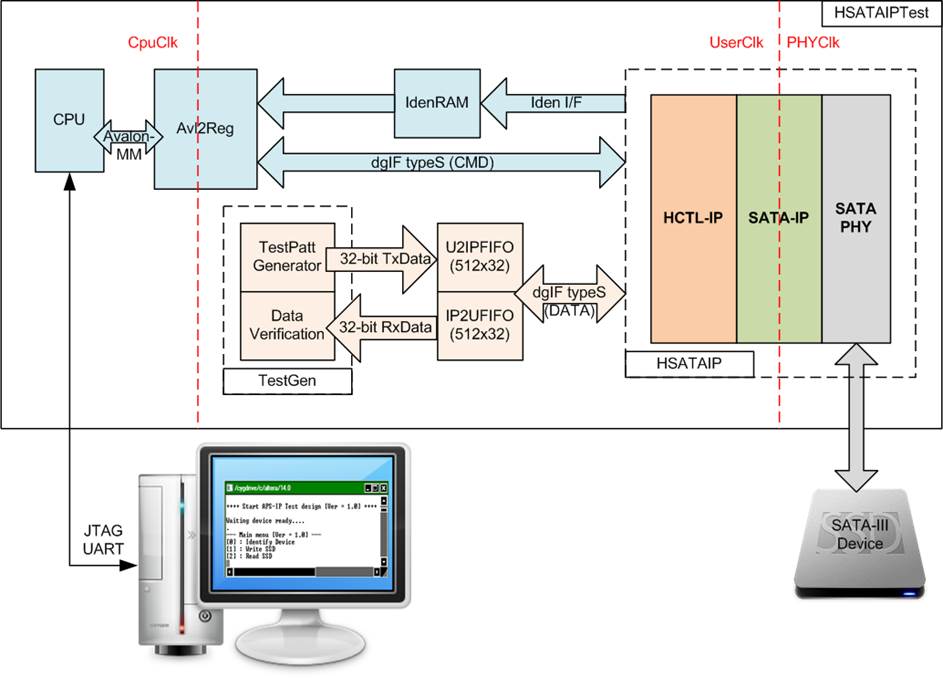
Figure 2‑1 HCTL-IP demo hardware
The hardware system can be categorized into three groups.
1) TestGen: This module is an example of user logic to write and read data with HCTL-IP. When running Write command, TestGen generates test data at the highest speed with flow control and sends it to U2IPFIFO. For the Read command, TestGen reads and verifies test data from IP2UFIFO at the highest speed with flow control. TestGen uses a 32-bit data bus and runs in the UserClk domain, which is equal to 200 MHz, resulting in a maximum bandwidth of 800 MB/s. This is higher than the maximum performance of SATA-III devices.
2) SATA: HCTL-IP connects with SATA-IP and SATA PHY to perform host operations with SATA devices. The user interface of HCTL-IP, called �dgIF typeS�, is a standard interface of storage IP by Design Gateway. It comprises the Command interface and Data interface. When operating the Identify device command, the Iden I/F transfers the Identify device data to a simple dual-port RAM.
3) CPU: The user controls the test operation in the demo through JTAG UART. The test parameters and operation set by the user on the console are handled by CPU firmware. The hardware receives the test parameters processed by CPU through Avalon-MM bus. Avl2Reg has registers to store test parameters mapped to different addresses, including the address decoder to select the correct parameter that CPU sends write requests. Additionally, the hardware status and other parameters are mapped to different addresses for CPU reading and monitoring. While operating the test, CPU reads and displays the test progress and status on the JTAG UART.
More details of the hardware are described as follows.
2.1 TestGen
The TestGen module generates a Test pattern to be the transmitted data for WrFf in Write command or the expected data to be compared with the received data from RdFf in Read command. It operates at the highest possible speed to evaluate the system�s performance. The details of hardware inside TestGen are shown in Figure 2‑2.
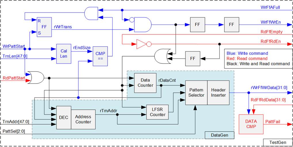
Figure 2‑2 TestGen hardware

Figure 2‑3 Timing diagram of Write operation in TestGen
In order to execute a Write command, WrPattStart from Avl2Reg is set to 1b for one clock cycle. After that, rWrTrans is set to 1b until the write operation is done. The FIFO Write enable (rWrFfWrEn[0]) is set to 1b to send test data to WrFf when rWrTrans=1b and WrFfAFull=0b. If FIFO is almost full (WrFfAFull=1b), rWrFfWrEn[0] is set to 0b to pause data transmission. rDataCnt is the data counter to keep track of the amount of transferred data. It is incremented when rWrFfWrEn[0] is set to 1b. After all data is transferred (rDataCnt=rEndSize), rWrTrans and rWrFfWrEn[0] are de-asserted to 0b to stop transferring data. rEndSize indicates the total transfer size in 512-byte unit, which is calculated by TrnLen signal (the input by the user).
To execute a Read command, the RdFfRdEn is designed by connecting NOT logic to RdFfEmpty. Therefore, data is always read from RdFf by asserting RdFfRdEn to 1b when the data is available (RdFfEmpty=0b). rDataCnt is incremented when RdFfRdEn is asserted to 1b. rDataCnt is applied to generate test data which is the expected value for verifying the received data (RdFfRdData).
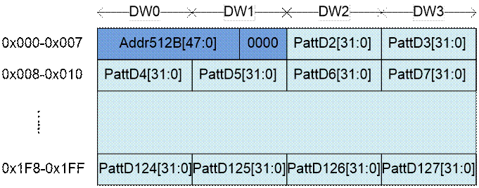
Figure 2‑4 Test pattern format in each sector
The �DataGen� block in the lower side of Figure 2‑2 shows the logic for generating test pattern in the TestGen module. To create a unique test data for each 512-byte data, the test pattern is designed as shown in Figure 2‑4.
The test pattern consists of two parts: 64-bit header in Dword#0 and Dword#1 of each 512-byte block and test data in Dword#2 � Dword#127. The 64-bit header is created using the LBA address (the address in 512-byte unit). As shown in Figure 2‑2, TrnAddr is loaded to be the initial value of rTrnAddr. which is used as the 64-bit header of each 512-byte data. rTrnAddr is incremented after transferring the last data of each 512-byte block. The last data of each 512-byte block can be monitored from rDataCnt with the write/read enable.
TestGen supports to generate five patterns, i.e., 32-bit incremental, 32-bit decremental, all 0, all 1, and 32-bit LFSR. 32-bit incremental data is created by using the lower bits of rTrnAddr and rDataCnt. While the Decremental data utilizes NOT logic connected with the incremental data. The 32-bit LFSR counter uses the 1st DW data (LBA[31:0]) to be the initial value for generating a test pattern in each 512-byte data. The LFST equation is x^31 + x^21 + x + 1.
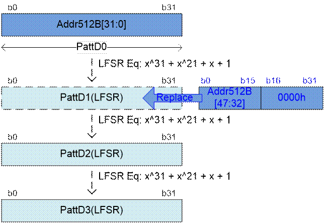
Figure 2‑5 LFSR pattern in TestGen
A 3-bit PattSel signal is utilized to select one of five test patterns. The Header Inserter logic inserts a 64-bit header to be the first and the second data of each 512-byte block. After that, test data from the pattern counter is transferred to rWrFfWrData. In the Read command, rWrFfWrData is used as the expected value to compare with the read data from the FIFO (RdFfRdData). PattFail is asserted to 1b when data verification fails.
2.2 SATA
The user interface of HCTL-IP uses dgIF typeS interface. The command interface is connected to Avl2Reg for configuring test parameters and reading system status through JTAG UART. Additionally, the 32-bit data interface is connected to both U2IPFIFO and IP2UFIFO. HCLT-IP is integrated with SATA-IP and SATA PHY to handle SATA host operation with SATA device, as shown in Figure 2‑6.
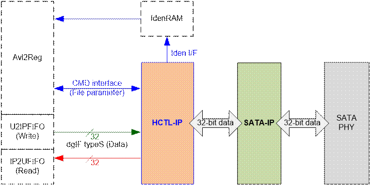
Figure 2‑6 SATA hardware
2.2.1 HCTL-IP
HCTL-IP implements the application layer of the SATA protocol to generate and decode SATA FIS packets with SATA-IP. It supports four commands: Identify device, Security erase, Write, and Read. For further details, please refer to the datasheet.
https://dgway.com/products/IP/SATA-IP/Altera/dg_sata_host_ip_datasheet_alt_en.pdf
2.2.2 SATA-IP
SATA-IP implements a part of transport layer and link layer of SATA protocol. It includes two asynchronous FIFOs for transferring data stream across clock domains between the user interface and PHY interface in both transfer directions. Please refer to the SATA-IP datasheet for more information.
https://dgway.com/products/IP/SATA-IP/Altera/dg_sata_ip_datasheet_altera5_en.pdf
2.2.3 SATA PHY
The logic of this module provides an example of an HDL that includes the state machine for controlling the OOB (Out-of-band) sequence of the SATA host operation. Additionally, it includes the transceiver, which is dependent on the FPGA model. More details of SATA PHY are described in SATA-IP reference design.
https://dgway.com/products/IP/SATA-IP/Altera/dg_sata_host_refdesign_altera5_en.pdf
2.3 CPU and Peripherals
The hardware connects to CPU via Avalon-MM bus, similar to other CPU peripherals. The hardware registers are mapped to CPU memory address, as shown in Table 2‑1. Avl2Reg is the hardware module that consists of the control and status registers for CPU access via the Avalon-MM bus.
The signal interface of TestGen, HCTL-IP, and IdenRAM are connected to Avl2Reg for parameter assignment and status monitoring. As shown in Figure 2‑7, there are two clock domains used in this block: CpuClk (the CPU system clock for Avalon-MM interface) and UserClk (the user clock domain of TestGen and HCTL-IP). More information of each hardware is described below.

Figure 2‑7 CPU and peripherals hardware
2.3.1 AsyncAvlReg
The purpose of this module is to convert the signal interface of Avalon-MM to a Register interface, as well as to transfer signals between the CpuClk domain and the UserClk domain. The timing diagram of the Register interface is shown in Figure 2‑8.
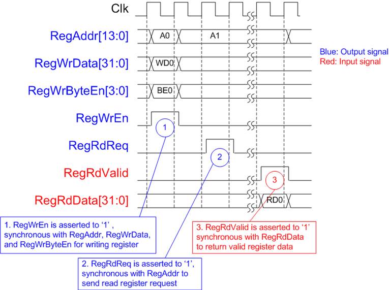
Figure 2‑8 Register interface timing diagram
To write to the register, the timing diagram is similar to RAM interface. RegWrEn is asserted to 1b along with the valid signal of RegAddr (Register address in 32-bit unit), RegWrData (write data of the register), and RegWrByteEn (bit[0], [1], [2], and [3] are write enable for RegWrData[7:0], [15:8], [23:16], and bit[31:24]).
To read from the register, AsyncAvlReg asserts RegRdReq to 1b with the valid value of RegAddr (the register address used for 32-bit unit). The module waits until RegRdValid is asserted to 1b which indicates the validity of the RegRdData signal. When performing a read access, RegAddr retains the same value until RegRdValid is asserted to 1b.
2.3.2 UserReg
Figure 2‑7 shows that the interface of UserReg and AsyncAvlReg is a Register interface. The Address decoder decodes the address in the command request to select the active register for Write access or Read access. When a Write request is received, RegWrData is loaded to the active register. In this reference design, UserReg does not use RegWrByteEn because CPU firmware always uses a 32-bit pointer to set the parameters to the hardware register.
For a Read request, the status signals for CPU access from TestGen, HCTL-IP, and IdenRAM are mapped to the Data multiplexer with pipelines registers. The read data is selected by decoding the RegAddr value. The latency time of the RegRdData, which is the output of the Data multiplexer, is one clock cycle. Therefore, RegRdValid is designed by using a D Flip-flop, input by RegRdReq signal.
The memory map of the control and status signals inside the UserReg module is shown in Table 2‑1.
Table 2‑1 Register Map
|
Address |
Register Name |
Description |
|
Rd/Wr |
(Label in the �hsataiptest.c�) |
|
|
BA+0x000 |
User Address (Low) Reg |
[31:0]: Input to be start address as 512-byte unit (UserAddr[31:0] of dgIF typeS for HCTL-IP) |
|
Wr |
(USRADRL_REG) |
|
|
BA+0x004 |
User Address (High) Reg |
[15:0]: Input to be start address as 512-byte unit (UserAddr[47:32] of dgIF typeS for HCTL-IP) |
|
Wr |
(USRADRH_REG) |
|
|
BA+0x008 |
User Length (Low) Reg |
[31:0]: Input to be transfer length as 512-byte unit (UserLen[31:0] of dgIF typeS for HCTL-IP) |
|
Wr |
(USRLENL_REG) |
|
|
BA+0x00C |
User Length (High) Reg |
[15:0]: Input to be transfer length as 512-byte unit (UserLen[47:32] of dgIF typeS for HCTL-IP) |
|
Wr |
(USRLENH_REG) |
|
|
BA+0x010 |
User Command Reg |
[1:0]: Input to be user command (UserCmd of dgIF typeS for HCTL-IP) 00b-Identify device, 01b-Security erase, 10b-Write Dev, 11b-Read Dev When this register is written, the command request to HCTL-IP is asserted to start the command operation. |
|
Wr |
(USRCMD_REG) |
|
|
BA+0x014 |
Test Pattern Reg |
[2:0]: Test pattern select 000b-Increment, 001b-Decrement, 010b-All 0, 011b-All 1, 100b-LFSR |
|
Wr |
(PATTSEL_REG) |
|
|
BA+0x100 |
User Status Reg |
[0]: UserBusy of dgIF typeS for HCTL-IP (0b: Idle, 1b: Busy) [1]: UserError of dgIF typeS for HCTL-IP (0b: Normal, 1b: Error) [2]: Data verification fail (0b: Normal, 1b: Error) [4:3]: SATA speed from IP 00b: No linkup, 01b: SATA Gen1 (Not supported), 10b: SATA Gen2, 11b: SATA Gen3 |
|
Rd |
(USRSTS_REG) |
|
|
BA+0x104 |
Total disk size (Low) Reg |
[31:0]: Total capacity of SATA device in 512-byte unit (LBASize[31:0] of dgIF typeS for HCTL-IP) |
|
Rd |
(LBASIZEL_REG) |
|
|
BA+0x108 |
Total disk size (High) Reg |
[15:0]: Total capacity of SATA device in 512-byte unit (LBASize[47:32] of dgIF typeS for HCTL-IP) |
|
Rd |
(LBASIZEH_REG) |
|
|
BA+0x10C |
User Error Type Reg |
[31:0]: User error status, directly mapped from UserErrorType[31:0] of HCTL-IP. |
|
Rd |
(USRERRTYPE_REG) |
|
|
BA+0x11C |
SATA HCTL IP Test pin Reg |
[31:0]: TestPin[31:0] which is directly mapped from HCTL-IP |
|
Rd |
(TESTPIN_REG) |
|
|
BA+0x120 |
Data Failure Address (Low) Reg |
[31:0]: Latch value of failure address [31:0] in byte unit from Read command |
|
Rd |
(RDFAILNOL_REG) |
|
|
BA+0x124 |
Data Failure Address (High) Reg |
[24:0]: Latch value of failure address [56:32] in byte unit from read command |
|
Rd |
(RDFAILNOH_REG) |
|
|
BA+0x130 |
Expected value Word0 Reg |
[31:0]: Latch value of expected data [31:0] from Read command |
|
Rd |
(EXPPATW0_REG) |
|
|
BA+0x140 |
Read value Word0 Reg |
[31:0]: Latch value of read data [31:0] from Read command |
|
Rd |
(RDPATW0_REG) |
|
|
BA+0x150 |
Current test byte (Low) Reg |
[31:0]: Current amount of transferred data inside TestGen module in byte unit (bit[31:0]) |
|
Rd |
(CURTESTSIZEL_REG) |
|
|
BA+0x154 |
Current test byte (High) Reg |
[24:0]: Current amount of transferred data inside TestGen module in byte unit (bit[56:32]) |
|
Rd |
(CURTESTSIZEH_REG) |
|
|
BA+0x2000 � BA +0x21FF |
Identify Device Command Data (IDENCTRL_REG) |
512-byte Identify Device Data |
3 CPU Firmware
Upon system boot-up, the CPU initializes its peripherals, including JTAG UART and Timer. The CPU then waits for the HCTL-IP to complete the initialization process, indicated by USRSTS_REG[0]=0b before displaying the main menu. The CPU firmware supports four commands based on the USRCMD_REG value: Identify device (00b), Security erase (01b), Write (10b), and Read (11b). The sequence for each command is described below.
3.1 Identify device command
When user selects the Identify device command, the firmware executes the following sequence.
1) Set USRCMD_REG=00b and send the Identify device command to HCTL-IP via Test logic. The HCTL-IP busy flag (USRSTS_REG[0]) changes from 0b to 1b.
2) Wait for the operation to completed or detect errors by monitoring USRSTS_REG value.
Bit[0] is de-asserted to 0b when the command is completed. After the command is completed, the data from the Identify device command of the SATA device is stored in IdenRAM.
Bit[1] is asserted to 1b if errors are detected. Then, an error message will be displayed on the console.
3) Read the Identify device data from IdenRAM, which is mapped to IDENCTRL_REG address. The CPU then displays the information such as SATA device model name, security feature set supported, and erase time value on JTAG UART. Additionally, the device capacity (LBASIZEL/H_REG) is displayed in GB unit on the console.
3.2 Write/Read command
When the user selects the Write/Read command, the firmware executes the following sequence.
1) Receive start address, transfer length, and test pattern through JTAG UART. If any inputs are invalid, the operation is cancelled.
2) Set the value of USRADRL/H_REG, USRLENL/H_REG, PATTSEL_REG, and USRCMD_REG (USRCMD_REG=10b for write command and 11b for read command) to match the received inputs.
3) Waits for the operation to completed or detects errors (except verification error) monitoring USRSTS_REG[2:0]. If USRSTS_REG[2] is asserted to 1b, indicating a verification error, an error message is displayed, but the operation continues. If the user enters any keys to the console after detecting the verification error, the operation is cancelled.
4) While the command operation is ongoing, the current amount of transferred data reading from CURTESTSIZE_REG is displayed every second. Finally, test performance is displayed on JTAG UART when the command is completed.
3.3 Security erase command
When the user selects the Security erase command, the firmware executes the following sequence.
1) Set USRCMD_REG=01b and send the Security erase command to HCTL-IP via the Test logic. The HCTL-IP busy flag (USRSTS_REG[0]) changes from 0b to 1b.
2) Wait for the command operation to complete by monitoring USRSTS_REG value until Bit[0] is de-asserted to 0b. Since this operation may take a long time, a dummy message is displayed on the console every second to show system alive status. Finally, the total time usage is displayed on JTAG UART when command is completed.
4 Example Test Result
Figure 4‑1 shows an example test result when running demo system using a 256 GB Samsung 860 Pro.

Figure 4‑1 Test Performance of SATA HCTL IP demo by using Samsung 860 Pro SSD
At SATA Gen3 speed, the write performance is about 525 Mbyte/sec while the read performance is about 563 Mbyte/sec.
5 Revision History
|
Revision |
Date |
Description |
|
1.3 |
27-Feb-23 |
Update the details of reference design |
|
1.2 |
14-Nov-17 |
Add LFSR pattern |
|
1.1 |
24-Jan-17 |
Update signal to dgIF typeS |
|
1.0 |
28-Oct-16 |
Initial Release |
Copyright: 2016 Design Gateway Co,Ltd.