1 Environment Requirement
To run the demo on FPGA board, please prepare the following hardware/software.
1) IntelFPGA board: Arria10 SoC or Arria10 GX Development board
2) PC installing QuartusII programmer and NiosII command shell software
3) AB09-FMCRAID board, provided by Design Gateway
4) ATX power supply connecting to power connector on FMCRAID board for SATA device power
5) Eight SATA-III devices, inserting to CN0-CN7 of FMCRAID board
6) FPGA power adapter for FPGA board
7) Micro USB cable for programming FPGA and NiosII command shell, connecting between FPGA board and PC

Figure 1‑1 HCTL-IP RAID0 demo environment setup on Arria10 SoC board
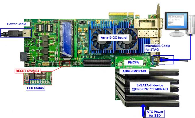
Figure 1‑2 HCTL-IP RAID0 demo environment setup on Arria10 GX board
2 Demo setup
1) Power off system.
2) Connect AB09-FMCRAID as shown in Figure 2‑1.
i. Connect AB09-FMCRAID to FMC#B for Arria10 SoC board or FMC#A for Arria10 GX board.
ii. Connect eight SATA-III devices to CN0-CN7 on AB09-FMCRAID board.
iii. Connect ATX power to power connector on AB09.

Figure 2‑1 AB09 connection to FPGA board
3) Connect micro USB cable from FPGA board to PC for JTAG programming and JTAG UART.
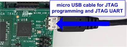
Figure 2‑2 USB cable for JTAG connection
4) Power on FPGA development board and ATX power supply for SATA device.
5) Use QuartusII Programmer to program �HSATARaid0x8.sof� file, as shown in Figure 2‑3.
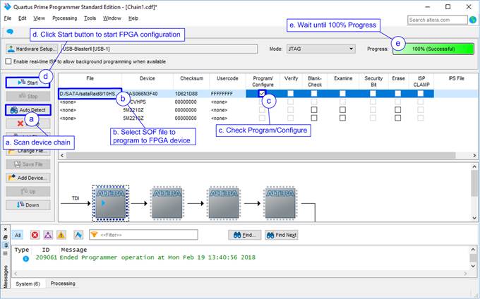
Figure 2‑3 Programmed by QuartusII Programmer
6) Open NiosII Command Shell and run nios2-terminal command. After that, boot message is displayed.
- �Waiting device ready� message is displayed during system initialization.
- �SATA Gen3 Device Detect� shows SATA speed after complete RAID0 initialization.
- Main menu is displayed to receive command from user.
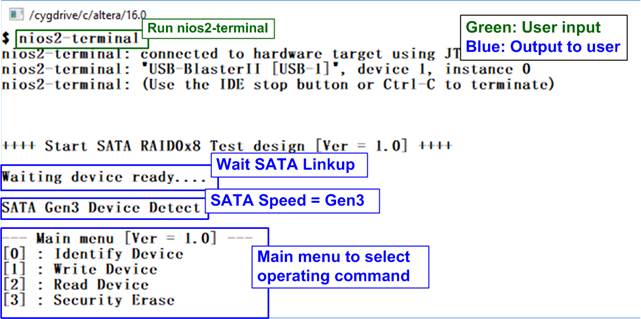
Figure 2‑4 NiosII Terminal after boot up
7) If some SATA devices are not detected, �CH[X] Not Detect� will be displayed as shown in Figure 2‑5. X is referred to SATA channel number which has found the error. Please check SATA device in the error channel.
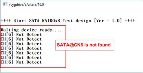
Figure 2‑5 Error message when some devices are not detected
8) Check LED status on FPGA board. The description of LED is shown in Table 2‑1.
Table 2‑1 LED Definition
|
GPIO LED |
ON |
OFF |
|
0 |
Normal operation |
System is in reset condition |
|
1 |
System is busy |
Idle status |
|
2 |
Error detect |
Normal operation |
|
3 |
Data verification fail |
Normal operation |
9) After programming completely, LED[0] and LED[1] are ON during RAID0 initialization process. LED[1] changes to OFF after RAID0 finishes initialization process. Now the system is ready to receive new command from user.
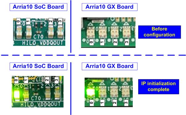
Figure 2‑6 LED status
3 Test Menu
3.1 Identify Device
Select �0� to send Identify device command to RAID0.
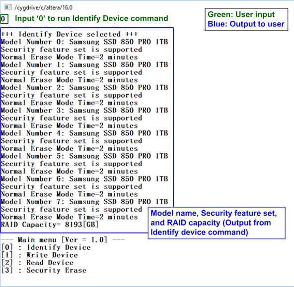
Figure 3‑1 Test result when running Identify device menu
When the operation is completed, the device information is displayed on NiosII command shell. The console shows four values.
1) SSD model number: This value is decoded from Identify device data.
2) Security feature: This value is decoded from Identify device data to check that the device supports to run menu 3 (Security erase command) or not.
3) Normal Erase Mode Time: This value is decoded from Identify device data to check the estimation time to complete Security erase command. The minimum value is 2 minutes. This information is displayed when the device supports Security feature set.
4) SSD capacity: This value is signal output from RAID0 block. The value is equal to eight times of SATA CH#0 capacity.
3.2 Write Device
Select �1� to send Write command to RAID0.
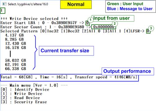
Figure 3‑2 Test result when running Write command
Three inputs are required for this menu.
1) Start LBA: Input start address to write RAID0 as 512 byte unit. The input is decimal unit when input only digit number. User can add �0x� to be prefix when input is hexadecimal unit.
2) Sector Count: Input total transfer size as 512 byte unit. The input is decimal unit when input only digit number. User can add �0x� to be prefix when input is hexadecimal unit.
3) Test pattern: Select test data pattern for writing to RAID0. Five patterns can be selected, i.e. 32-bit increment, 32-bit decrement, all 0, all 1, and 32-bit LFSR counter.
If all inputs are valid, the operation will be started. During writing data, current transfer size is displayed on the console every second to show that system is still alive. Finally, total size, total time usage, and test speed are displayed on the console as test result.
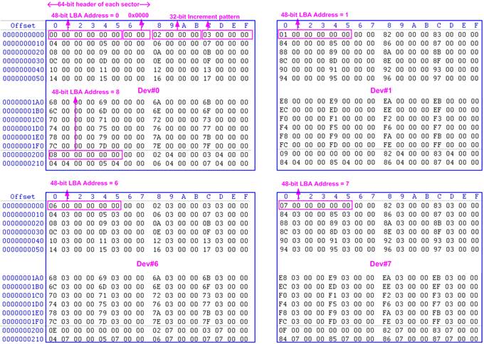
Figure 3‑3 Example Test data in sector#0/#1 of devices by increment pattern
Test data is split into 512 byte unit. Each 512 byte data has unique 64 bit header which consists of 48 bit address (in 512 byte unit) and 16 bit zero value. The data after 64 bit header is the test pattern which is selected by the user.
Figure 3‑3 shows the example when using 32 bit increment pattern. The stripe size of RAID0 demo is 512 byte. So, the data is switched to the next device when finishing each 512 byte data. The test data sequence is arranged from Disk#0, #1, �, #7, and then skips to the next 512 byte address of Disk#0, #1, � #7, and so on. The header shows the address of test data in 512 byte unit. To calculate the disk number from the test data address, the following equation can be applied.
Device number = <Test data address in 512 byte unit> mod 8.
Dev#0 stores test data address = 0, 8, 16, �
Dev#1 stores test data address = 1, 9, 17, �
�
Dev#7 stores test data address = 7, 15, 23, �
The test data address could be checked from 48 bit address in the header of each 512 byte unit data in the device.
Figure 3‑4 shows the example when the input is less than or more than the recommended range for each parameter. The console displays �Invalid input� and then the operation is cancelled.
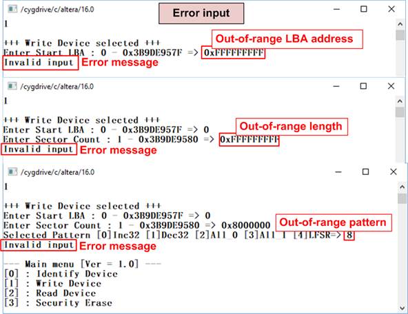
Figure 3‑4 Error message when the input is invalid
3.3 Read Device
Select �2� to send Read command to RAID0.
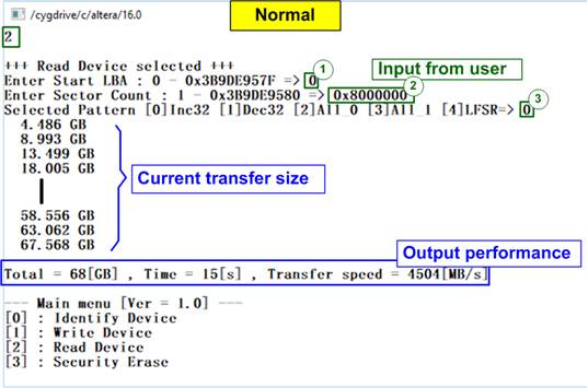
Figure 3‑5 Test result when running Read command
Three inputs are required for this menu.
1) Start LBA: Input start address to read RAID0 as 512 byte unit. The input is decimal unit when input only digit number. User can add �0x� to be prefix when input is hexadecimal unit.
2) Sector Count: Input total transfer size as 512 byte unit. The input is decimal unit when input only digit number. User can add �0x� to be prefix when input is hexadecimal unit.
3) Test pattern: Select test data pattern to verify data from RAID0. Test pattern must be matched with the test pattern using in Write device menu. Five types can be selected, i.e. 32-bit increment, 32-bit decrement, all 0, all 1, and 32-bit LFSR counter.
Similar to Write device menu, the test system will read data from RAID0 when all inputs are vaild. During reading data, current transfer size is displayed on the console every second to show that system is still alive. Total size, total time usage, and test speed are displayed after end of transfer.
Figure 3‑6 and Figure 3‑7 show the example of error message when data verification is failed. �Verify fail� is displayed with the information of the 1st failure data, i.e. the error byte address, the expected data, and the read data. User presses any key to cancel read operation or wait until the read process is completed.
If the user waits until the read command completes, the output performance from the read process will be displayed. The user can continue to run the system test if the error is caused from the wrong test pattern input.
If the user cancels the read operation, the command will not complete in the good sequence. It is recommended to power off/on all SATA devices and press �RESET� button to restart the system.
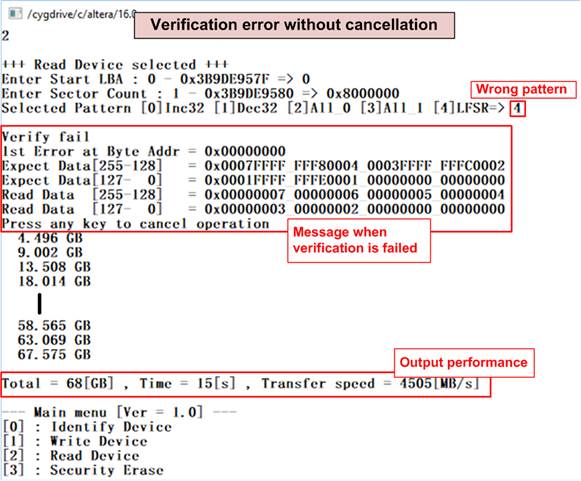
Figure 3‑6 Data verification is failed and wait until read complete

Figure 3‑7 Data verification is failed and press key to cancel operation
3.4 Security Erase
Select �3� to send Security Erase command to RAID0. Please confirm that all SATA devices support Security Erase feature by using Identify device menu. The estimated time of security erase operation is also displayed in Identify device menu.
After selecting the menu, confirmation message is displayed on NiosII command shell. User input �y� or �Y� to continue security erase operation or input other keys to cancel operation.
Number 0-9 is displayed NiosII command shell every second to show that system still run. After complete the operation, total time usage is displayed as a test result.
Figure 3‑9 shows the example when user inputs other keys to cancel the command.
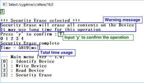
Figure 3‑8 Test result when running Security Erase command
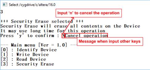
Figure 3‑9 Cancel Security Erase command
4 Revision History
|
Revision |
Date |
Description |
|
1.0 |
9-Mar-18 |
Initial version release |
|
1.1 |
15-May-19 |
Support Arria10 GX board |