RAID0 Design by using SATA Host-IP Manual
Rev1.2 22-Aug-23
1 Overview

Figure 1‑1 RAID0x4 Data Format
RAID0 system uses multiple storages to extend total storage capacity and increase write/read performance. Assumed that total number of device is N, RAID0 system capacity is equal to N times of one SATA device capacity. Write and read speed are almost equal to N times of the speed of one SATA device.
Data format of RAID0 is shown in Figure 1‑1. Data stream of the host side are split into a small stripe and transferred to one SATA device at a time. Stripe size is the unit size to store data in one SATA device before switching to other SATA devices.
In the reference design, four SATA devices are applied to run RAID0 system. Stripe size is equal to 512 byte (one sector). Four SATA devices connecting in the system should be same model to get the best performance and the best capacity. By using RAID0, the total capacity is equal to four times of SATA Device#0 capacity and the performance for write and read are almost four times. In our test system, Write speed of RAID0 is about 2000 MB/s and Read speed is about 2200 MB/s. (Performance from SATA Host-IP demo by using one SATA device are 510 MB/s for write command and 560 MB/s for read command).
User can modify RAID0 reference design to increase the numbers of SATA device in the system to achieve the better performance and bigger storage capacity.
Note: Comparing to RAID0 demo by using CPU in SATA-IP standard demo, the performance of Write command is much better because using SATA Host-IP can reduce the overhead time to process the packet.
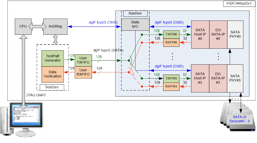
Figure 1‑2 RAID0x4 Demo System by using SATA Host-IP
RAID0x4 demo is modified from SATA Host-IP standard reference design. Please see more details of standard reference design from following link.
http://www.dgway.com/products/IP/SATA-IP/Altera/dg_satahostip_refdesign_alt_en.pdf
http://www.dgway.com/products/IP/SATA-IP/Altera/dg_satahostip_instruction_alt_en.pdf
To support RAID0 operation, Raid0x4 module is designed to be the interface block between user logic and four SATA Host-IPs. To support higher bandwidth, data bus size of RAID0 is increased to 128-bit (4 times of 32-bit which is SATA Host-IP bus size). To compatible with DG storage standard, the interface of Raid0x4 module is dgIF types. The user interface of Raid0x4 modules connects to Avl2Reg and TestGen (similar to SATA Host-IP standard demo), but data bus size is bigger.
Four sets of two FIFOs are connected between Raid0x4 and DG SATA Host-IP. They are used to be data buffer and also used to convert data bus size between 128-bit and 32-bit. For RAID0 operation, 128-bit data stream of UserFIFO is transferred to FIFO#0 � FIFO#3, selected by the logic inside Raid0x4 module. RAID0 logic switches the active SATA device after completing to transfer one stripe data (1 sector).
State machine of Raid0x4 is designed to receive and decode user input from CPU system such as the address and length through dgIF types (CMD) interface. The address and length of RAID0 are decoded to the value for each SATA Host-IP. After that, State machine sends the request with valid input to all SATA Host-IPs. Busy flag of all SATA Host-IPs is monitored until end of transfer.
User can modify 4-ch RAID0 reference design to support more SATA devices in the system. The numbers of SATA Host-IP, SATA-IP, SATA PHY, and FIFOs are increased following the numbers of SATA device. Also, the bus size between user logic and Raid0 module are extended to N x 32-bit to increase data bandwidth at user side. SATA device model in every channel should be the same.
To reduce clock resource utilization in SATA PHY of RAID0 system, there is one master SATA PHY in the system to generate clock and forward clock to other channels. The other channels are slave SATA PHY which receives clock from the master (no clock resource in Slave PHY). Only SATA-III device can support in the demo.
2 RAID0IP
Table 1 shows user interface of RAID0 module for both control and data interface. The interface is designed to dgIF typeS style. Comparing to SATA Host-IP, the status signals and data bus size are four times to support four channels.
Signal description of SATA Host-IP is described in SATA Host-IP datasheet.
http://www.dgway.com/products/IP/SATA-IP/Altera/dg_sata_host_ip_datasheet_alt_en.pdf
2.1 Port Description
Table 1 Signal Description of Raid block (only user interface)
|
Signal |
Dir |
Description |
|
User Interface |
||
|
RstB |
In |
Reset signal. Active low. Please use same reset signal as SATA Host-IP. |
|
Clk |
In |
User clock. Must use the same clock as SATA Host-IP. |
|
dgIF typeS |
||
|
UserCmd[1:0] |
In |
User Command. �00�: Identify device command, �01�: Security erase �10�: Write SATA device, �11�: Read SATA device. |
|
UserAddr[47:0] |
In |
Start address of write/read SATA device in sector unit (512 byte). |
|
UserLen[47:0] |
In |
Total transfer size in the request in sector unit (512 byte). Valid from 1 to (LBASize-UserAddr). |
|
UserReq |
In |
Request the new command. Can be asserted only when the IP is Idle (UserBusy=�0�). Asserted with valid value on UserCmd/UserAddr/UserLen signals. |
|
UserBusy |
Out |
IP Busy status. New request is not allowed if this signal is asserted to �1�. |
|
LBASize[47:0] |
Out |
Total capacity of RAID0 in sector unit (512 byte). Default value is 0. This value is equal to four times of LBASize value output from IP#0. |
|
UserError |
Out |
Error flag. Assert when UserErrorType is not equal to 0. The flag can be reset only by asserting RstB signal. |
|
UserErrorType[31:0] |
Out |
Error status which are mapped from status in each SATA Host-IP. [7:0] � Mapped from UserErrorType[7:0] of IP#0. [15:8] � Mapped from UserErrorType[7:0] of IP#1. [23:16] � Mapped from UserErrorType[7:0] of IP#2. [31:24] � Mapped from UserErrorType[7:0] of IP#3. |
|
UserFifoWrCnt[15:0] |
In |
Write data counter of User received FIFO. Used to check FIFO free space size. If total size is less than 16-bit, please fill �1� to upper bit. UserFifoWrEn can be asserted when UserFifoWrCnt[15:6] is not equal to all 1. |
|
UserFifoWrEn |
Out |
Write data valid of User received FIFO |
|
UserFifoWrData[127:0] |
Out |
Write data bus of User received FIFO. Synchronous to UserFifoWrEn. |
|
UserFifoRdCnt[15:0] |
In |
Read data counter of User transmit FIFO. Used to check data size in FIFO. If total FIFO size is less than 16-bit, please fill �0� to upper bit. UserFifoRdEn can be asserted when UserFifoRdCnt[15:5] is not equal to 0. |
|
UserFifoEmpty |
In |
FIFO empty flag of User transmit FIFO. This signal is unused in the design. |
|
UserFifoRdEn |
Out |
Read valid of User transmit FIFO |
|
UserFifoRdData[127:0] |
In |
Read data returned from User transmit FIFO. Valid in the next clock after UserFifoRdEn is asserted. |
|
Signal |
Dir |
Description |
|
Other Interface |
||
|
TestPin[0-3][31:0] |
Out |
Direct mapped from TestPin in each SATA Host-IP. [0]-IP#0, [1]-IP#1, [2]-IP#2, [3]-IP#3. |
|
TimeOutSet[31:0] |
Out |
Timeout value of all SATA Host-IPs. Time unit is following Clk frequency value. |
|
TrnLinkup[3:0] |
Out |
Linkup signal from trn_link_up in each SATA-IP. Bit[0]-IP#0, [1]-IP#1, [2]-IP#2, [3]-IP#3. |
|
IdenWrAddr[0-3][6:0] |
Out |
Direct mapped from IdenWrAddr in each SATA Host- IP. [0]-IP#0, [1]-IP#1, [2]-IP#2, [3]-IP#3. |
|
IdenWrEn[3:0] |
Out |
Direct mapped from IdenWrEn in each SATA Host- IP. [0]-IP#0, [1]-IP#1, [2]-IP#2, [3]-IP#3. |
|
IdenWrData[0-3][31:0] |
Out |
Direct mapped from IdenWrData in each SATA Host- IP. [0]-IP#0, [1]-IP#1, [2]-IP#2, [3]-IP#3. |
2.2 Timing Diagram
Timing diagram of RAID user interface and Identify device interface are similar to SATA Host-IP, so more details are described in IP datasheet. For RAID FIFO interface, the details are described as follows.
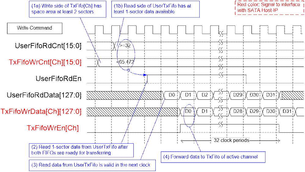
Figure 2‑1 RAID FIFO Timing Diagram of Write Command
When user sends write command to RAID system, data stream are forwarded from UserTxFifo to TxFifo[0]-[3]. Only one TxFifo is active to transfer one sector data. The active SATA channel is switched in the next sector transfer, following RAID0 behavior. Before forwarding data, UserFifoRdCnt and TxFifoWrCnt of active channel are monitored to confirm that at least 1 sector data is stored in UserTxFifo and at least 2-sector free space is available in TxFifo of active channel. UserFifoRdEn is asserted for 32 clock periods to transfer 512-byte data.
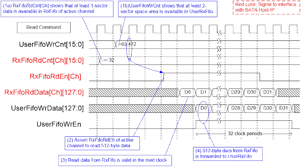
Figure 2‑2 RAID FIFO Timing Diagram of Read Command
When user sends read command to RAID system, data stream are forwarded from RxFifo[0]-[3] to UserRxFifo, as shown in Figure 2‑2. Similar to write command, only one RxFifo is active to transfer each 512-byte data. The active SATA channel is switched before transferring the next sector. Before forwarding data, UserFifoWrCnt and RxFifoRdCnt of active channel are monitored to confirm that at least 1 sector data is stored in RxFifo of active channel and at least 2-sector free space is available in UserRxFifo. UserFifoWrEn is asserted for 32 clock periods to transfer 512-byte data.
3 CPU
CPU system in RAID0 design is almost similar to SATA Host-IP standard demo. But register map for expected pattern and read pattern are extended from 32-bit to 128-bit, as shown in Table 2. The status signals are also extended to four channels.
Table 2 Register Map
|
Address |
Register Name |
Description |
|
Rd/Wr |
(Label in the �hsataraidtest.c�) |
|
|
BA+0x00 |
User Address (Low) Reg |
[31:0]: Input to be start sector address (UserAddr[31:0] of RAID0 following dgIF typeS) |
|
Wr |
(USRADRL_REG) |
|
|
BA+0x04 |
User Address (High) Reg |
[15:0]: Input to be start sector address (UserAddr[47:32] of RAID0 following dgIF typeS) |
|
Wr |
(USRADRH_REG) |
|
|
BA+0x08 |
User Length (Low) Reg |
[31:0]: Input to be transfer length in sector unit (UserLen[31:0] of RAID0 following dgIF typeS) |
|
Wr |
(USRLENL_REG) |
|
|
BA+0x0C |
User Length (High) Reg |
[15:0]: Input to be transfer length in sector unit (UserLen[47:32] of RAID0 following dgIF typeS) |
|
Wr |
(USRLENH_REG) |
|
|
BA+0x10 |
User Command Reg |
[1:0]: Input to be user command (UserCmd of RAID0 following dgIF typeS) �00�-Identify device, �01�-Secuity erase, �10�-Write SSD, �11�-Read SSD, When this register is written, the design generates command request to RAID0IP to start new command operation. |
|
Wr |
(USRCMD_REG) |
|
|
BA+0x14 |
Test Pattern Reg |
[2:0]: Test pattern select �000�-Increment, �001�-Decrement, �010�-All 0, �011�-All 1, �100�-LFSR |
|
Wr |
(PATTSEL_REG) |
|
|
BA+0x100 |
User Status Reg |
[0]: UserBusy of RAID0 following dgIF typeS (�0�: Idle, �1�: Busy) [1]: UserError of RAID0 following dgIF typeS (�0�: Normal, �1�: Error) [2]: Data verification fail (�0�: Normal, �1�: Error) [4:3]: SATA speed from IP �00�: No linkup, �11�: SATA Gen3, �01�/�10�: Not supported |
|
Rd |
(USRSTS_REG) |
|
|
BA+0x104 |
Total device size (Low) Reg |
[31:0]: Total capacity of RAID0 in sector unit (LBASize[31:0] of RAID0 following dgIF typeS) |
|
Rd |
(LBASIZEL_REG) |
|
|
BA+0x108 |
Total device size (High) Reg |
[15:0]: Total capacity of RAID0 in sector unit (LBASize[47:32] of RAID0 following dgIF typeS) |
|
Rd |
(LBASIZEH_REG) |
|
|
BA+0x10C |
User Error Type Reg |
[31:0]: User error status (UserErrorType[31:0] of RAID0 following dgIF typeS) |
|
Rd |
(USRERRTYPE_REG) |
|
|
BA+0x110 |
Test pin of SATA Host-IP#0 Reg |
[31:0]: Mapped to TestPin of SATA Host-IP#0 |
|
Rd |
(TESTPIN0_REG) |
|
|
BA+0x114 |
Test pin of SATA Host-IP#1 Reg |
[31:0]: Mapped to TestPin of SATA Host-IP#1 |
|
Rd |
(TESTPIN1_REG) |
|
|
BA+0x118 |
Test pin of SATA Host-IP#2 Reg |
[31:0]: Mapped to TestPin of SATA Host-IP#2 |
|
Rd |
(TESTPIN2_REG) |
|
|
BA+0x11C |
Test pin of SATA Host-IP#3 Reg |
[31:0]: Mapped to TestPin of SATA Host-IP#3 |
|
Rd |
(TESTPIN3_REG) |
|
|
BA+0x120 |
Data Failure Address (Low) Reg |
[31:0]: Latch value of failure address[31:0] in byte unit from read command |
|
Rd |
(RDFAILNOL_REG) |
|
|
BA+0x124 |
Data Failure Address (High) Reg |
[24:0]: Latch value of failure address [56:32] in byte unit from read command |
|
Rd |
(RDFAILNOH_REG) |
|
|
BA+0x130 |
Expected value Word0 Reg |
[31:0]: Latch value of expected data [31:0] from read command |
|
Rd |
(EXPPATW0_REG) |
|
|
BA+0x134 |
Expected value Word1 Reg |
[31:0]: Latch value of expected data [63:32] from read command |
|
Rd |
(EXPPATW1_REG) |
|
|
BA+0x138 |
Expected value Word2 Reg |
[31:0]: Latch value of expected data [95:64] from read command |
|
Rd |
(EXPPATW2_REG) |
|
|
BA+0x13C |
Expected value Word3 Reg |
[31:0]: Latch value of expected data [127:96] from read command |
|
Rd |
(EXPPATW3_REG) |
|
Address |
Register Name |
Description |
|
Rd/Wr |
(Label in the �hsataiptest.c�) |
|
|
BA+0x140 |
Read value Word0 Reg |
[31:0]: Latch value of read data [31:0] from read command |
|
Rd |
(RDPATW0_REG) |
|
|
BA+0x144 |
Read value Word1 Reg |
[31:0]: Latch value of read data [63:32] from read command |
|
Rd |
(RDPATW1_REG) |
|
|
BA+0x148 |
Read value Word2 Reg |
[31:0]: Latch value of read data [95:64] from read command |
|
Rd |
(RDPATW2_REG) |
|
|
BA+0x14C |
Read value Word3 Reg |
[31:0]: Latch value of read data [127:96] from read command |
|
Rd |
(RDPATW3_REG) |
|
|
BA+0x150 |
Current test byte (Low) Reg |
[31:0]: Current test data size of TestGen module in byte unit (bit[31:0]) |
|
Rd |
(CURTESTSIZEL_REG) |
|
|
BA+0x154 |
Current test byte (High) Reg |
[24:0]: Current test data size of TestGen module in byte unit (bit[56:32]) |
|
Rd |
(CURTESTSIZEH_REG) |
|
|
BA+0x2000 � 0x21FF |
Identify Device Command Data (IDENCTRL_REG) |
512-byte Identify Device Data from SATA Host-IP#0 |
|
BA+0x2200 � 0x23FF |
|
512-byte Identify Device Data from SATA Host-IP#1 |
|
BA+0x2400 � 0x25FF |
|
512-byte Identify Device Data from SATA Host-IP#2 |
|
BA+0x2600 � 0x27FF |
|
512-byte Identify Device Data from SATA Host-IP#3 |
4 TestGen
Comparing to SATA Host-IP single channel demo, data bus of test pattern is extended from 32-bit to 128-bit, as shown in Figure 4‑1.
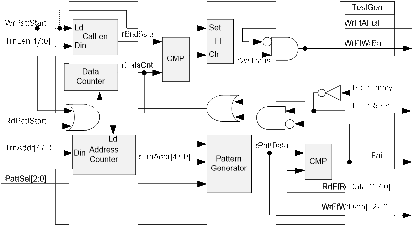
Figure 4‑1 Logic design in TestGen
5 Example Test Result
The example test result when running demo system by using 3x256 GB Samsung 850 Pro and 1x256 GB Samsung 860 Pro is shown in Figure 5‑1.
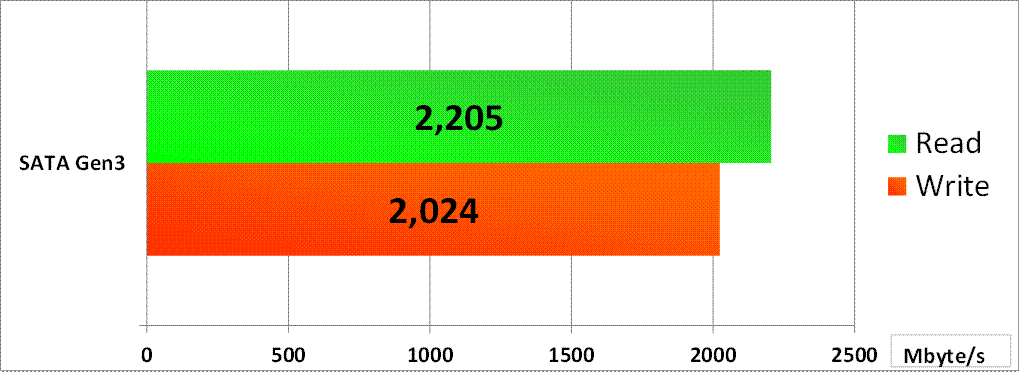
Figure 5‑1 Test Performance of RAID0x4 IP demo by using Samsung 850/860 Pro SSD
When running 4-ch RAID0 with 4 SATA Gen3 SSDs on Alaric board, write performance is about 2000 Mbyte/sec and read performance is about 2200 Mbyte/sec.
6 Revision History
|
Revision |
Date |
Description |
|
1.0 |
24-Nov-16 |
Initial version release |
|
1.1 |
24-Jan-17 |
Update signal to dgIF typeS |
|
1.2 |
15-Nov-17 |
Add LFSR pattern |
Copyright: 2016 Design Gateway Co,Ltd.