2.7 Xilinx Transceiver (PMA for 10GBASE-R)
4.1.3 Receive Data in Application Phase
4.1.4 Transmit Data in Application Phase
4.2.1 Check Hardware Access Permissions
This reference design demonstrates how TLS10GC-IP offloads encryption and decryption tasks when securely browsing via the Lynx web browser. With minimal modifications to the OpenSSL library and Lynx application on Ubuntu, users can achieve higher data transfer speeds while maintaining the same user experience.
1 System Overview
Figure 1 overview of the network communication structure on the client side
In secure communication, web browsers typically serve as clients communicating with web servers via the HTTPS protocol. An example of a network communication structure on the client side is shown as Figure 1(a). Lynx, a text-based web browser, functions as a user application that handles HTTP protocol, utilizes the OpenSSL library for managing TLS connections and uses socket for handling TCP connection and lower network layers.
The OpenSSL library handles TLS connection by managing TLS handshake, encrypting, and decrypting data packets exchanged during communication. However, this encryption and decryption process is resource-intensive, resulting in high CPU utilization. For compact edge devices such as KR260, CPU usage reaches 100% to handle these tasks and other necessary tasks that impacts the transfer speed of communication.
Design Gateway presents a reference design that uses high-performance security and network IP cores, i.e. TLS10GC-IP, TOE10GLL-IP and LL10GEMAC-IP, implemented in hardware logic of the KR260 to utilize the 10G ethernet port.
This document is divided into three sections based on system components as shown in Figure 1(b): Hardware, Kernel space, and User space.
· Hardware: User logic and IP cores for acceleration.
· Kernel space: Device drivers for interface between hardware and software in user space.
a) /dev/mem: Used for hardware register access
b) /dev/udmabuf: Used for handling memory
· User space: Modified Lynx and OpenSSL concept to support interfacing with the accelerator hardware.
Each system component's detailed functionality is described
in the following sections.
2 Hardware
Figure 2 TLS10GC-IP reference design block diagram
The hardware is connected to the CPU system via an AXI4-Lite interface for control path and AXI4 interface for data path.
For control path, the user-space software interacts with hardware registers via memory mapping. The memory mapping for hardware communication is separated into two regions: offset 0x000000-0x0000FF for TOE10GLL-IP and 0x800100-0x83FFFF for TLS10GS-IP. The AXI4-Lite interfaces are implemented using LAxi2TLS (for TLS10GS-IP) and LAxi2TOE (for TOE10GLL-IP), as shown in Figure 2.
For data path, The Xilinx AXI DMA controller is used to enable high-bandwidth direct memory access between DDR memory and hardware.
The user interface of the TLS10GC-IP connects to UserRegTLS within the LAxi2RegTLS module. UserRegTLS control data transmission and reception between the DMA Controller and TLS10GC-IP, as well as other user control operations for both components. UserRegTLS interfaces with the CPU through AsyncAXIReg using a register interface, with the CPU connecting to AsyncAXIReg via an AXI4-Lite interface.
For the DMA Controller, it is controlled by UserRegTLS via the AXI4-Lite interface. Data transmission occurs over a 128-bit AXI4 Stream interface (AXI4-ST) and transfer between hardware and the main memory in CPU occurs via the AXI4 interface.
The user interface of the TOE10GLL-IP connects to UserRegTOE within the LAxi2RegTOE module to control and monitor the operation of TOE10GLL-IP. UserRegTOE interfaces with the CPU through AsyncAXIReg using a register interface, while the CPU connects to AsyncAXIReg using an AXI4-Lite interface. The TOE10GLL-IP is also linked to a 10G Ethernet MAC controller (LL10GEMAC-IP) through a 32-bit AXI4 Stream interface (AXI4-ST). The LL10GEMAC-IP implements the Ethernet MAC layer and the PCS layer with low latency.
This design includes four clock domains:
· UserHClk: Used for CPU communication via the AXI4-Lite/AXI4 bus. It also be used for DMA Controller interfacing with user logic and serves as the high-frequency clock domain for TLS10GC-IP.
· UserLClk: Used as low frequency clock domain by TLS10GC-IP.
· TCPTxClk: Synchronized with the Tx EMAC interface and the Tx user data interface.
· TCPRxClk: Synchronized with the Rx EMAC interface and the Rx user data interface.
Details of each module are provided below.
2.1 LAxi2TLS
The LAxi2Reg module consists of AsyncAxiReg and UserRegTLS. AsyncAxiReg converts AXI4-Lite signals into a simple Register interface with a 32-bit data bus size, similar to AXI4-Lite standard. Additionally, it includes asynchronous logic to handle clock domain crossing between CpuClk and UserClk domains.
UserRegTLS contains the Register file for parameters, status signals and data path associated with TLS10GC-IP, including AXI DMA controller.
Additional details regarding AsyncAxiReg and UserRegTLS are provided below.
2.1.1 AsyncAxiReg
This module is designed to convert the signal interface of AXI4-Lite to be register interface. Also, it enables two clock domains to communicate.
The simple register interface is designed to be compatible with a single-port RAM interface for write transaction. For read transaction, the Register interface is slightly modified from the RAM interface by adding RdReq and RdValid signals to control read latency. Since the address of the Register interface is shared for both write and read transactions, the user cannot perform simultaneous write and read operations. The timing diagram for the Register interface is shown in Figure 3.
Figure 3 Register Interface Timing Diagram
1) To write register, the timing diagram is similar to that of a single-port RAM. The RegWrEn signal is set to 1b, along with a valid RegAddr (Register address in 32-bit units), RegWrData (write data for the register), and RegWrByteEn (write byte enable). The byte enable is four bits wide, where each bit indicates the validity of a specific byte within RegWrData. For example, if RegWrByteEn[0], [1], [2], and [3] are set to 1b, then RegWrData[7:0], [15:8], [23:16], and [31:24] are valid, respectively.
2) To read from a register, AsyncAxiReg sets the RegRdReq signal to 1b, along with a valid value for RegAddr. After the read request is processed, the 32-bit data is returned. The slave detects the RegRdReq being asserted to start the read transaction. During the read operation, the address value (RegAddr) remains unchanged until RegRdValid is set to 1b. Once valid, the address is used to select the returned data through multiple layers of multiplexers.
2.1.2 UserRegTLS
UserRegTLS is responsible for controlling and monitoring the TLS10GC-IP via address decoder, as well as managing data transfer between TLS10GC-IP and the AXI DMA controller via DMA control logic, as shown in Figure 4.
Figure 4 UserRegTLS block diagram
The address mapping is divided into two groups as follows.
0x0000 – 0x00FF: Control and status signals of TLS10GC-IP
0x0100 – 0x01FF: DMA control logic
To read register, multiple multiplexers are utilized to select data from each module, leading to increased real latency time due to the multiplexer. Therefore, RegRdValid is generated by RegRdReq through the assertion of two D Flip-flops.
Table 1 Register map Definition of TLS10GC-IP
|
Register Name |
Description |
|
|
TLS10GCIP control signal |
||
|
TLS_RSTB_REG |
Wr[0]: Reset signal active low (TLSRstB). |
|
|
0x00004 |
TLS_BUSY_REG |
Rd[1]: Busy status for
handshake operation (TLSHandshakeBusy). |
|
0x00008 |
TLS_ALERT_REG |
Rd[15:0]: Alert code from TLS10GC-IP (TLSAlertCode[15:0]). |
|
0x0000C |
TLS_TIMEOUT_REG |
Rd/Wr[15:0]: Timeout value for waiting returned packet (TLSTimeOut[15:0]). |
|
0x00010 |
TLS_MODESET_REG |
Wr[0]: Configure the mode of the TLS10GIP. ‘1’: Use full IP handshake. ‘0’: Use software handshake and IP only derives the key (rMode). When rMode is set, rModeSet is asserted to ‘1’ for the TLS10GIP. |
|
0x00014 |
TLS_PHASE_REG |
Wr[0]: Application transfer enable request (rAppTrnsEnReq). |
|
0x00018 |
CTS_IN_VALID_REG |
Wr[0]: Client Traffic Secret input valid (rCTSInValid). |
|
0x0001C |
STS_IN_VALID_REG |
Wr[0]: Server Traffic Secret input valid (rSTSInValid). |
|
0x00020-0x0004C |
CTS_IN_REG |
Rd/Wr[31:0]: Client Traffic Secret (CTS) |
|
0x00050-0x0007C |
STS_IN_REG |
Rd/Wr[31:0]: Server Traffic Secret (STS) |
|
0x00080 |
TX_SEQNUM_0_REG |
Rd/Wr[31:0]: 32-bit LSB start sequence number of Tx packet. |
|
0x00084 |
TX_SEQNUM_1_REG |
Rd/Wr[31:0]: 32-bit MSB start sequence number of Tx packet. |
|
0x00088 |
RX_SEQNUM_0_REG |
Rd/Wr[31:0]: 32-bit LSB start sequence number of Rx packet. |
|
0x0008C |
RX_SEQNUM_1_REG |
Rd/Wr[31:0]: 32-bit MSB start sequence number of Rx packet. |
|
DMA control logic |
||
|
0x00100 |
TLS_TX_RDPTR_REG |
Rd[13:0]: Read pointer to indicate the first byte position of TxData that IP will process (rTLSTxRdPtr). |
|
0x00104 |
TLS_TX_WRPTR_REG |
Rd/Wr[13:0]: Write pointer to indicate the position after the last TxData written (rTLSTxWrPtr). |
|
0x00108 |
TLS_RX_RDPTR_REG |
Rd/Wr[13:0]: Read pointer to indicate the first byte of RxData that user already to process (rTLSRxRdPtr). |
|
0x0010C |
TLS_RX_WRPTR_REG |
Rd[13:0]: Write pointer to indicate the position after the last RxData written (rTLSRxWrPtr). |
|
0x00110 |
APP_TX_RDPTR_REG |
Rd/Wr[19:0]: Read pointer to indicate the first byte position of UserTxData that DMA will process (rAppTxRdPtr). |
|
0x00114 |
APP_TX_WRPTR_REG |
Wr[19:0]: Write pointer to indicate the position after the user has written the last UserTxData (rAppTxUserWrPtr). Rd[19:0]: Write pointer to indicate the position of the last UserTxData that DMA will process (rAppTxWrPtr). |
|
0x00118 |
APP_RX_RDPTR_REG |
Rd/Wr[19:0]: Read pointer to indicate the first byte of UserRxData that the user has processed (rAppRxRdPtr). |
|
0x0011C |
APP_RX_WRPTR_REG |
Rd/Wr[19:0]: Write pointer to indicate the position after the last UserRxData written (rAppRxWrPtr). |
|
DMA Controller |
||
|
0x00130 |
SET_DMA_DST_H_ADDR |
Rd/Wr[31:0]: High address of the DMA destination (rS2MMDstBaseAddr[63:32]). |
|
0x00134 |
SET_DMA_DST_L_ADDR |
Rd/Wr[31:0]: Low address of the DMA destination (rS2MMDstBaseAddr[31:0]). |
|
0x00138 |
SET_DMA_SRC_H_ADDR |
Rd/Wr[31:0]: High address of the DMA source (rMM2sSrcBaseAddr[63:32]). |
|
0x0013C |
SET_DMA_SRC_L_ADDR |
Rd/Wr[31:0]: Low address of the DMA source (rMM2sSrcBaseAddr[31:0]). |
|
0x00140 |
DMA_STATUS_REG |
Wr[0]: DMA initialization (rDMAinit). Rd[0]: Receive transfer busy status (rRxTrnsBusy). Rd[1]: Transmit transfer busy status (rTxTrnsBusy). Rd[2]: DMA initialization status (rDMAinit). |
DMA control logic
This reference design implements an AXI DMA controller to transfer data between DDR memory and the hardware buffer in TLS10GC-IP. The DMA control logic in UserRegTLS manages data transactions by tracking the read and write pointers of both DDR memory and TLS10GC-IP, issuing commands to the AXI DMA controller as described below.
Transferring Tx data from DDR memory to TLS10GC-IP
To send data to hardware memory, the user writes the Tx data to DDR memory and updates the write pointer by writing to APP_TX_WRPTR_REG. Both DDR memory and the UserTxBuffer in TLS10GC-IP operate using a circular buffer mechanism. The available Tx data in DDR memory is determined by the write pointer (rAppTxWrPtr) and the read pointer (rAppTxRdPtr). The available free space in UserTxBuffer is determined by the write pointer (rTLSTxWrPtr) and the read pointer (rTLSTxRdPtr).
When Tx data is available in DDR memory and there is enough free space in UserTxBuffer, the DMA control logic sends a read command to the AXI DMA controller via the AXI4-Lite interface. The AXI4-Stream data received from the AXI DMA controller is converted to a write RAM interface and then written to the User Tx interface of TLS10GC-IP.
After completing the data transfer, rAppTxRdPtr is updated to the next read address and rTLSTxWrPtr is moved to notify TLS10GC-IP that Tx data is available for transmission.
Transferring Rx data from TLS10GC-IP to DDR memory
To receive data from hardware memory, the user reads the Rx data from DDR memory and updates the read pointer by writing to APP_RX_WRPTR_REG. Similar to Tx data, both DDR memory and UserRxBuffer in TLS10GC-IP follow a circular buffer mechanism. The available Rx data in UserRxBuffer is determined by the write pointer (rTLSRxWrPtr) and the read pointer (rTLSRxRdPtr). The available free space in DDR memory is determined by the write pointer (rAppRxWrPtr) and the read pointer (rAppRxRdPtr).
When Rx data is available in UserRxBuffer and there is sufficient free space in DDR memory, the DMA control logic sends a write command to the AXI DMA controller via the AXI4-Lite interface. The Rx data in UserRxBuffer is read via the read RAM interface, converted to AXI4-Stream, and transferred to the AXI DMA controller.
After completing the data transfer, rAppRxWrPtr is updated to the next write address and rTLSRxRdPtr is moved to notify TLS10GC-IP of the next address to read.
2.2 AXI DMA Controller
AXI DMA Controller can be generated by using Vivado IP catalog. The user uses the following settings as shown in Figure 5.
· Width of Buffer Length Register : 23
· Address Width : 64
· Enable Read Channel : Enable
· Enable Write Channel : Enable
Read Channel
· Number of Channel : 1
· Memory Map Data Width : 128
· Stream Data Width : 128
· Max Burst Size : 256
· Allow Unaligned Transfers : Enable
Write Channel
· Number of Channel : 1
· Memory Map Data Width : 128
· Stream Data Width : 128
· Max Burst Size : 256
· Allow Unaligned Transfers : Enable
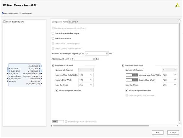
Figure 5 Example AXI DMA configuration page
The example of the AXI DMA Controller in the Ultrascale model is described in the following link.
https://www.xilinx.com/products/intellectual-property/axi_dma.html
2.3 TLS10GC-IP
TLS 1.3 Client 10Gbps IP Core (TLS10GC-IP) is designed to handle TLS 1.3 handshake for client, encrypt payload before sending over the network, and decrypt application data. User can write plain TxData to UserTxBuffer or read plain RxData from UserRxBuffer via read/write ram interface with a circular buffer concept. The control interface is used to configure the operation state, handshake parameters and monitors the operation status. The TCP interface utilizes a 32-bit AXI4 stream interface. More details are described in TLS10GC-IP datasheet.
https://dgway.com/products/IP/TLS-IP/TLS10GCIP-datasheet-xilinx-en/
2.4 LAxi2TOE
The LAxi2TOE module is connected to CPU through AXI4-Lite bus. LAxi2TOE consists of AsyncAxiReg and UserRegTOE. UserRegTOE is designed to write/read registers, control and check status of TOE10GLLIP corresponding with write register access or read register request from AsyncAxiReg module. Memory map inside UserRegTOE module is shown in Table 2.
Table 2 Register map Definition of TOE10GLLIP
|
Address offset |
Register Name |
Description |
|
0x00000 |
TOE_RST_INTREG |
Wr[0]: Mapped to RstB of TOE10GLL-IP |
|
0x00004 |
TOE_OPM_INTREG |
Wr[16]: Mapped to ARPICMPEn of TOE10GLL-IP Wr[1:0]: Mapped to DstMacMode of TOE10GLL-IP |
|
0x00008 |
TOE_SML_INTREG |
Wr[31:0]: Mapped to SrcMacAddr[31:0] of TOE10GLL-IP |
|
0x0000C |
TOE_SMH_INTREG |
Wr[15:0]: Mapped to SrcMacAddr[47:32] of TOE10GLL-IP |
|
0x00010 |
TOE_DMIL_INTREG |
Wr[31:0]: Mapped to DstMacAddr[31:0] of TOE10GLL-IP |
|
0x00014 |
TOE_DMIH_INTREG |
Wr[15:0]: Mapped to DstMacAddr[47:32] of TOE10GLL-IP |
|
0x00018 |
TOE_SIP_INTREG |
Wr[31:0]: Mapped to SrcIPAddr of TOE10GLL-IP |
|
0x0001C |
TOE_DIP_INTREG |
Wr[31:0]: Mapped to DstIPAddr of TOE10GLL-IP |
|
0x00020 |
TOE_TMO_INTREG |
Wr[31:0]: Mapped to TimeOutSet of TOE10GLL-IP |
|
0x00024 |
TOE_TIC_INTREG |
Wr[0]: Set ‘1’ to clear read value of TOE_STS_INTREG[2] |
|
0x00030 |
TOE_CMD_INTREG |
Wr[1:0]: Mapped to TCPCmd of TOE10GLL-IP. |
|
0x00034 |
TOE_SPN_INTREG |
Wr[15:0]: Mapped to TCPSrcPort[15:0] of TOE10GLL-IP |
|
0x00038 |
TOE_DPN_INTREG |
Wr[15:0]: Mapped to TCPDstPort[15:0] of TOE10GLL-IP |
|
0x00040 |
TOE_VER_INTREG |
Rd[31:0]: Mapped to IP version of TOE10GLL-IP |
|
0x00044 |
TOE_STS_INTREG |
Rd[20:16]: Mapped to IPState of TOE10GLL-IP Rd[2]: TOE10GLL-IP Interrupt. Asserted to ‘1’ when IPInt is asserted to ‘1’. This flag is cleared by TOE_TIC_INTREG. Rd[1]: Mapped to TCPConnOn of TOE10GLL-IP Rd[0]: Mapped to InitFinish of TOE10GLL-IP |
|
0x00048 |
TOE_INT_INTREG |
Rd[31:0]: Mapped to IntStatus of TOE10GLL-IP |
|
0x0004C |
TOE_DMOL_INTREG |
Rd[31:0]: Mapped to DstMacAddrOut[31:0] |
|
0x00050 |
TOE_DMOH_INTREG |
Rd[15:0]: Mapped to DstMacAddrOut[47:32] |
|
0x00060 |
EMAC_VER_INTREG |
Rd[31:0]: Mapped to IP version of DG LL10GEMAC-IP |
|
0x00064 |
EMAC_STS_INTREG |
Rd[0]: Mapped to Linkup of LL10GEMAC-IP |
|
0x00070 |
HW_ACCESS_REG |
Rd/Wr[0]: Mapped to rHwAccess flag |
2.5 TOE10GLL-IP
TOE10GLL-IP implements the TCP/IP stack and offload engine for the low latency solution. User interface has two signal groups, i.e., control signals and data signals. The IP can be configured to run in two modes, i.e., Cut-through mode for low-latency application and Simple mode for simple user interface. This reference design shows the usage in Simple mode. More details are described in datasheet.
https://dgway.com/products/IP/Lowlatency-IP/dg_toe10gllip_data_sheet_xilinx_en/
2.6 LL10GEMAC-IP
The IP core by Design Gateway implements low-latency EMAC and PCS logic for 10Gb Ethernet (BASE-R) standard. The user interface is 32-bit AXI4-stream bus. Please see more details from LL10GEMAC datasheet on our website.
https://dgway.com/products/IP/Lowlatency-IP/dg_ll10gemacip_data_sheet_xilinx_en/
2.7 Xilinx Transceiver (PMA for 10GBASE-R)
PMA IP core for 10Gb Ethernet (BASE-R) can be generated by using Vivado IP catalog. In FPGA Transceivers Wizard, the user uses the following settings.
· Transceiver configuration preset : GT-10GBASE-R
· Encoding/Decoding : Raw
· Transmitter Buffer : Bypass
· Receiver Buffer : Bypass
· User/Internal data width : 32
The example of Transceiver wizard in Ultrascale model is described in the following link.
https://www.xilinx.com/products/intellectual-property/ultrascale_transceivers_wizard.html
2.8 PMARstCtrl
When the buffer inside Xilinx Transceiver is bypassed, the user logic must control reset signal of Tx and Rx buffer. The module is designed by state machine to run following step.
(1) Assert Tx reset of the transceiver to ‘1’ for one cycle.
(2) Wait until Tx reset done, output from the transceiver, is asserted to ‘1’.
(3) Finish Tx reset sequence and de-assert Tx reset to allow the user logic beginning Tx operation.
(4) Assert Rx reset to the transceiver.
(5) Wait until Rx reset done is asserted to ‘1’.
(6) Finish Rx reset sequence and de-assert Rx reset to allow the user logic beginning Rx operation.
3 Kernel Space
This reference design uses the 5.15.0-1027-xilinx-zynqmp kernel image. To facilitate communication between hardware and user-space software while minimizing development time for additional device drivers, this reference design utilizes /dev/mem and /dev/udmabuf in the kernel space.
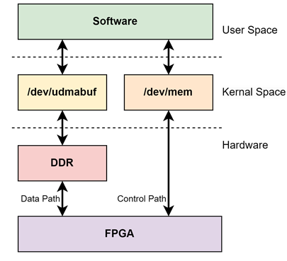
Figure 6 TLS10GC-IP reference design kernel space block diagram
3.1 /dev/mem
The /dev/mem provides direct access to the system’s physical memory and is commonly used for interacting with hardware registers in custom RTL designs implemented on the FPGA. In this reference design, /dev/mem is utilized for control path, allowing user-space applications to configure and monitor hardware components by mapping physical memory addresses to user space.
3.2 /dev/udmabuf
The /dev/udmabuf driver is a Linux device driver that allocates contiguous memory blocks as DMA buffers, making them accessible from user space. This reference design uses /dev/udmabuf for efficient data transfer between user-space applications and hardware accelerators.
The /dev/udmabuf driver supports two memory access modes:
· Non-cached mode: Direct memory access without CPU caching.
· Cached mode: CPU caching enabled, requiring manual cache management for consistency.
This reference design implements manual cache management with CPU caching enabled. When opening the /dev/udmabuf device file without setting the O_SYNC flag, CPU caching is enabled. To ensure data consistency, the driver provides mechanisms for users to manually invalidate and flush the cache via its device files. This feature is utilized in OpenSSL at the user-space level to maintain memory synchronization.
This reference design implements /dev/udmabuf v4.8.2.
For more details, please refer to:
· Official GitHub Repository: https://github.com/ikwzm/udmabuf/tree/v4.8.2
· Design Gateway Clone Repository: https://github.com/design-gateway/udmabuf
4 User Space
User space includes the OpenSSL library and the Lynx web browser. OpenSSL library is modified to work with TLS10GC-IP, offloading encryption and decryption tasks, while Lynx is modified to interface with TOE10GLL-IP for TCP connection. This section outlines the modifications made to OpenSSL and Lynx to enable CPU task offloading via DG’s security and network IP cores.
4.1 OpenSSL
OpenSSL is an open-source cryptographic library that implements TLS protocols for secure network communication. In this reference design, users can enable or disable TLS10GC-IP acceleration by setting the HW_ENABLE variable when launching Lynx from the command line:
· HW_ENABLE=1: TLS10GC-IP is enabled for encryption and decryption.
· HW_ENABLE≠1: Offloading is disabled, OpenSSL handles encryption and decryption in user space.
However, HW_ENABLE is only considered if ECONN is set to '10', indicating a 10G Ethernet interface is used.
The following subsections introduce modifications that enable OpenSSL to offload encryption and decryption tasks to TLS10GC-IP and How to build OpenSSL.
4.1.1 Set File Descriptor
OpenSSL processes transferred data through a layered BIO (Basic I/O) abstraction. The file descriptor serves as the input/output facility for TLS/SSL, typically representing a network socket. In the default OpenSSL implementation, socket BIO is automatically created to interface between the SSL structure and the file descriptor.
Since this reference design uses a hardware accelerator instead of a socket, a custom dgBIO (BIO_s_DG) structure is introduced to act as the interface between the SSL structure and the hardware. The modifications for integrating dgBIO are detailed below.
4.1.1.1 Define the dgBIO structure
The dgBIO structure is defined as BIO_BUF_DG in dgtls10gc.h. It interacts with hardware by accessing DDR memory via /dev/udmabuf, treating DDR memory as a circular buffer.
The members of the dgBIO structure are categorized into three groups: Transmit (Tx) side, Receive (Rx) side, and General parameters, as described below.
Transmit (Tx) side
· int tx_buffer_fd : File descriptor of the dgBIO buffer on the Tx side.
· char* tx_buffer : Pointer of the dgBIO buffer on the Tx side.
· int tx_read_pos : Next read position of the dgBIO buffer on the Tx side. Initial value: 0
· int tx_write_pos : Next write position of the dgBIO buffer on the Tx side. initial value: 0
· int tx_seq_num_H : 32-bit MSB of the next packet’s sequence number on the Tx side. initial value: 0
· int tx_seq_num_L : 32-bit LSB of the next packet’s sequence number on the Tx side. initial value: 0
Receive (Rx) side
· int rx_buffer_fd : File descriptor of the dgBIO buffer on the Rx side.
· char* rx_buffer : Pointer of the dgBIO buffer on the Rx side.
· int tx_read_pos : Next read position of the dgBIO buffer on the Rx side.Initial value: 0
· int rx_write_pos : Next write position of the dgBIO buffer on the Rx side. Initial value: 0
· int rx_ddr_wr_pos : Next write position hardware write data to DDR memory on Rx side. Initial value: 0
· int rx_seq_num_H : 32-bit MSB of the next packet’s sequence number on the Rx side. Initial value: 0
· int rx_seq_num_L : 32-bit LSB of the next packet’s sequence number on the Rx side. Initial value: 0
General parameters
· int max_size : Size of the dgBIO buffer on each side. Initial value: DG_BUFFER_SIZE.
· long pagesize : Kernel memory page size.
· void* hw_base_addr : Base address for register access.
4.1.1.2 Define dgBIO methods
The BIO_s_DG methods are implemented in crypto/bio/bss_dg.c. Each method is described below:
static int dg_bio_new(BIO *b)
This function creates a new dgBIO instance and initializes the BIO_s_DG members. The initialization process includes the following steps:
1. Map Memory Buffers
Map the contiguous memory blocks allocated as /dev/udmabuf0 and /dev/udmabuf1 to tx_buffer and rx_buffer, respectively.
2. Assign File Descriptors
Assign the file descriptors of /dev/udmabuf0 and /dev/udmabuf1 to tx_buffer_fd and rx_buffer_fd, allowing cache flushing and invalidation.
3. Set System Parameters
a. Set pagesize to the kernel memory page size.
b. Map hw_base_addr to the virtual base address of /dev/mem.
4. Initialize other BIO_s_DG members to their default values.
5. Obtain Physical Addresses
a. Get the source physical address from the phys_addr device file of /dev/udmabuf0.
b. Get the destination physical address from the phys_addr device file of /dev/udmabuf1.
6. Initialize DMA Control Parameters
a. Assert rDMAinit by writing 1 to DMA_STATUS_REG to begin DMA initialization.
b. Write the following registers with the respective physical addresses:
i. SET_DMA_SRC_H_ADDR, SET_DMA_SRC_L_ADDR with Source physical address.
ii. SET_DMA_DST_H_ADDR, SET_DMA_DST_L_ADDR with Destination physical address.
c. Initializes hardware read/write pointers for DDR memory:
i. APP_TX_RDPTR_REG, APP_TX_WRPTR_REG
ii. APP_RX_RDPTR_REG, APP_RX_WRPTR_REG
d. Complete DMA Initialization
7. Writes 0 to DMA_STATUS_REG to de-assert rDMAinit, completing the initialization process.
static int dg_bio_write(BIO *b, const char *data, int size)
This function attempts to write “size” bytes from “data” to dgBIO, “b”. It calls dgcpy_tx_cache() to write data to tx_buffer. It returns the number of bytes successfully written.
The dgcpy_tx_cache() function ensures efficient memory management by copying data to the buffer and flushing the cache to hardware. Its behavior is summarized in Figure 7 as a flowchart.
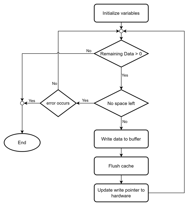
Figure 7 Modified dgcpy_tx_cache() function flow chart
Since this reference design operates with /dev/udmabuf in cache-enabled mode, the CPU cache must be flushed before updating the write pointer to hardware by calling sync_for_device() function. This function is defined in ssl/dgtls10gc.c. and issues an ioctl command to the u-dma-buf device file to flush the cache.
For more details about ioctl of u-dma-buf, please refer to
the GitHub repository:
https://github.com/ikwzm/udmabuf?tab=readme-ov-file#ioctl
static int dg_bio_read(BIO *b, char *data, int size)
This function attempts to “read” size bytes from dgBIO, “b”, and store the received data in “data”. It calls dgcpy_rx_cache() to retrieve data from rx_buffer. If no data is available, it sets the BIO_FLAGS_IN_EOF flag.
The dgcpy_rx_cache() manages memory efficiently by invalidating the cache and copying available data to data. If valid data is already in the buffer, it returns cached data. If no valid data is found, it checks available data in DDR and invalidates the cache accordingly. Its behavior is summarized in Figure 8 as a flowchart.
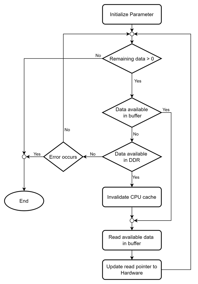
Figure 8 Modified dgcpy_rx_cache() function flow chart
The sync_for_cpu() function in ssl/dgtls10gc.c handles cache invalidation by issuing an ioctl command to u-dma-buf.
4.1.1.3 Assign dgBIO to SSL structure
When Lynx is executed with ECONN = 10, the SSL structure must use dgBIO as the interface for the file descriptor. To achieve this, the SSL_set_fd() function in ssl/ssl_lib.c is modified to create dgBIO and assign dgBIO to the SSL structure when ECONN=10 is detected.
4.1.2 Establish TLS Handshake
The SSL_connect() function in ssl/ssl_lib.c is responsible for establishing the TLS handshake. To enable the external handshake feature of TLS10GC-IP, SSL_connect() is as follows:
1. Register the necessary callback functions.
a. dg_ssl_info_callback(): This function sets the alert code detected by OpenSSL in hardware. It is declared in dgtls10gc.c and writes alerts to hardware by updating TLS_ALERT_REG.
b. dg_keylog_callback(): This function sets key materials in hardware. It is declared in dgtls10gc.c. When TLS key material is generated and identified as CLIENT_TRAFFIC_SECRET_0 or SERVER_TRAFFIC_SECRET_0, which are required by TLS10GC-IP to derive the application key for transfer data phase, these key materials are written to the hardware via CTS_IN_REG for CLIENT_TRAFFIC_SECRET_0 and STS_IN_REG for SERVER_TRAFFIC_SECRET_0.
2. Initialize the starting sequence number of Tx and Rx packets, which will be used by hardware.
3. Enable the data transfer flag to start offloading encryption/decryption process by TLS10GC-IP.
The modified SSL_connect() function is illustrated in Figure 9 as a flowchart.
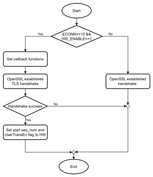
Figure 9 Modified SSL_connect() function flow chart
If HW_ENABLE variable is set to 1, the client's supported cipher suite in the ClientHello packet is restricted to TLS_AES_256_GCM_SHA384, which is the cipher suite supported by TLS10GC-IP. To enforce this, the ssl_cipher_list_to_bytes() function in ssl/statem/statem_clnt.c is modified to set only TLS_AES_256_GCM_SHA384 (ID: 0x1302) as the supported cipher suite.
To set the starting sequence number before enabling the UserTrnsEn flag of TLS10GC-IP, the tls13_cipher() function is modified to record the sequence number of the next packet in the dgBIO structure. This allows SSL_connect() to access the next sequence number and set it as the starting sequence number.
4.1.3 Receive Data in Application Phase
When offloading decryption tasks via TLS10GC-IP, the received application data from dgBIO is already decrypted. The SSL_read() function in ssl/ssl_lib.c can directly return the available data from rx_buffer to the user.
However, if TLS10GC-IP is disabled, the received data from dgBIO remains encrypted. In this case, OpenSSL must handle the decryption process following the standard flow.
4.1.4 Transmit Data in Application Phase
When offloading encryption task via TLS10GC-IP, the SSL_write() function in ssl/ssl_lib.c directly writes the plaintext application data from the user to dgBIO. The data is then transferred to hardware, where TLS10GC-IP encrypts it before sending through the network.
On the other hand, if TLS10GC-IP is disabled, OpenSSL encrypts the application data following its standard flow before writing it to dgBIO. In this case, the hardware simply bypasses the encrypted data and transmits it over the network.
4.1.5 Compile Custom OpenSSL
This reference design is based on OpenSSL version 3.3.1.
· Original OpenSSL Repository: https://github.com/openssl/openssl/tree/openssl-3.3.1
· Modified OpenSSL for TLS10GC-IP: https://github.com/design-gateway/openssl
To easily identify modifications, search for "[DGTLS10GC]" in the source code comments.
This reference design includes an example compilation and installation script (build.sh). Users can compile and install OpenSSL by running:
$ ./<OpenSSL source code>/build.sh
The build.sh script configures OpenSSL with the --prefix option, defining the installation directory. Users can modify this option to specify a custom output directory as needed.
4.2 Lynx
Lynx is a lightweight, customizable text-based browser that provides the core functionality of a standard web browser, making it well-suited for edge devices like the KR260. Similar to typical web browsers, Lynx acts as a client that communicates with web servers, establishes secure HTTPS connections, renders HTML, and processes HTTP protocol data.
In this reference design, Lynx is modified to support data transfer via both the 1G and 10G ethernet ports. Users can select the network interface by defining the ECONN variable when executing Lynx from the command line.
To transfer data through the 10G Ethernet interface. Lynx is modified to use TOE10GLL-IP instead of a standard socket, setting the necessary parameters for OpenSSL and hardware. The following subsections describe these modifications in detail.
4.2.1 Check Hardware Access Permissions
This reference design modifies Lynx to ensure that only one active TCP connection is allowed at a time when using TOE10GLL-IP. The HTLoadHTTP() function is responsible for managing HTTP requests and responses. Before calling HTDoConnect() to create a TCP connection, Lynx verifies hardware availability to prevent multiple processes from accessing TOE10GLL-IP simultaneously.
To manage hardware access, a hasAccess variable is introduced. When Lynx is executed with ECONN=10, it reads HW_ACCESS_REG to check the TOE10GLL-IP status. The rHwAccess flag within HW_ACCESS_REG determines hardware availability:
· If available, Lynx writes to HW_ACCESS_REG to set the rHwAccess flag, preventing other processes from using the hardware. The hasAccess variable is then set to TRUE.
· Before Lynx terminates, if hasAccess is TRUE, it clears rHwAccess by writing 0 to HW_ACCESS_REG.
The HTLoadHTTP() function in WWW/Library/Implementation/HTTP.c and the cleanup() and cleanup_sig() functions in src/LYClean.c are modified to manage these access controls.
4.2.2 Initial Parameters
Before opening a TCP connection via the 10G Ethernet interface, TOE10GLL-IP must be initialized with network parameters. This is handled by the init_param() function, located in WWW/Library/Implementation/dglynx10g.c, which retrieves network settings from configuration files. The parameters are:
· FPGA IP Address: Retrieved from /home/ubuntu/tool/lynx/etc/DG.cfg
· FPGA Port Number: Randomly selected from 0xC000 to 0xC0FF
· FPGA MAC Address: Retrieved from /home/ubuntu/tool/lynx/etc/DG.cfg
· Target IP Address: Resolved from the URL
· Target Port Number: Extracted from the URL
· Gateway IP Address: Retrieved from /home/ubuntu/tool/lynx/etc/DG.cfg
If TOE10GLL-IP cannot establish a connection using the target IP and port, init_param() will attempt to initialize it using the gateway IP address.
4.2.3 Open TCP Connection
The HTDoConnect() function in WWW/Library/implementation/HTTCP.c is responsible for establishing a network connection to a server. In the original flow, HTDoConnect() resolves the server’s hostname into an IP address, creates a network socket and attempts to establish a connection to the server using the resolved IP and specified port.
This reference design modifies HTDoConnect() to switch between the standard socket-based TCP mechanism and the TOE10GLL-IP core. When ECONN == 10, Lynx calls the read_conon() function to check the TOEConnOn status before initializing the TOE10GLL-IP core with network parameters. This prevents duplicate connections.
The read_conon() function, located in WWW/Library/Implementation/dglynx10g.c, reads the TOE_STS_INTREG register to check the current connection status of TOE10GLL-IP. Once initialization is complete, Lynx sends an open connection command to the TOE10GLL-IP core.
Since sockets are not used for 10G connections in this design, the file descriptor for the socket remains -1, indicating that a traditional socket is not in use.
4.2.4 Compile Custom Lynx
This reference design is based on Lynx-snapshots v2-9-2.
· Original Lynx Repository: https://github.com/ThomasDickey/lynx-snapshots/tree/v2-9-2
· Modified Lynx for TLS10GC-IP: https://github.com/design-gateway/lynx
To easily identify modifications, search for "[DGTLS10GC]" in the source code comments.
This reference design includes an example compilation and installation script (build.sh). Before compiling Lynx from source code, users must install the required libraries by running:
$ sudo apt install libncurses5
$ sudo apt install libncurses5-dev
$ sudo apt install libssl-dev
Once the dependencies are installed, users can compile and install Lynx by executing:
$ ./<lynx source code>/build.sh
The build.sh script configures Lynx with the --with-ssl option, pointing to the custom OpenSSL output directory, and the --prefix option, defining the installation directory. Users can modify these options to set a custom output directory as needed.
5 Revision History
|
Revision |
Date (D-M-Y) |
Description |
|
1.00 |
5-Mar-25 |
Initial version release |