TOE10G-IP with CPU reference design
Rev1.5 5-Jul-23
2.1 10/25Gb Ethernet PCS/PMA (10G BASE-R)
2.3 TenGMacIF (only when using Xilinx EMAC IP)
3.6 Function list in User application
4.1 �tcpdatatest� for half duplex test
4.2 �tcp_client_txrx_40G� for full duplex test
1 Introduction
TCP/IP is the core protocol of the Internet Protocol Suite for networking application. TCP/IP model has four layers, i.e., Application Layer, Transport Layer, Internet Layer and Network Access Layer. As shown in Figure 1‑1, five layers are displayed for simply matching with the hardware implementation on FPGA. Network Access Layer is split into Link and Physical Layer.
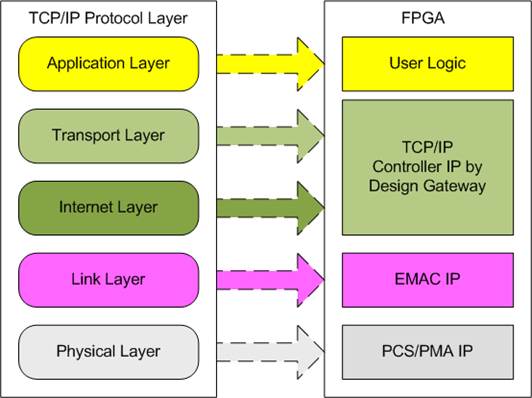
Figure 1‑1 TCP/IP Protocol Layer
TOE10G-IP implements Transport and Internet layer of TCP/IP Protocol for building Ethernet packet from the user data which is TCP payload data to EMAC. If TCP payload data size is larger than a packet size, TOE10G-IP splits the transmit data to multiple packets. Next, TCP payload data is appended by TCP/IP header. On the other hand, the received Ethernet packet from EMAC is extracted by TOE10G-IP. The header of the packet is verified. If the header is valid, TCP payload data is forwarded to the user logic. Otherwise, the packet is rejected.
The lower layer protocols are implemented by EMAC-IP and PCS/PMA-IP. PCS/PMA-IP is provided by Xilinx FPGA while EMAC-IP can be implemented by DG 10G25GEMAC-IP or Xilinx EMAC-IP.
The reference design provides the evaluation system which includes simple user logic to transfer data by using TOE10G-IP. TOE10G-IP supports to transfer data with PC or another TOE10G-IP run on another FPGA board. To run with PC, the test application is called on PC to send and verify TCP payload data via Ethernet connection at high-speed rate. Two test applications are specially designed, �tcpdatatest� for running half-duplex test (send or receive data test) and �tcp_client_txrx_40G� for running full-duplex test (send and receive data at the same time by one session).
To allow the user controlling the test parameters and the operation of TOE10G-IP demo via UART, the CPU system is included. It is easy for the user to set the test parameters and monitor the current status on UART console. The firmware on CPU is built by using bare-metal OS. More details of the demo are described as follows.
2 Hardware overview
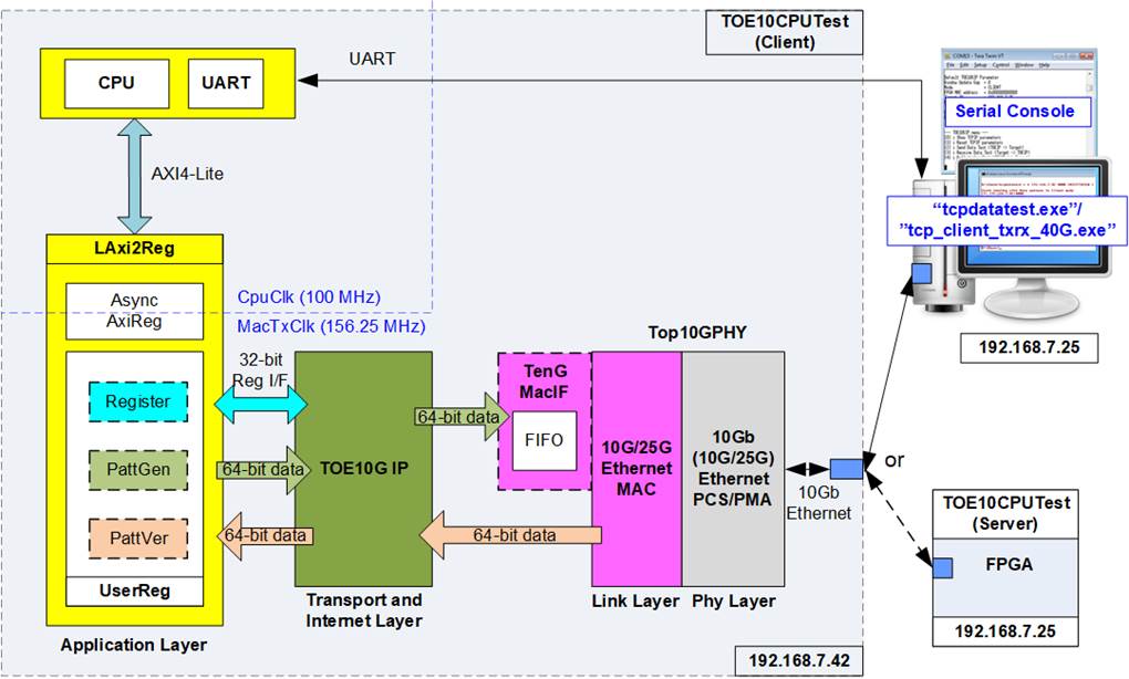
Figure 2‑1 Demo Block Diagram
In test environment, two devices are used for 10Gb Ethernet transferring. First device initializes in client mode and another device initializes in server mode. In the demo, the client device is TOE10G-IP on FPGA board while the server device can be TOE10G-IP on FPGA board or PC, as shown in Figure 2‑1. When using PC, the test applications (tcpdatatest and tcp_client_txrx_40G) must be run on PC to transfer data with TOE10G IP within FPGA.
In FPGA system, TOE10G-IP connects to 10G/25G Ethernet MAC and 10G/25G Ethernet PCS/PMA to implement all TCP/IP layers. User interface of TOE10G-IP connects to UserReg within AsyncAxiReg which consists of Register file for interfacing with Register interface, PattGen for sending test data via Tx FIFO interface, and PattVer for verifying test data via Rx FIFO interface. Register files of UserReg are controlled by CPU firmware through AXI4-Lite bus.
TenGMacIF is designed to be the data buffer between TOE10G-IP and Xilinx 10G EMAC-IP when Xilinx 10G EMAC-IP is not ready to receive the packet during one packet transmission. If using DG 10G25GEMAC-IP, TOE10G-IP can connect to EMAC directly without adding TenGMacIF.
Two clock domains are applied in the test design, i.e., CpuClk which is the independent clock for running the CPU system and MacTxClk which is the clock output from 10G/25G Ethernet PCS/PMA. So, AsyncAxiReg is designed to support asynchronous signals between CpuClk and MacTxClk. More details of each module inside the TOE10CPUTest are described as follows.
2.1 10/25Gb Ethernet PCS/PMA (10G BASE-R)
10/25Gb PCS/PMA implements physical layer of 10G Ethernet. It connects to the external hardware which is 10G BASE-R SFP+ module. The user interface is 64-bit XGMII interface running at 156.25 MHz which is designed to connect with 10G Ethernet MAC. This IP core is provided by Xilinx without the charge. More details of the core are described in the following link.
10G (10G/25G) Ethernet PCS/PMA (BASE-R)
https://www.xilinx.com/products/intellectual-property/10gbase-r.html
https://www.xilinx.com/products/intellectual-property/ef-di-25gemac.html
2.2 10G/25G Ethernet MAC
10G/25G EMAC connects between TOE10G-IP and 10G PCS/PMA module. The interface with TOE10G-IP is 64-bit AXI4 stream while the interface with 10G PCS/PMA module is 64-bit XGMII interface at 156.25 MHz.
When using DG 10G25GEMAC-IP, TOE10G IP can connect to EMAC IP directly, as shown in Figure 2‑2. More details about DG 10G25GEMAC-IP are described in the following link.
https://dgway.com/products/IP/GEMAC-IP/dg_10g25gemacip_data_sheet_xilinx.pdf
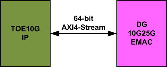
Figure 2‑2 TOE10G-IP connecting with DG 10G25GEMAC IP
When connecting with Xilinx 10G/25G EMAC-IP, the small buffer must be connected between TOE10G-IP and Xilinx 10G/25G EMAC-IP. So, TenGMacIF module is designed to be the interface module. More details of TenGMacIF are described in the next topic. The details of Xilinx EMAC are described in the following link.
https://www.xilinx.com/products/intellectual-property/do-di-10gemac.html
https://www.xilinx.com/products/intellectual-property/ef-di-25gemac.html
2.3 TenGMacIF (only when using Xilinx EMAC IP)

Figure 2‑3 TenGMacIF Block Diagram
Tx interface timing diagram of Xilinx 10G/25G EMAC and TOE10G-IP are different. TOE10G-IP needs to send data of one packet continuously, but Xilinx EMAC does not support this feature. Xilinx EMAC may de-assert ready signal to pause data receiving before end of the packet. TenGMacIF is designed to store transmitted data from TOE10G-IP when Xilinx 10G/25G EMAC is not ready to receive new data. According to real-board testing, tready output from Xilinx 10G EMAC is not de-asserted for long time per packet, so small FIFO which has 32-data depth is included to store the data during pausing time.
The operation of TenGMacIF is split into two sides, following the interface, i.e., Writing FIFO and Reading FIFO. Timing diagram for writing FIFO from TOE10G-IP is shown in Figure 2‑4 while timing diagram for reading FIFO and forwarding to Xilinx 10G EMAC is shown in Figure 2‑5.

Figure 2‑4 Write FIFO timing diagram of TenGMacIF
(1) Before asserting ToeMacReady to �1� for receiving the new data, two conditions must be met.
a) The logic checks if free space in FIFO is more than 16 by monitoring when FfDataCnt is less than 16.
Note: By real-board monitoring, it is found that Xilinx 10G/25G EMAC-IP de-asserts tx_axis_tready to �0� less than 16 cycles for each packet.
b) The previous packet is completely transferred more than two clock cycles by checking rToeMacReady[2]=�0�. rToeMacReady[2] is created by ToeMacReady with two clock cycle latency time. To pause the packet transmission, ToeMacReady is de-asserted to �0� to wait until EMAC and TenGMacIF is ready.
(2) During packet transmission, ToeMacValid from TOE10G-IP and ToeMacReady are asserted to �1� continuously until end of packet, so the packet is transferred without pausing time. In the next clock after ToeMacReady and ToeMacValid are asserted to �1�, rFfWrEn is asserted to �1� to store received data. FIFO data size is 73-bit for storing 64-bit data (ToeMacData), 8-bit of byte enable (ToeMacKeep), and last flag (ToeMacLast).
(3) When the last data is received (ToeMacLast=�1�), ToeMacReady is de-asserted to �0� for 3 clock cycles to be the gap size for each packet transmission.
Timing diagram to forward data from FIFO to Xilinx 10G EMAC is shown in Figure 2‑5.
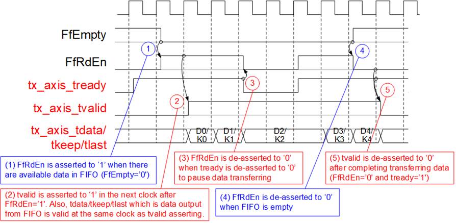
Figure 2‑5 Read FIFO timing diagram of TenGMacIF
(1) When the new packet is received from TOE10G-IP, FIFO empty (FfEmpty) is de-asserted to �0�. Since the packet from TOE10G-IP is transferred continuously, FIFO is not empty until a packet is completely transferred. The logic asserts read enable of FIFO (FfRdEn) to �1� for reading data from FIFO and forwarding data to Ethernet MAC.
(2) After reading data from FIFO, tx_axis_tvalid is asserted to �1� with the valid data for transferring to EMAC in the next cycle.
(3) When EMAC is not ready to receive data (tx_axis_tready=�0�), read enable must be de-asserted to �0� to pause data transmission.
(4) After the packet is completely transferred, the FIFO shows empty status (FfEmpty=�1�). At the same time, FfRdEn is de-asserted to �0� to stop data transmission.
(5) Next, tx_axis_tvalid is de-asserted to �0� to finish the packet transmission.
2.4 TOE10G-IP
TOE10G-IP implements TCP/IP stack and offload engine. User interface has two signal groups, i.e., control signals and data signals. Register interface is applied to set control registers and monitor status signals. Data signals are accessed by using FIFO interface. More details are described in datasheet.
http://www.dgway.com/products/IP/TOE10G-IP/dg_toe10gip_data_sheet_xilinx_en.pdf
2.5 CPU and Peripherals
32-bit AXI4-Lite is applied to be the bus interface for the CPU accessing the peripherals such as Timer and UART. To control and monitor the test system, the control and status signals are connected to register for CPU access as a peripheral through 32-bit AXI4-Lite bus. CPU assigns the different base address and the address range to each peripheral for accessing one peripheral at a time.
In the reference design, the CPU system is built with one additional peripheral to access the test logic. So, the hardware logic must be designed to support AXI4-Lite bus standard for supporting CPU writing and reading. LAxi2Reg module is designed to connect the CPU system as shown in Figure 2‑6.
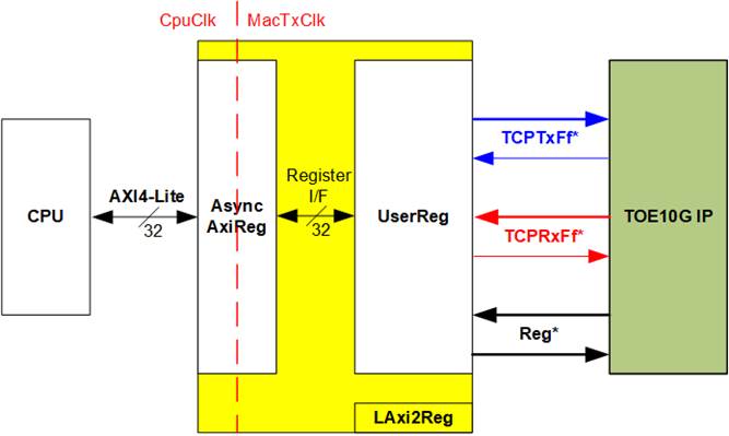
Figure 2‑6 LAxi2Reg block diagram
LAxi2Reg consists of AsyncAxiReg and UserReg. AsyncAxiReg is designed to convert the AXI4-Lite signals to be the simple register interface which has 32-bit data bus size (similar to AXI4-Lite data bus size). Additionally, AsyncAxiReg includes asynchronous logic to support clock domain crossing between CpuClk domain and MacTxClk domain.
UserReg includes the register file of the parameters and the status signals of test logics, including TOE10G-IP. Both data interface and control interface of TOE10G-IP are connected to UserReg. More details of AsyncAxiReg and UserReg are described as follows.
2.5.1 AsyncAxiReg
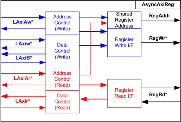
Figure 2‑7 AsyncAxiReg Interface
The signal on AXI4-Lite bus interface can be split into five groups, i.e., LAxiAw* (Write address channel), LAxiw* (Write data channel), LAxiB* (Write response channel), LAxiAr* (Read address channel), and LAxir* (Read data channel). More details to build custom logic for AXI4-Lite bus is described in following document.
According to AXI4-Lite standard, the write channel and the read channel are operated independently. Also, the control and data interface of each channel are run separately. So, the logic inside AsyncAxiReg to interface with AXI4-Lite bus is split into four groups, i.e., Write control logic, Write data logic, Read control logic, and Read data logic as shown in the left side of Figure 2‑7. Write control I/F and Write data I/F of AXI4-Lite bus are latched and transferred to be Write register interface with clock domain crossing registers. Similarly, Read control I/F of AXI4-Lite bus are latched and transferred to be Read register interface. While the returned data from Register Read I/F is transferred to AXI4-Lite bus by using clock domain crossing registers. In register interface, RegAddr is shared signal for write and read access, so it loads the address from LAxiAw for write access or LAxiAr for read access.
The simple register interface is compatible with single-port RAM interface for write transaction. The read transaction of the register interface is slightly modified from RAM interface by adding RdReq and RdValid signals for controlling read latency time. The address of register interface is shared for write and read transaction, so user cannot write and read the register at the same time. The timing diagram of the register interface is shown in Figure 2‑8.

Figure 2‑8 Register interface timing diagram
1) To write register, the timing diagram is similar to single-port RAM interface. RegWrEn is asserted to �1� with the valid signal of RegAddr (Register address in 32-bit unit), RegWrData (write data of the register), and RegWrByteEn (the write byte enable). Byte enable has four bits to be the byte data valid. Bit[0], [1], [2], and [3] are equal to �1� when RegWrData[7:0], [15:8], [23:16], and [31:24] are valid respectively.
2) To read register, AsyncAxiReg asserts RegRdReq to �1� with the valid value of RegAddr. 32-bit data must be returned after receiving the read request. The slave must monitor RegRdReq signal to start the read transaction. During read operation, the address value (RegAddr) does not change the value until RegRdValid is asserted to �1�. Therefore, the address can be used for selecting the returned data by using multiple layers of multiplexer.
3) The read data is returned on RegRdData bus by the slave with asserting RegRdValid to �1�. After that, AsyncAxiReg forwards the read value to LAxir* interface.
2.5.2 UserReg

Figure 2‑9 UserReg block diagram
The logic inside UserReg has three operations, i.e., Register, Pattern generator (PattGen), and Pattern verification (PattVer). Register block decodes the address requested from AsyncAxiReg and then selects the active register for write or read transaction. Pattern generator block is designed to send 64-bit test data to TOE10G-IP following FIFO interface standard. Pattern verification block is designed to read and verify 64-bit data from TOE10G-IP following FIFO interface standard. More details of each block are described as follows.
Register Block
The address range, mapped to UserReg, is split into two areas, i.e., TOE10G-IP register (0x0000-0x00FF) and UserReg register (0x1000-0x10FF).
Address decoder decodes the upper bit of RegAddr for selecting the active hardware. The register file inside UserReg is 32-bit bus size, so write byte enable (RegWrByteEn) is not used. To write hardware registers, the CPU must use 32-bit pointer to place 32-bit valid value on the write data bus.
To read register, multiplexer selects the read data within each address area. The lower bit of RegAddr is applied in each Register area to select the data. Next, the address decoder uses the upper bit to select the read data from each area for returning to CPU. Totally, the latency of read data is equal to one clock cycle, so RegRdValid is created by RegRdReq with asserting one D Flip-flop. More details of the address mapping within UserReg module are shown in Table 2‑1.
Table 2‑1 Register map Definition
|
Address |
Register Name |
Description |
|
Wr/Rd |
(Label in the �toe10gtest.c�) |
|
|
BA+0x0000 � BA+0x00FF: TOE10G-IP Register Area More details of each register are described in TOE10G-IP datasheet. |
||
|
BA+0x0000 |
TOE_RST_REG |
Mapped to RST register within TOE10G-IP |
|
BA+0x0004 |
TOE_CMD_REG |
Mapped to CMD register within TOE10G-IP |
|
BA+0x0008 |
TOE_SML_REG |
Mapped to SML register within TOE10G-IP |
|
BA+0x000C |
TOE_SMH_REG |
Mapped to SMH register within TOE10G-IP |
|
BA+0x0010 |
TOE_DIP_REG |
Mapped to DIP register within TOE10G-IP |
|
BA+0x0014 |
TOE_SIP_REG |
Mapped to SIP register within TOE10G-IP |
|
BA+0x0018 |
TOE_DPN_REG |
Mapped to DPN register within TOE10G-IP |
|
BA+0x001C |
TOE_SPN_REG |
Mapped to SPN register within TOE10G-IP |
|
BA+0x0020 |
TOE_TDL_REG |
Mapped to TDL register within TOE10G-IP |
|
BA+0x0024 |
TOE_TMO_REG |
Mapped to TMO register within TOE10G-IP |
|
BA+0x0028 |
TOE_PKL_REG |
Mapped to PKL register within TOE10G-IP |
|
BA+0x002C |
TOE_PSH_REG |
Mapped to PSH register within TOE10G-IP |
|
BA+0x0030 |
TOE_WIN_REG |
Mapped to WIN register within TOE10G-IP |
|
BA+0x0034 |
TOE_ETL_REG |
Mapped to ETL register within TOE10G-IP |
|
BA+0x0038 |
TOE_SRV_REG |
Mapped to SRV register within TOE10G-IP |
|
BA+0x003C |
TOE_VER_REG |
Mapped to VER register within TOE10G-IP |
|
BA+0x1000 � BA+0x10FF: UserReg control/status |
||
|
BA+0x1000 |
Total transmit length |
Wr [31:0] � Total transmit size in Qword unit (64-bit). Valid from 1-0xFFFFFFFF. Rd [31:0] � Current transmit size in Qword unit (64-bit). The value is cleared to 0 when USER_CMD_REG is written by user. |
|
Wr/Rd |
(USER_TXLEN_REG) |
|
|
BA+0x1004 |
User Command |
Wr [0] � Start Transmitting. Set �0� to start transmitting. [1] � Data Verification enable (�0�: Disable data verification, �1�: Enable data verification) Rd [0] � Tx Busy (�0�: Idle, �1�: Tx module is busy) [1] � Data verification error (�0�: Normal, �1�: Error) This bit is auto-cleared when user starts new operation or reset. [2] � Mapped to ConnOn signal of TOE10G-IP |
|
Wr/Rd |
(USER_CMD_REG) |
|
|
BA+0x1008 |
User Reset |
Wr [0] � Reset signal. Set �1� to reset the logic. This bit is auto-cleared to �0�. [8] � Set �1� to clear TimerInt latched value Rd [8] � Latched value of TimerInt output from IP (�0�: Normal, �1�: TimerInt=�1� is detected) This flag can be cleared by system reset condition or setting USER_RST_REG[8]=�1�. [16] � Ethernet linkup status from Ethernet MAC (�0�: Not linkup, �1�: Linkup) |
|
Wr/Rd |
(USER_RST_REG) |
|
|
BA+0x100C |
FIFO status |
Rd [2:0] - Mapped to TCPRxFfLastRdCnt signal of TOE10G-IP [15:3] - Mapped to TCPRxFfRdCnt signal of TOE10G-IP [24] - Mapped to TCPTxFfFull signal of TOE10G-IP |
|
Rd |
(USER_FFSTS_REG) |
|
|
BA+0x1010 |
Total receive length |
Rd [31:0] � Current receive size in Qword unit (64-bit). The value is cleared to 0 when USER_CMD_REG is written by user. |
|
Rd |
(USER_RXLEN_REG) |
|
|
BA+0x1080 |
EMAC IP version |
Rd[31:0] � Mapped to IPVersion output from DG 10G25GEMAC-IP when the system integrates DG 10G25GEMAC-IP. |
|
Rd |
(EMAC_VER_REG) |
|
Pattern Generator
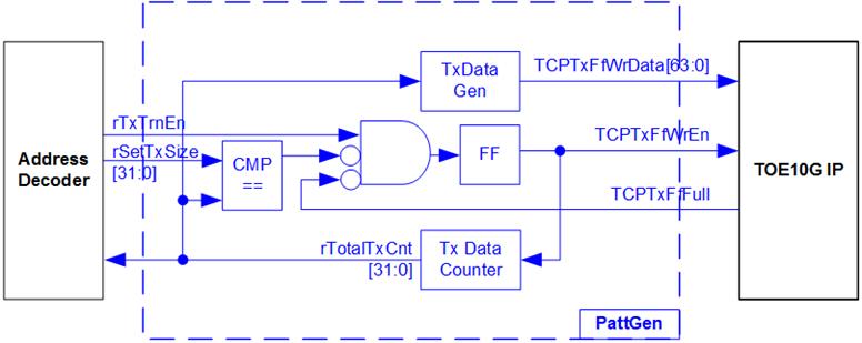
Figure 2‑10 PattGen block
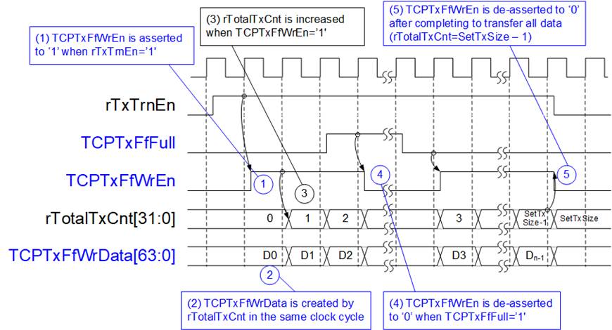
Figure 2‑11 PattGen Timing diagram
Figure 2‑10 shows the details of PattGen which generates test data to TOE10G-IP. Timing diagram to show the relation of each logic is displayed in Figure 2‑11.
To start PattGen operation, the user sets USER_CMD_REG[0]=�0� and then rTxTrnEn is asserted to �1�. When rTxTrnEn is �1�, TCPTxFfWrEn is controlled by TCPTxFfFull. TCPTxFfWrEn is de-asserted to �0� when TCPTxFfFull is �1�. rTotalTxCnt is the data counter to check total amount of transmitted data to TOE10G-IP. Also, rTotalTxCnt is used to generate 32-bit incremental data for TCPTxFfWrData signal. After all data is transferred completely (Total amount of data is equal to rSetTxSize-1), rTxTrnEn is de-asserted to �0�.
Pattern Verification
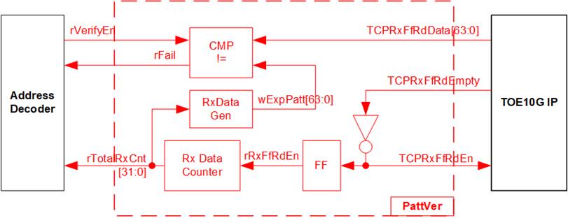
Figure 2‑12 PattVer block
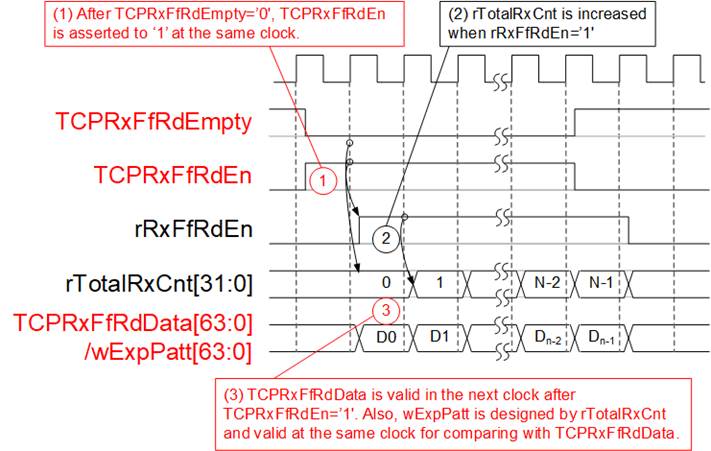
Figure 2‑13 PattVer Timing diagram
Figure 2‑12 shows the details of PattVer logic for reading the data from TOE100G-IP with or without data verification, controlled by rVerifyEn flag which is set by the user. Timing diagram of the logic is displayed in Figure 2‑13.
When rVerifyEn is set to �1�, data comparison is enabled to compare read data (TCPRxFfRdData) with the expected pattern (wExpPatt). If data verification is failed, rFail is asserted to �1�. TCPRxFfRdEn is designed by using NOT logic of TCPRxFfRdEmpty. TCPRxFfRdData is valid for data comparison in the next clock. rRxFfRdEn, one clock latency of TCPRxFfRdEn, is applied to be counter enable of rTotalRxCnt, counting total amount of received data. rTotalRxCnt is used to generate wExpPatt, so wExpPatt is valid at the same time as TCPRxFfRdData valid.
3 CPU Firmware on FPGA
· When testing by FPGA and PC, it is recommended to initialize TOE10G-IP in Client mode. After PC receives ARP request from TOE10G-IP, PC returns ARP reply. It is not simple to force PC sending ARP request to complete FPGA initialization in Server mode.
· When testing by two FPGAs, the initialization mode on two FPGAs must be different, server mode and client mode.
The software has two default parameters for each operation mode. After receiving the mode from the user, the default parameters in the selected mode are displayed on the console. The user can select to complete the initialization by using default parameters or updated parameters. The example when the system is initialized in Client mode by using default parameters is shown in Figure 3‑1.

Figure 3‑1 System initialization in Client mode by using default parameters
There are four steps to complete initialization process as follows.
1) CPU receives the initialization mode and then displays default parameters of the selected mode mode on the console.
2) User inputs �x� to complete initialization process by using default parameters. Other keys are set for changing some parameters. More details for changing some parameters are described in Reset IP menu (topic 3.2).
3) CPU waits until TOE10G-IP finishes initialization process (TOE_CMD_REG[0]=�0�).
4) Main menu is displayed. There are five test operations for user selection. More details of each menu are described as follows.
3.1 Show parameters
This menu is used to show current parameters of TOE10G-IP, i.e., the initialization mode, Windows update threshold, Reverse packet enable, source MAC address, destination IP address, source IP address, destination port and source port. The sequence of display parameters is as follows.
1) Read all network parameters from each variable in firmware.
2) Print out each variable.
3.2 Reset IP
This menu is used to change TOE10G-IP parameters such as IP address and source port number. After setting updated parameter to TOE10G-IP register, the CPU resets the IP to re-initialize by using new parameters. Finally, the CPU monitors busy flag to wait until the initialization is completed. The sequence to reset IP is as follows.
1) Display current parameter value on the console.
2) Receive initialization mode from user and confirm that input is valid. If initialization mode is changed, the latest parameter set of new mode is displayed on the console.
4) Reset PattGen and PattVer logic by sending reset to user logic (USER_RST_REG[0]=�1�).
5) Force reset to IP by setting TOE_RST_REG[0]=�1�.
6) Set all parameters to TOE10G-IP register such as TOE_SML_REG and TOE_DIP_REG.
7) De-assert IP reset by setting TOE_RESET_REG[0]=�0�. After that, TOE100G-IP starts the initialization process.
8) Monitor IP busy flag (TOE_CMD_REG[0]) until the initialization process is completed (busy flag is de-asserted to �0�).
3.3 Send data test
Three user inputs are received to set total transmit length, packet size, and connection mode (active open for client operation or passive open for server operation). The operation is cancelled if some inputs are invalid. During the test, 32-bit incremental data is generated from the logic and sent to the target (PC or FPGA). The received data is verified by the target (PC or FPGA). After all data are transferred completely, the operation is exit. More details of this menu are described as follows.
1) Receive transfer size, packet size, and connection mode from user and verify that all inputs are valid.
2) Set UserReg registers, i.e., transfer size (USER_TXLEN_REG), reset flag to clear initial value of test pattern (USER_RST_REG[0]=�1�), and command register to start data pattern generator (USER_CMD_REG=0). After that, test pattern generator in UserReg starts sending data to TOE10G-IP.
3) Display recommended parameters of test application on PC by reading current parameters in the system.
4) Open connection following connection mode value.
a) For active open, CPU sets TOE_CMD_REG=2 (Open port) and monitors ConnOn status (USER_CMD_REG[2]) until it is equal to �1�.
b) For passive open, CPU waits until connection is opened by PC or FPGA. ConnOn status (USER_CMD_REG[2]) is monitored until it is equal to �1�.
5) Set packet size to TOE10G-IP register (TOE_PKL_REG) and calculate total number of loops from total transfer size. Maximum transfer size of each loop is 4 GB. The operation of each loop is as follows.
i) Set transfer size of this loop to TOE10G-IP register (TOE_TDL_REG). Transfer size is fixed to 4 GB except the last loop which is equal to the remaining size.
ii) Set send command to TOE10G-IP register (TOE_CMD_REG=0).
iii) Wait until operation is completed by monitoring busy flag (TOE_CMD_REG[0]=�0�). During monitoring busy flag, CPU reads current amount of transmitted data from user logic (USER_TXLEN_REG) and displays the results on the console every second.
6) Set close connection command to TOE10G-IP register (TOE_CMD_REG=3).
7) Calculate performance and show test result on the console.
3.4 Receive data test
User sets total amount of received data, data verification mode (enable or disable), and connection mode (active open for client operation or passive open for server operation). The operation is cancelled if some inputs are invalid. During the test, 32-bit incremental data is generated to verify the received data from PC/FPGA when data verification mode is enabled. The sequence of this test is as follows.
1) Receive total transfer size, data verification mode, and connection mode from user input. Verify that all inputs are valid.
2) Set UserReg registers, i.e., reset flag to clear the initial value of test pattern (USER_RST_REG[0]=�1�) and data verification mode (USER_CMD_REG[1]=�0� or �1�).
3) Display recommended parameter (similar to Step 3 of Send data test).
4) Open connection following connection mode (similar to Step 4 of Send data test).
5) Wait until connection is closed by PC or FPGA. Connon status (USER_CMD_REG[2]) is monitored until it is equal to �0�. During monitoring Connon, CPU reads current amount of received data from user logic (USER_RXLEN_REG) and displays the results on the console every second.
6) Wait until all data are read by user logic completely by checking FIFO status (USER_FFSTS_REG[15:0]=0).
7) Compare receive length of user logic (USER_RXLEN_REG) with the set value from user. If all data is completely received, CPU checks verification result by reading USER_CMD_REG[1] (�0�: normal, �1�: error). If some errors are detected, the error message is displayed.
8) Calculate performance and show test result on the console.
3.5 Full duplex test
This menu is designed to run full duplex test by transferring data between FPGA and PC/FPGA in both directions by using the same port number at the same time. Four inputs are received from user, i.e., total data size for both transfer directions, packet size for FPGA sending logic, data verification mode for FPGA receiving logic, and connection mode (active open/close for client operation or passive open/close for server operation).
When running the test by using PC, the transfer size set on FPGA must be matched to the size set on test application (tcp_client_txrx_40G). Connection mode on FPGA when running with PC must be set to passive (server operation).
The test runs in forever loop until the user cancels operation. The operation can be cancelled by entering any keys on FPGA console and then entering Ctrl+C on PC console. The sequence of this test is as follows.
1) Receive total data size, packet size, data verification mode, and connection mode from the user and verify that all inputs are valid.
2) Display the recommended parameters of test application run on PC from the current system parameters.
3) Set UserReg registers, i.e., transfer size (USER_TXLEN_REG), reset flag to clear the initial value of test pattern (USER_RST_REG[0]=�1�), and command register to start data pattern generator with data verification mode (USER_CMD_REG=1 or 3).
4) Open connection following the connection mode value (similar to Step 4 of Send data test).
5) Set packet size to TOE10G-IP registers (TOE_PKL_REG=user input) and calculate total transfer size in each loop. Maximum size of one loop is 4 GB. The operation of each loop is as follows.
i) Set transfer size of this loop to TOE_TDL_REG. Transfer size is fixed to maximum size (4GB) which is also aligned to packet size, except the last loop. The transfer size of the last loop is equal to the remaining size.
ii) Set send command to TOE10G-IP register (TOE_CMD_REG=0).
iii) Wait until send command is completed by monitoring busy flag (TOE_CMD_REG[0] =�0�). During monitoring busy flag, CPU reads current amount of transmitted data and received data from user logic (USER_TXLEN_REG and USER_RXLEN_REG) and then displays the results on the console every second.
6) Close connection following connection mode value.
a. For active close, CPU waits until total amount of received data is equal to the set value from user. Then, set USER_CMD_REG=3 to close connection. Next, CPU waits until connection is closed by monitoring ConnOn (USER_CMD_REG[2]=�0�).
b. For passive close, CPU waits until the connection is closed from FPGA/PC by monitoring ConnOn (USER_CMD_REG[2]=�0�).
7) Check the result and the error (similar to Step 6-7 of Receive data test).
8) Calculate performance and show the test result on the console. Go back to step 3 to repeat the test in forever loop.
3.6 Function list in User application
This topic describes the function list to run TOE10G-IP operation.
|
void exec_port(unsigned int port_ctl, unsigned int mode_active) |
|
|
Parameters |
port_ctl: 1-Open port, 0-Close port mode_active: 1-Active open/close, 0-Passive open/close |
|
Return value |
None |
|
Description |
For active mode, write TOE_CMD_REG to open or close connection. After that, call read_conon function to monitor connection status until it changes from ON to OFF or OFF to ON, depending on port_ctl mode. |
|
void init_param(void) |
|
|
Parameters |
None |
|
Return value |
None |
|
Description |
Ask the user if the parameters are updated. After that, set the parameters to TOE10G-IP registers from global parameters. After reset is de-asserted, it waits until TOE10G-IP busy flag is de-asserted to �0�. |
|
int input_param(void) |
|
|
Parameters |
None |
|
Return value |
0: Valid input, -1: Invalid input |
|
Description |
Receive network parameters from user, i.e., Mode, Window threshold, FPGA MAC address, FPGA IP address, FPGA port number, Target IP address and Target port number. If the input is valid, the parameter is updated. Otherwise, the value does not change. After receiving all parameters, the current value of each parameter is displayed. |
|
Unsigned int read_conon(void) |
|
|
Parameters |
None |
|
Return value |
0: Connection is OFF, 1: Connection is ON. |
|
Description |
Read value from USER_CMD_CONNON register and return only bit2 value to show connection status. |
|
void show_cursize(void) |
|
|
Parameters |
None |
|
Return value |
None |
|
Description |
Read USER_TXLEN_REG and USER_RXLEN_REG and then display the current amount of transmitted data and receive data in Byte, KByte, or MByte unit |
|
void show_param(void) |
|
|
Parameters |
None |
|
Return value |
None |
|
Description |
Display the current value of the network parameters set to TOE10G-IP such as IP address, MAC address and port number. |
|
void show_result(void) |
|
|
Parameters |
None |
|
Return value |
None |
|
Description |
Read USER_TXLEN_REG and USER_RXLEN_REG to display total amount of transmitted data and received data. Next, read the global parameters (timer_val_end and timer_val_start) and calculate total time usage to display in usec, msec, or sec unit. Finally, transfer performance is calculated and displayed in MB/s unit. |
|
int toe_recv_test(void) |
|
|
Parameters |
None |
|
Return value |
0: The operation is successful -1: Receive invalid input or error is found |
|
Description |
Run Receive data test following description in topic 3.4 |
|
int toe_send_test(void) |
|
|
Parameters |
None |
|
Return value |
0: The operation is successful -1: Receive invalid input or error is found |
|
Description |
Run Send data test following description in topic 3.3 |
|
int toe_txrx_test(void) |
|
|
Parameters |
None |
|
Return value |
0: The operation is successful -1: Receive invalid input or error is found |
|
Description |
Run Full duplex test following described in topic 3.5 |
|
void wait_ethlink(void) |
|
|
Parameters |
None |
|
Return value |
None |
|
Description |
Read USER_RST_REG[16] and wait until ethernet connection is linked up |
4 Test Software on PC
4.1 �tcpdatatest� for half duplex test
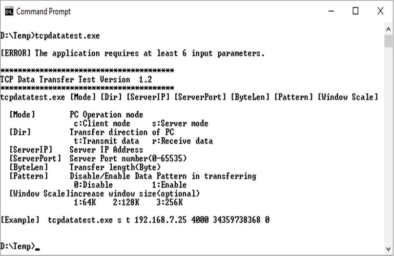
Figure 4‑1 �tcpdatatest� application usage
�tcpdatatest� is designed to run on PC for sending or receiving TCP data via Ethernet as Server and Client mode. PC of this demo runs in Client mode. User sets parameter to select transfer direction and the mode. Six parameters are required as follows.
1) Mode: c �PC runs in Client mode and FPGA runs in Server mode
2) Dir: t � transmit mode (PC sends data to FPGA)
r � receive mode (PC receives data from FPGA)
3) ServerIP: IP address of FPGA when PC runs in Client mode (default is 192.168.7.42)
4) ServerPort: Port number of FPGA when PC runs in Client mode (default is 4000)
5) ByteLen: Total transfer size in byte unit. This input is used in transmit mode only and ignored in receive mode. In receive mode, the application is closed when the connection is terminated. In transmit mode, ByteLen must be equal to the total transfer size on FPGA, set in receive data test menu.
6) Pattern:
0 � Generate dummy data in transmit mode or disable data verification in receive mode.
1 � Generate incremental data in transmit mode or enable data verification in receive mode.
Note: Window Scale: Optional parameter which is not used in the demo.
Transmit data mode
Following sequence is the sequence when test application runs in transmit mode.
1) Get parameters from the user and verify that the input is valid.
2) Create the socket and set socket options.
3) Create the new connection by using server IP address and server port number.
4) Allocate 1 MB memory to be send buffer.
5) Skip this step if the dummy pattern is selected. Otherwise, generate the incremental test pattern to send buffer when the test pattern is enabled.
6) Send data out and read total sent data from the function.
7) Calculate remaining transfer size.
8) Print total transfer size every second.
9) Repeat step 5) � 8) until the remaining transfer size is 0.
10) Calculate total performance and print the result on the console.
11) Close the socket and free the memory.
Receive data mode
Following sequence is the sequence when test application runs in receive mode.
1) Follow the step 1) � 3) of Transmit data mode.
2) Allocate memory to be receive buffer.
3) Read data from the receive buffer and increase total amount of received data.
4) This step is skipped if data verification is disabled. Otherwise, received data is verified by the incremental pattern. Error message is printed out when data is not correct.
5) Print total amount of received data every second.
6) Repeat step 3) � 5) until the connection is closed.
7) Calculate total performance and print the result on the console.
8) Close socket and free the memory.
4.2 �tcp_client_txrx_40G� for full duplex test

Figure 4‑2 �tcp_client_txrx_40G� application usage
�tcp_client_txrx_40G� application is designed to run on PC for sending and receiving TCP data through Ethernet by using the same port number at the same time. The application is run in Client mode, so user needs to input server parameters (the network parameters of TOE10G-IP). As shown in Figure 4‑2, there are four parameters to run the application, described as follows.
1) ServerIP : IP address of FPGA
2) ServerPort : Port number of FPGA
3) ByteLen : Total transfer size in byte unit. This is total amount of transmitted data and received data.
4) Verification :
0 � Generate dummy data for sending function and disable data verification for receiving function. This mode is used to check the best performance of full-duplex transfer.
1 � Generate incremental data for sending function and enable data verification for receiving function.
The sequence of test application is as follows.
(1) Get parameters from the user and verify that the input is valid.
(2) Create the socket and set socket options.
(3) Create the new connection by using server IP address and server port number.
(4) Allocate 64 KB memory for send and receive buffer.
(5) Generate incremental test pattern to send buffer when the test pattern is enabled. Skip this step if dummy pattern is selected.
(6) Send data out, read total sent data from the function, and calculate remaining send size.
(7) Read data from the receive buffer and increase total amount of received data.
(8) Skip this step if data verification is disabled. Otherwise, data is verified by incremental pattern. Error message is printed out when data is not correct.
(9) Print total amount of transmitted data and received data every second.
(10)Repeat step 5) � 9) until total amount of transmitted data and received data are equal to ByteLen, set by user.
(11)Calculate performance and print the result on the console.
(12)Close the socket.
(13)Sleep for 1 second to wait until the hardware completes the current test loop.
(14)Run step 3) � 13) in forever loop. If verification is failed, the application is stopped.
5 Revision History
|
Revision |
Date |
Description |
|
1.0 |
22-Jan-18 |
Initial version release |
|
1.1 |
2-Apr-18 |
Support FPGA<->FPGA connection |
|
1.2 |
22-Aug-19 |
Add function list and use tcp_client_txrx_40G software |
|
1.3 |
22-Jul-20 |
Update register in the firmware |
|
1.4 |
24-Aug-20 |
Rename IP from TenGEMAC to 10G25EMAC |
|
1.5 |
15-Mar-22 |
Update reverse packet feature |