3.3 Disabling Flow Control and Interrupt Moderation.
3.4 Checking Power Options Plan
1 Overview
This document illustrates an example of running the TOE10G-IP demo to transfer TCP data between FPGA development board and PC that runs test applications, �recv_tcp_client_10G.exe� and �send_tcp_client_10G.exe� for transferring TCP data in each direction over 10G Ethernet. The performance result may be constrained by the resources of the PC in the specific test environment.
The document covers three topics: Setting up the FPGA development board with TOE10G-IP (Section 2), Setting up the 10G Ethernet connection on the PC to achieve optimal performance for transferring data via 10G Ethernet (Section 3), and Running the demo and showing the results (Section 4).
2 Test environment setup
Before running the demo, please prepare the following.
- FPGA development boards: KC705/VC707/ZC706 boards
- PC with a 10 Gigabit Ethernet or 10 Gigabit Ethernet card installed.
- 10G Ethernet cable:
a) 10G SFP+ Passive Direct Attach Cable (DAC) with a length of 1m or less
b) 10G SFP+ Active Optical Cable (AOC)
c) 2x10G SFP+ transceiver (10G BASE-R) with an optical cable (LC to LC, Multimode)
- Micro USB cable for programing FPGA.
- Test application for running on PC provided by Design Gateway: �recv_tcp_client_10G.exe� and �send_tcp_client_10G.exe�.
- Vivado tool for programming FPGA, installed on PC
Note: The hardware listed below is an example for running the demo.
1) 10G Network Adapter: Nvidia MCX631102AC-ADAT
2) 10-Gigabit SFP+ AOC cable (AOC-S1S1-001)
https://www.10gtek.com/10gsfp+aoc
3) PC specification:
Motherboard: ASUS PRIME Z690M-Plus D4
CPU: Intel i5-12600K CPU 3.7 GHz
RAM: 64 GB DDR4
OS: 64-bit Windows10 OS
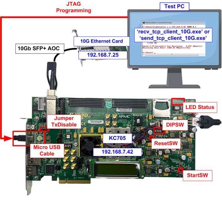
Figure 2‑1 TOE10G-IP Demo on KC705
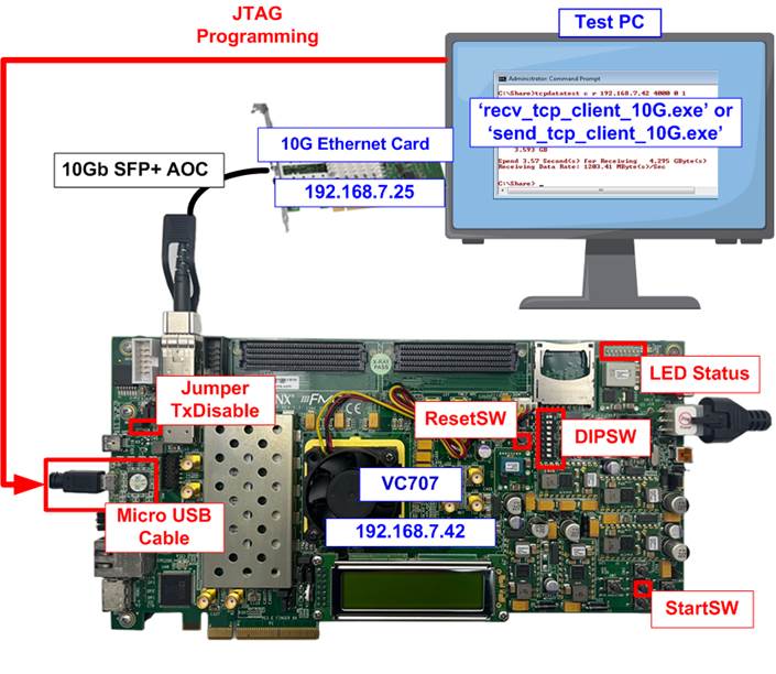
Figure 2‑2 TOE10G-IP Demo on VC707
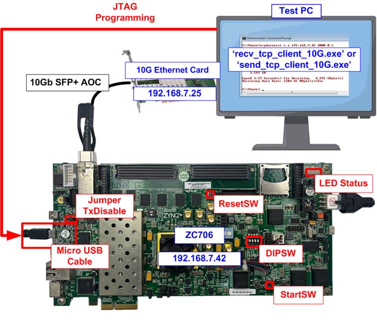
Figure 2‑3 TOE10G-IP Demo on ZC706
The steps for setting up a test environment using an FPGA and a PC are described below.
1) Check the DIP switch and jumper settings on the FPGA board.
a) For the ZC706 board, configure the settings as shown in Figure 2‑4.
- Insert a jumper at J17 to enable Tx SFP+.
- Set SW11 to all OFF to configure PS from JTAG.
- Set SW4[1:2] = �OFF ON� to use USB-JTAG.
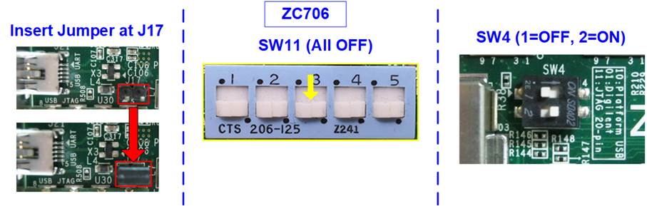
Figure 2‑4 ZC706 board setting
b) For the KC705/VC707 boards, configure the settings as shown in Figure 2‑5.
- Insert jumper J4 for the KC705 board.
- Insert jumper J6 for the VC707 board.
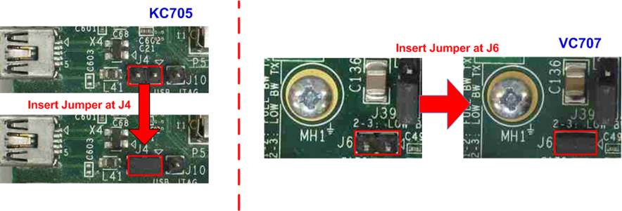
Figure 2‑5 KC705 and VC707 board setting
2) Connect a micro-USB cable from the FPGA board to the PC for JTAG programming.
3) Connect the power supply to the FPGA development board.
4) Connect the 10G Ethernet cable between the FPGA board and the PC.
5) Power on the FPGA board.
6) Download the configuration file and firmware to the FPGA board using the Vivado tool to program the configuration file, as shown in Figure 2‑6.
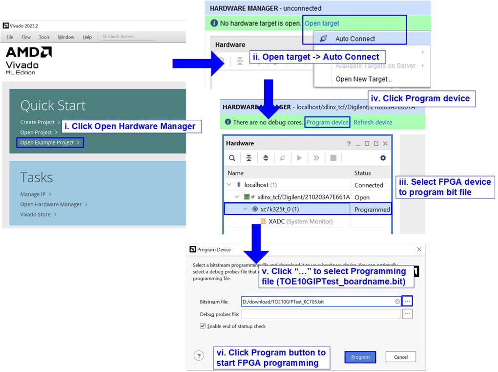
Figure 2‑6 Program FPGA by Vivado
3 PC setup
This section provides an example of setting up the 10G Network Adapter on a PC to enable Jumbo frames and optimize network performance on Windows 10 OS.
3.1 Setting the IP address
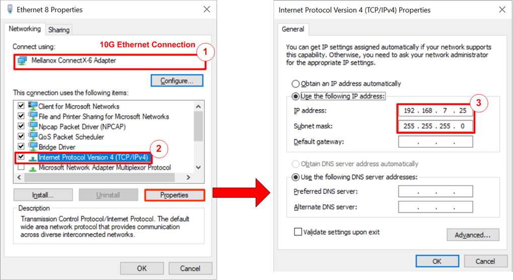
Figure 3‑1 Setting IP address on Windows OS
1) Open the Local Area Connection Properties of the 10G Ethernet connection, as shown in the left window of Figure 3‑1.
2) Select �TCP/IPv4� and click Properties.
3) Set the IP address to 192.168.7.25 and the Subnet mask to 255.255.255.0, as shown in the right window of Figure 3‑1.
3.2 Enabling Jumbo frame
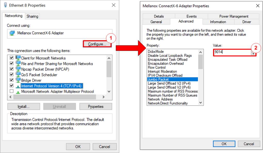
Figure 3‑2 Set frame size = Jumbo frame
1) In the Local Area Connection Properties window, click �Configure�, as shown in the left window of Figure 3‑2.
2) In the Advanced tab, select �Jumbo Packet�. Set the value to �9014 Bytes� to enable Jumbo Frame support, as shown in the right window of Figure 3‑2.
3.3 Disabling Flow Control and Interrupt Moderation
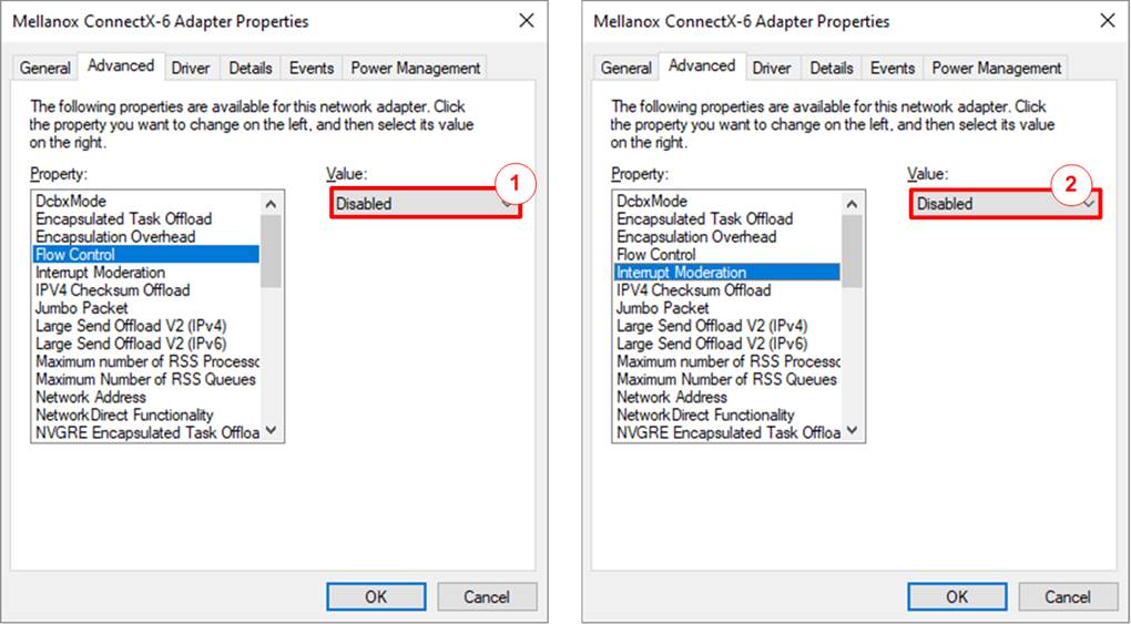
Figure 3‑3 Disable Flow Control and Interrupt Moderation
1) Select �Flow Control� and set the value to �Disabled�, as shown in the left window of Figure 3‑3.
2) Select �Interrupt Moderation� and set the value to �Disabled�, as shown in the right window of Figure 3‑3.
3.4 Checking Power Options Plan
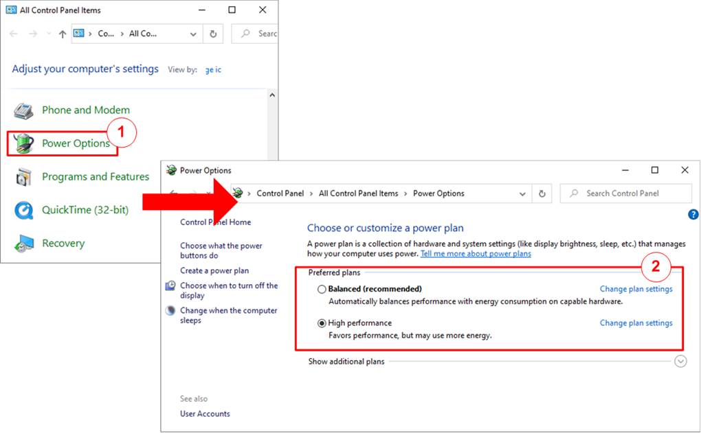
Figure 3‑4 Power options
1) Open the Control Panel and select Power Options, as shown in the left window of Figure 3‑4.
2) Change the setting to High Performance, as shown in the right window of Figure 3‑4.
4 Run Demo Test
After completely setting up the FPGA and PC as described in the previous section, this section proceeds to run the TOE10G-IP demo on real board. It shows the examples for running each test case with displaying the performance results upon the test completion.
Though the TOE10G-IP supports full-duplex data transfer, this demo is designed to show half-duplex data transfer for simple test sequence. User has the options to select the test mode: �Send data test� or �Receive data test�. It requires the different test application running on the PC for receiving data or sending data, matching the data direction from the TOE10G-IP. The user configures the test parameters such as transfer size and transfer direction through DIP switch, as defined in Table 1.
In addition, the LEDs are used to indicate the test statuses, detailed in Table 2.
Table 1 DIP Switch Settings on FPGA Development Board
|
DIPSW |
OFF |
ON |
|
Bit 1 |
Using non-Jumbo frame (1456 bytes) for Send data test |
Using Jumbo frame (8960 bytes) for Send data test |
|
Bit 2 |
Send data test |
Receive data test |
|
Bit 3 |
Disable data verification for Receive data test |
Enable data verification for Receive data test |
Table 2 LED Status on FPGA Development Board
|
GPIO LED |
ON/BLINK |
OFF |
|
0 |
ON: IP initialization complete |
Not complete. |
|
1/R |
BLINK: Operation timeout |
Normal operation |
|
2/C |
ON: Send data test with jumbo frame |
Send data test with non-jumbo frame |
|
3/L |
ON: TCP connection has been established BLINK: Data verification failed in receiving mode |
TCP connection is not established |
Note: DIPSW setting must maintain its value while the test is not completed.
The initialization steps before proceeding with data transfer are as follows.
1) Press �StartSW� on the FPGA boards to initialize the system parameters. The switch position of each FPGA board is displayed in Figure 2‑1 - Figure 2‑3.
2) Ensure the LED[0] is turned ON, indicating that the initialization is completed. The status of LED[2] depends on the value of DIPSW[1], as shown in Figure 4‑1 and Figure 4‑2. If the initialization fails, LED[1] will blink. This indicates an issue with the network parameters or hardware connections such as an incorrect target IP address or a broken Ethernet cable. Once the problem is resolved, press �ResetSW� and then �StartSW� to re-initialize the system.
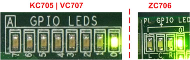
Figure 4‑1 LED Status upon the successful initialization when DIPSW[1]=OFF
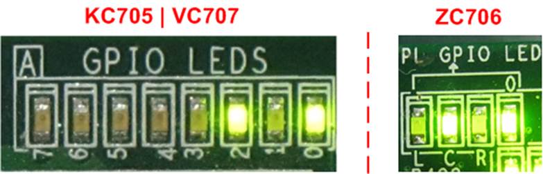
Figure 4‑2 LED Status upon the successful initialization when DIPSW[1]=ON
Examples of running the Send data test and Receive data test are described in the subsequent sections.
4.1 Send data test
To start TCP data transfer from the TOE10G-IP to the PC, set DIPSW[2] to �0�. The test application, �recv_tcp_client.exe�, is used on the PC through the Command Prompt with specified parameters for receiving data. The user sets DIPSW[1] to select the packet size: 1456 bytes or 8960 bytes, as defined in Table 1. The sequence for the Send data test is outlined as follows.
1) Ensure LED[3] is OFF, indicating no TCP data transfer.
2) Set DIPSW[1] to select the transmitted packet size: �0� for 1456 bytes (normal frame) or �1� for 8960 bytes (jumbo frame).
3) On the Command prompt at PC, input the test parameter based on DIPSW[1].
>> recv_tcp_client_10G <IP address> <Port number> <Packet size>
a) IP address: Input the FPGA IP address. This demo uses the fixed address �192.168.7.25�.
b) Port number: Input the FPGA port number. This demo uses the fixed port �4000�.
c) Packet size: Input the packet size as per the DIPSW[1] setting (1456 or 8960).
4) Once the application is executed, the TCP connection is established. During data transfer, the current amount of transferred data is displayed on the Command prompt every second.
5) Upon completion of data reception and connection termination, the total transfer size and performance are displayed on the Command prompt as the test result.
Steps 4 and 5 are iterated indefinitely for continuous data transmission. The operation can be cancelled by pressing �Ctrl+C� on the Command Prompt to halt the application execution.
Figure 4‑3 shows an example of the Send data test involving the 1456-byte data transmission (non-jumbo frame). The performance can be slightly increased by using jumbo frame size, 8960-byte packet, as shown in Figure 4‑4.
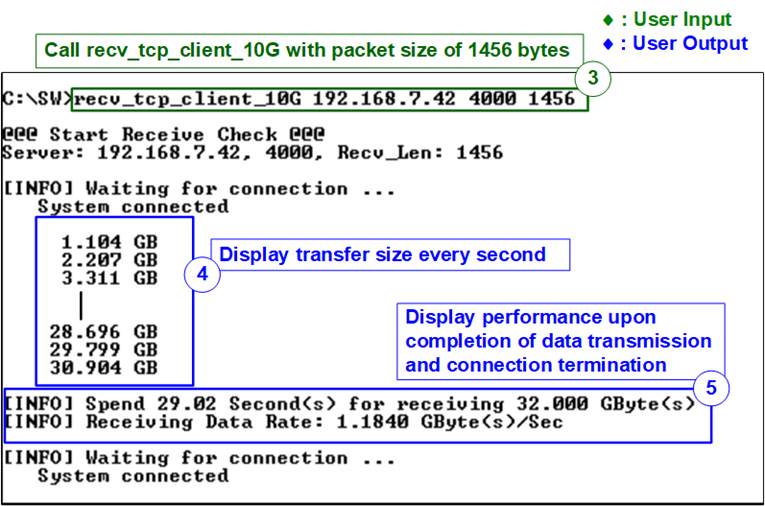
Figure 4‑3 Send data test using non-jumbo frame
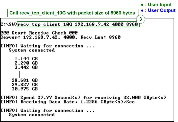
Figure 4‑4 Send data test using jumbo frame
4.2 Receive data test
To start TCP data transfer from the PC to the TOE10G-IP, set DIPSW[2] to �1�. The test application, �send_tcp_client.exe�, is used on the PC through the Command prompt with specified parameters for sending data. The user sets DIPSW[3] to enable or disable data verification, as defined in Table 1. The sequence for the Receive data test test is outlined as follows.
1) Ensure LED[3] is OFF, indicating no TCP data transfer.
2) Set DIPSW[3] to select data verification: �0� for disable or �1� for enable.
3) On the Command prompt at PC, input the test parameter based on DIPSW[3].
>> send_tcp_client_10G <IP address> <Port number> <sendlen> <pattern>
a) IP address: Input the FPGA IP address. This demo uses the fixed address �192.168.7.25�.
b) Port number: Input the FPGA Port number. This demo uses the fixed port �4000�.
c) Sendlen: Input the transfer size in 60 KB units. The valid range is 1-559241.
d) Pattern: Input the value matching the DIPSW[3] setting. Select �0� to send dummy data or �1� to send incremental data.
4) Once the application is executed, the TCP connection is established. During data transfer, the current amount of transferred data is displayed on the Command prompt every second.
5) Upon completion of data transmission and connection termination, the total transfer size and performance are displayed on the Command prompt as the test result.
Figure 4‑5 shows an example of the Receive data test with data verification enabled on FPGA development board while the PC transmits incremental data by executing the �send_tcp_client_10G.exe� application. LED[3] will blink if data verification detects an error.
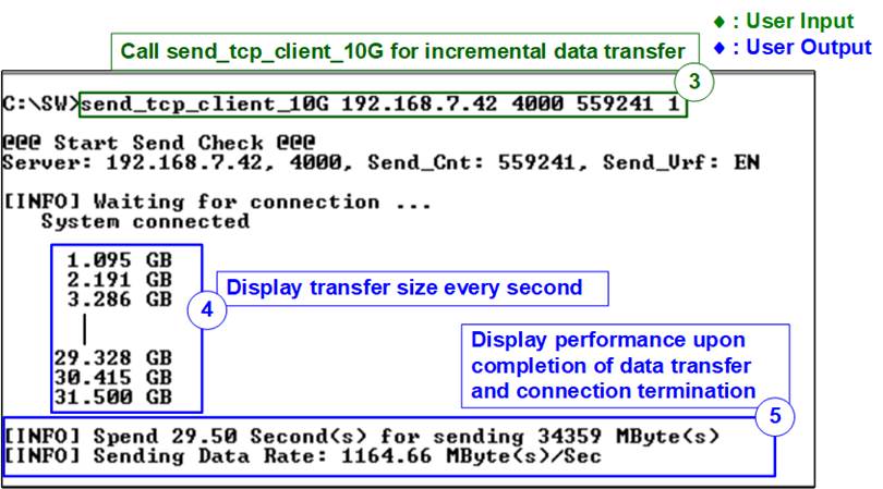
Figure 4‑5 Receive data test using incremental data transmission
The performance on the PC may be constrained by its resource while transmitting incremental data. Performance may be increased by transmitting dummy data, resulting in the best-case scenario for the test application settings, as shown in Figure 4‑6.
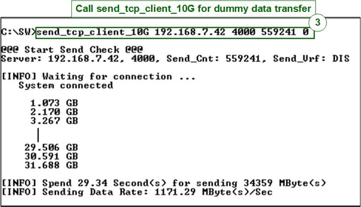
Figure 4‑6 Receive data test using dummy data transmission
5 Revision History
|
Revision |
Date |
Description |
|
1.03 |
4-Jul-24 |
Update performance |
|
1.02 |
24-Aug-15 |
Add 3.3 Power Option Setting |
|
1.01 |
10-Nov-14 |
Add ZC706 support |
|
1.00 |
5-Sep-14 |
Initial version release |