FPGA setup TOE/UDP10G-IP with CPU Demo
Rev3.2 5-Jul-23
2 Test environment setup when using FPGA and PC
3 Test environment setup when using two FPGAs
1 Overview
This document describes how to setup FPGA board and prepare the test environment for running TOE10G-IP or UDP10G-IP demo. The user can setup two test environments for transferring TCP data or UDP data via 10Gb Ethernet connection by using TOE10G-IP or UDP10G-IP, as shown in Figure 1‑1.

Figure 1‑1 Two test environments for running the demo
First uses one FPGA board and Test PC with 10Gb Ethernet card for transferring the data. TestPC runs test application to transfer data with TOE10G-IP/UDP10G-IP on FPGA - tcpdatatest for TCP/IP half-duplex test, tcp_client_txrx_40G for TCP/IP full-duplex test, or udpdatatest for UDP/IP test. Also, NiosII terminal is run on Test PC to be user interface console.
Second uses two FPGA boards which may be different board. Both boards run TOE10G-IP or UDP10G-IP demo with assigning the different initialization mode (Client or Server) for transferring data.
2 Test environment setup when using FPGA and PC
Before running the test, please prepare following test environment.
- FPGA development board: Arria10 SoC/Arria10 GX/Cyclone10 GX/Stratix10 GX (H-Tile)/Stratix10 MX development board
- PC with 10 Gigabit Ethernet or connecting with 10 Gigabit Ethernet card
- 10Gb Ethernet cable:
a) 10 Gb SFP+ Passive Direct Attach Cable (DAC) which has 1-m or less length
b) 10 Gb SFP+ Active Optical Cable (AOC)
c) 2x10 Gb SFP+ transceivers (10G BASE-R) with optical cable (LC to LC, Multimode)
d) For Stratix10 GX board/Stratix10 MX board, QSFP+ to four SFP+ cable
- micro USB cable for JTAG connection
- Test application provided by Design Gateway for running on Test PC:
TOE10G-IP: �tcpdatatest.exe� and �tcp_client_txrx_40G.exe�
UDP10G-IP: �udpdatatest.exe�
- QuartusII Programmer and NiosII command shell, installed on PC
Note: Example hardware for running the demo is listed as follows.
[1] 10G Network Adapter: Intel X520-DA2
[2] a) 10-Gigabit SFP+ AOC cable (AOC-S1S1-001)
https://www.10gtek.com/10gsfp+aoc
b) 40-Gigabit QSFP+ to 4x10-Gigabit SFP+ cable
https://www.finisar.com/active-optical-cables/fcbn510qe2cxx
[3] PC: Motherboard ASUS Z170-K, 32 GB RAM, and 64-bit Windows7 OS
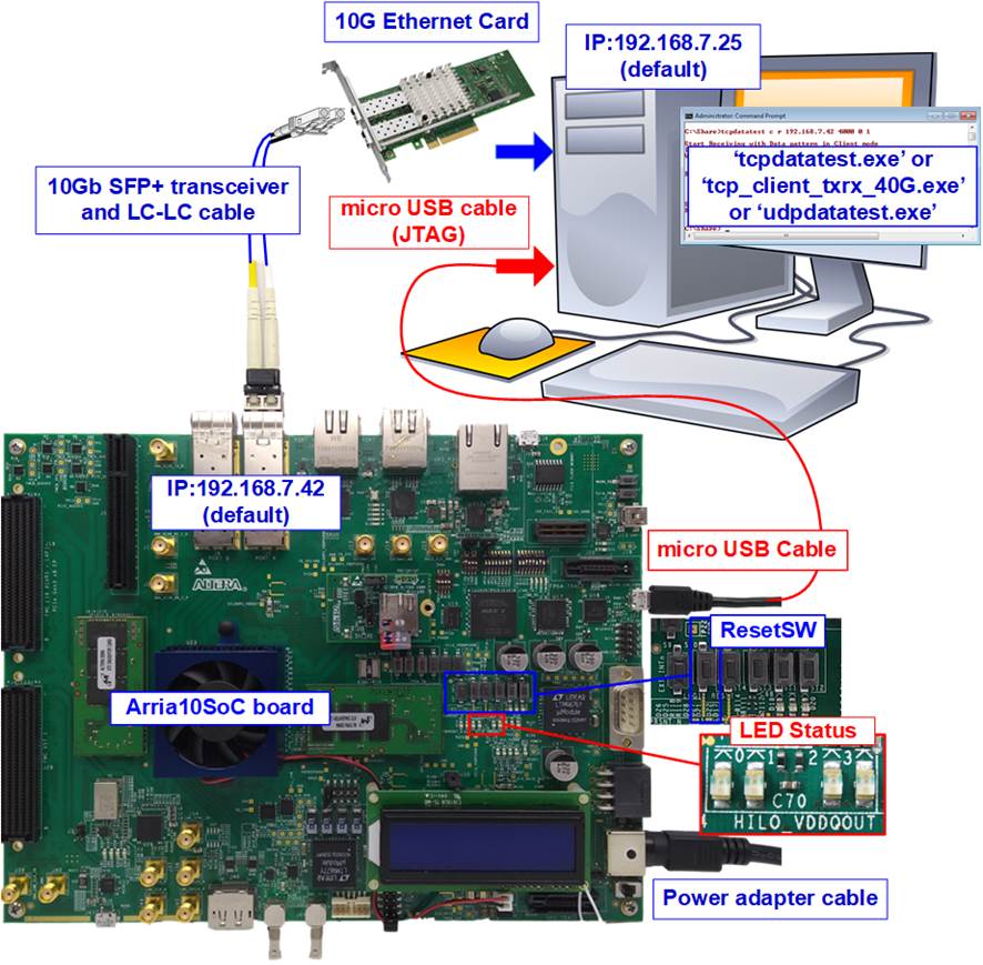
Figure 2‑1 TOE10G-IP/UDP10G-IP with CPU demo (FPGA<->PC) on Arria10 SoC
Note: Four LEDs are applied to show IP timeout status when the configuration file of the demo uses 1-hour timeout TOE10G-IP/UDP10G-IP. After running for 1 hour, the IP stops the operation. All LEDs are blinked to notify that the IP now is timeout. User needs to reconfigure FPGA to restart the test.

Figure 2‑2 TOE10G-IP/UDP10G-IP with CPU demo (FPGA<->PC) on Arria10 GX
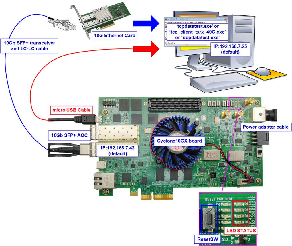
Figure 2‑3 TOE10G-IP/UDP10G-IP with CPU demo (FPGA<->PC) on Cyclone10 GX
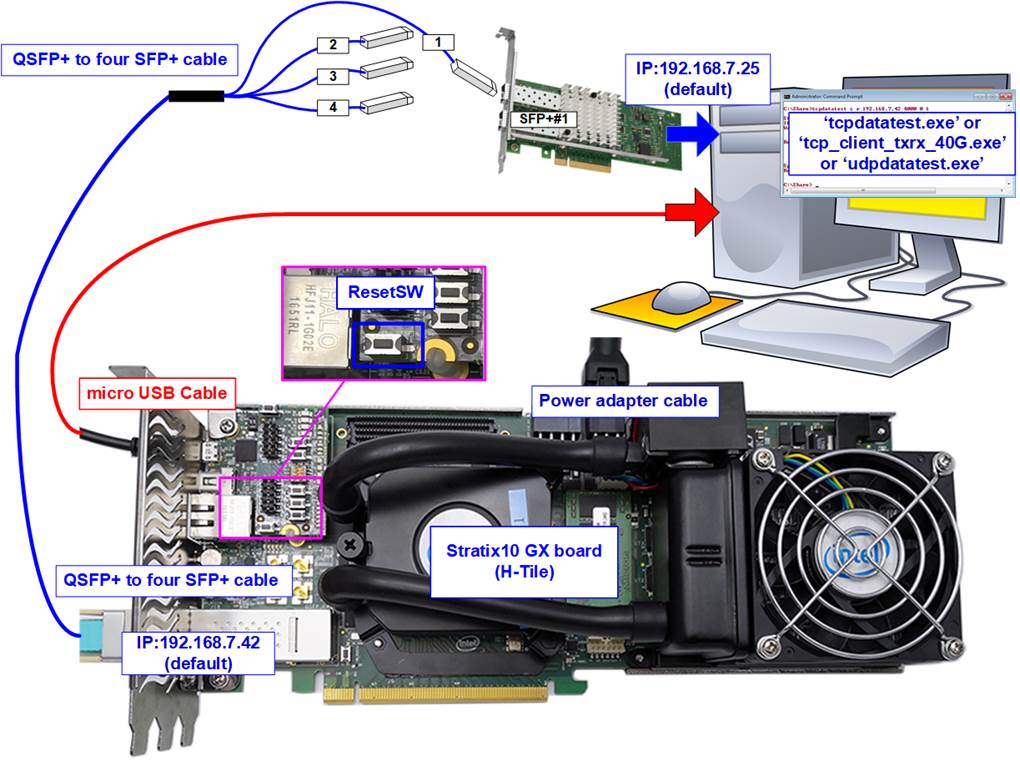
Figure 2‑4 TOE10G-IP/UDP10G-IP with CPU demo (FPGA<->PC) on Stratix10 GX

Figure 2‑5 TOE10G-IP/UDP10G-IP with CPU demo (FPGA<->PC) on Stratix10 MX
The step to setup test environment by using FPGA and PC is described in more details as follows.
1) Turn off power switch and connect power supply to FPGA board.
2) Connect micro USB cable from FPGA board to PC for JTAG programming and JTAG UART.
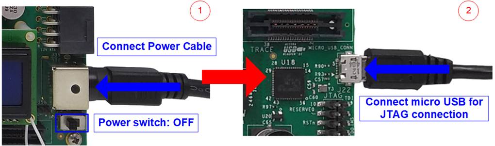
Figure 2‑6 Power connection and microUSB connection
3) Connect 10Gb Ethernet cable between FPGA board and PC.
a) For the board except Stratix10 GX and Stratix10 MX board, insert 10 Gb SFP+ DAC (Length<1m), AOC or SFP+ transceiver with LC-LC cable) between FPGA board and PC.
b) For Stratix10 GX/Stratix10 MX board, insert QSFP+ to 4 SFP+ cable between FPGA board and PC. Use SFP+ no.1 to connect to QSFP1, as shown in Figure 2‑7.
Note: Stratix10 MX board which has two QSFP28 connectors, use the right connector.
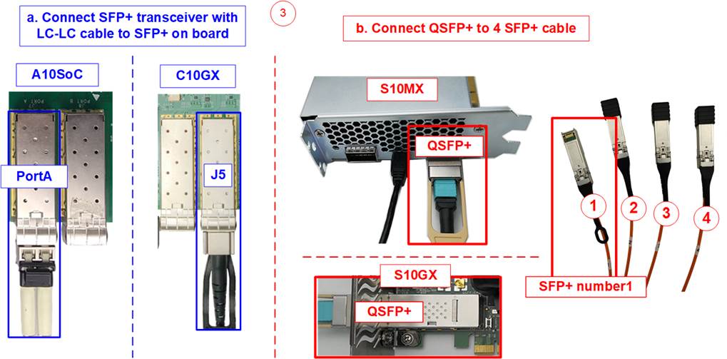
Figure 2‑7 10Gb Ethernet connection
4) Turn on power switch on FPGA board.
5) For Arria10 SoC board, set programmable clock to 322.265625 MHz by using �Clock Control� application as following step.
i. Open �Clock Controller� application.
ii. Select Si5338 tab (U50) and set CLK3 frequency = 322.265625 MHz.
iii. Click �Set� button and wait until the application is active again.
iv. Close Clock controller application.

Figure 2‑8 Reference clock programming
6) Open QuartusII Programmer to program FPGA through USB-1 by following step.
i. Click �Hardware Setup�� to select USB-BlasterII[USB-1].
ii. Click �Auto Detect� and select FPGA number.
iii. Select Arria 10/Cyclone 10/Stratix 10 device icon.
iv. Click �Change File� button, select SOF file in pop-up window and click �open� button.
v. Check �program�.
vi. Click �Start� button to program FPGA.
vii. Wait until Progress status is equal to 100%.
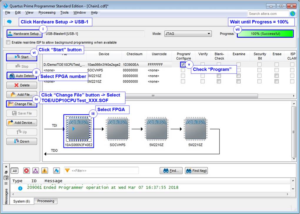
Figure 2‑9 FPGA Programmer
7) Open NiosII command shell.
i. Type �nios2-terminal� to run the console.
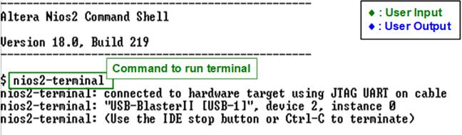
Figure 2‑10 Run NiosII terminal
ii. Input �0� to initialize TOE10G-IP/UDP10G-IP in client mode (asking PC MAC address by sending ARP request).
iii. Default parameter in client mode is displayed on the console.
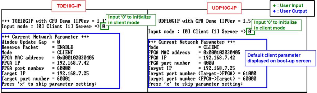
Figure 2‑11 Message after system boot-up
If Ethernet connection has the problem and the status is linked down, the error message is displayed on the console instead of welcome message, as shown in Figure 2‑12.
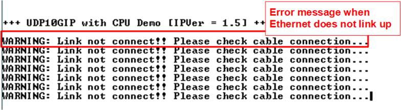
Figure 2‑12 Error message when cable is linked down
iv. User enters �x� to skip parameter setting for using default parameters to begin system initialization, as shown in Figure 2‑13. If user enters other keys, the menu for changing parameter is displayed, similar to �Reset TCPIP parameters� menu. The example when running the main menu is described in �dg_toe10gip_cpu_instruction� or �dg_udp10gip_cpu_instruction� document.
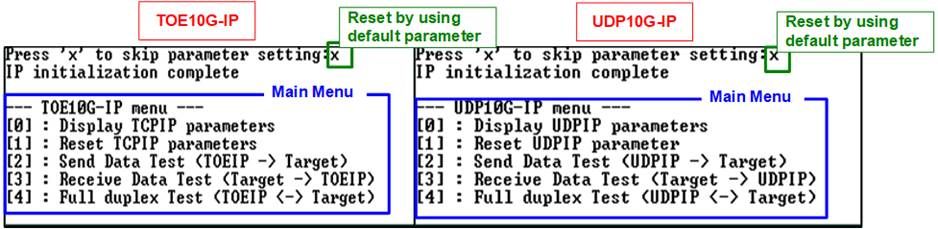
Figure 2‑13 Initialization complete
Note: Transfer performance in the demo depends on Test PC specification in Test platform. The best performance can be achieved when the test is run by using FPGA-to-FPGA connection.
3 Test environment setup when using two FPGAs
Before running the test, please prepare following test environment.
- Two FPGA development boards which are the same board or different board,
Arria10 SoC/Arria10 GX/Cyclone10 GX/Stratix10 GX (H-Tile)/Stratix10 MX development board
- 10Gb Ethernet cable:
a) 10 Gb SFP+ Active Optical Cable (AOC)
b) 2x10 Gb SFP+ transceiver (10G BASE-R) with optical cable (LC to LC, Multimode)
c) For Stratix10 GX board, QSFP+ to four SFP+ cable
- Two micro USB cables, one cable for connecting one FPGA board to PC
- QuartusII Programmer for programming FPGA and NiosII command shell, installed on PC

Figure 3‑1 TOE10G-IP/UDP10G-IP with CPU demo (FPGA<->FPGA)
The step to setup test environment by using two FPGAs is described in more details as follows.
Follow step 1) � 5) of topic 2 (Test environment setup when using FPGA and PC) to prepare FPGA board.
Warning: For Arria10 SoC board, Clock controller for programming clock to 322.265625 MHz could be used when only one FPGA is connected to PC. User connects one micro USB cable to set clock on one Arria 10 SoC board at a time. If two Arria 10 SoC boards are used in the test, user must switch micro USB cable to program clock on the 2nd board after finishing the 1st board setting. After that, two micro USB cables for connecting two FPGA boards to PC are allowed.
1) Connect 10Gb Ethernet cable between two FPGA boards.
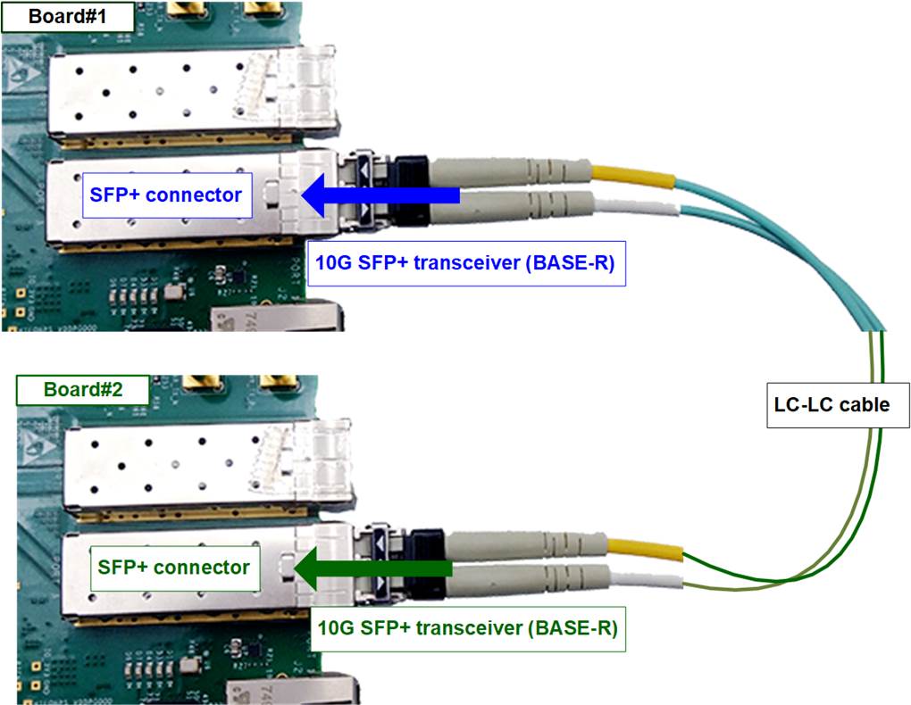
Figure 3‑2 SFP+ transceiver connection
2) Connect micro USB cable of each FPGA board to PC. After that, PC detects two USB-Blaster cables as USB-1 and USB-2 from two USB connections with two FPGA boards. Follow step 1) - 6) of topic 2 (Test environment setup when using FPGA and PC) for FPGA configuration.
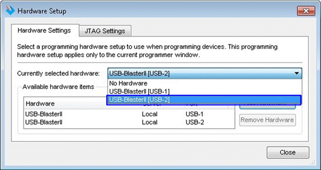
Figure 3‑3 Two USB-Blaster cables when connecting two FPGA boards to PC
3) Open QuartusII Programmer to program FPGA board#1 by using USB-1 connection and then switch to program FPGA board#2 by using USB-2 connection.

Figure 3‑4 Select USB-BlasterII
4) Open NiosII Command Shell.
i. Run nios2-terminal --cable 1 command for FPGA#1
ii. Run nios2-terminal �cable 2 command for FPGA#2
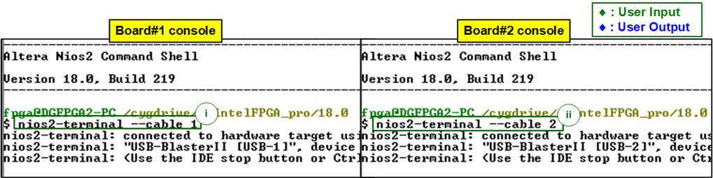
Figure 3‑5 Run NiosII terminal on two consoles
5) Set the input to the console. To initialize by Server-Client mode, run following steps.
i. Set �1� on console of FPGA board#1 for running Server mode.
ii. Set �0� on console of FPGA board#2 for running Client mode.
iii. Default parameters for Server or Client are displayed on the console, as shown in Figure 3‑6.
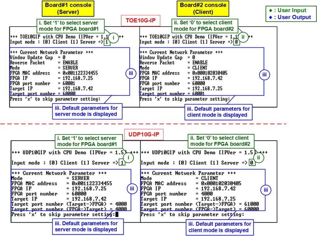
Figure 3‑6 Input mode
6) Input �x� to use default parameters or other keys to change parameters. The parameters of Server mode must be set before Client mode.
When running TOE10G-IP,
i. Set parameters on Server console.
ii. Set parameters on Client console to start IP initialization by transferring ARP packet.
iii. After finishing initialization process. �IP initialization complete� and main menu are displayed on Server console and Client console.
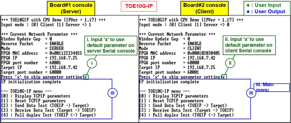
Figure 3‑7 Main menu
When running UDP10G-IP,
i. For Server mode, if user does not change default parameters, input �x� to skip parameter setting.
ii. For Client mode, user must change target port number (Target->FPGA) to use same value as target port number (FPGA->Target).
iii. After finishing initialization process, �IP initialization complete� and main menu are displayed on Server console and Client console.

Figure 3‑8 Main menu of UDP10G-IP
4 Revision History
|
Revision |
Date |
Description |
|
1.0 |
19-Mar-18 |
Initial version release |
|
1.1 |
27-Mar-18 |
Add Part A (FPGA<->PC test) |
|
1.2 |
4-Apr-18 |
Correct optical cable in Figures and the descriptions |
|
1.3 |
5-Feb-19 |
Add Arria 10 GX board and change software to tcp_client_txrx_40G |
|
1.4 |
31-May-19 |
Add timeout LED descriptions |
|
1.5 |
20-Aug-19 |
Add Cyclone10 GX board |
|
2.0 |
18-Jun-20 |
Remove test result on the console |
|
3.0 |
26-Aug-20 |
TOE10G-IP and UDP10G-IP |
|
3.1 |
4-Mar-21 |
Support S10MX board |
|
3.2 |
8-Apr-22 |
Update Figure 2‑11 and Figure 3‑6 |