1 Overview
This document shows the example to run UDP1G-IP demo by using two test environments. First is run by using one FPGA board transferring UDP data with TestPC which runs test application for transferring UDP data via 1Gb Ethernet. Test performance and data loss rate on the first environment is limited by the resource on TestPC. Second is run by using two FPGA boards for transferring 1Gb Ethernet data together. The second environment achieves the best performance for transferring UDP data via 1Gb Ethernet by using UDP1G-IP and data is not lost when the hardware signal is in good quality.
In the document, topic 2 shows the example to set up 1Gb Ethernet card on TestPC to get the good performance for transferring data via 1Gb Ethernet when running the test by using the first test environment, FPGA and Test PC. Topic 3 shows the example console and test result when running under the first test environment. Finally, topic 4 shows the example console when running the second test environment, FPGA and FPGA. More details of each topic are described as follows.
2 PC Setup
Before running the demo, please check the network setting on PC. The example for setting the network is shown as follows.
2.1 IP Setting
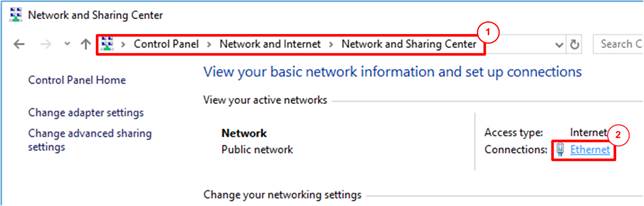
Figure 2‑1 IPv4 setting
1) Open Ethernet setting option from Control Panel -> Network and Internet -> Network and Sharing Center.
2) Click Gigabit Ethernet icon which is used to connect with FPGA board.
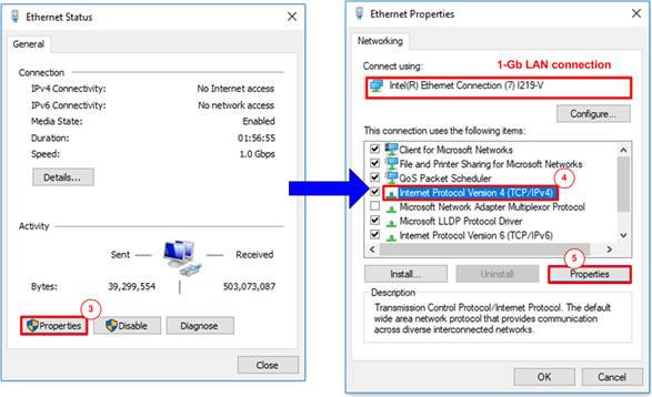
Figure 2‑2 Select IP address setting menu
3) Click Properties button in Ethernet Status window.
4) Select “TCP/IPv4”.
5) Click Properties button in Ethernet Properties window.
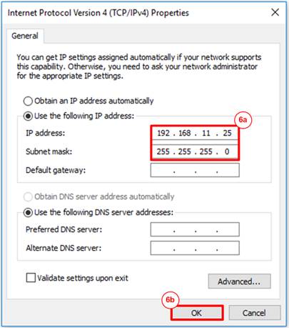
Figure 2‑3 Setting IP address for PC
6) Set IP address = 192.168.11.25 and Subnet mask = 255.255.255.0. After that, click OK button to confirm IP address setting.
2.2 Speed and Frame Setting
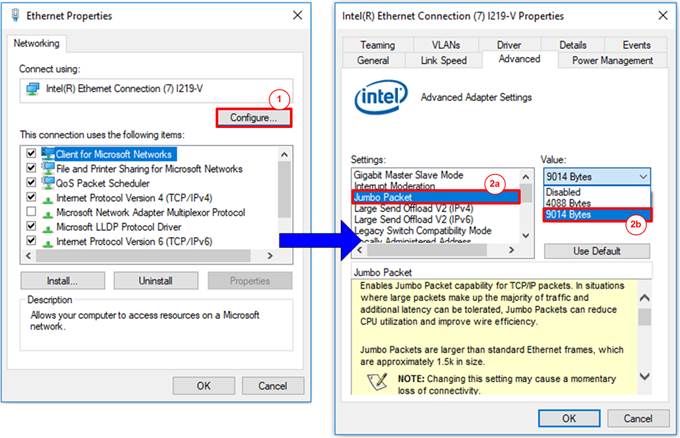
Figure 2‑4 Jumbo frame setting
1) Click Configure button in Ethernet Properties window.
2) On Advanced Tab, select “Jumbo Packet” and then set Value to “9014 Bytes” for Jumbo Frame support.
3) On Link Speed, select “1 Gbps Full Duplex” and click OK button, as shown in Figure 2‑5.
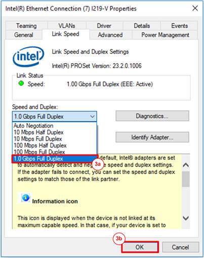
Figure 2‑5 Set link speed = 1 Gbps
2.3 Power Option Setting
1) Open Control Panel and select Power Options, as shown in the left window of Figure 2‑6.
2) Set High Performance plan, as shown in the right window of Figure 2‑6.

Figure 2‑6 Power options
2.4 Firewall Setting
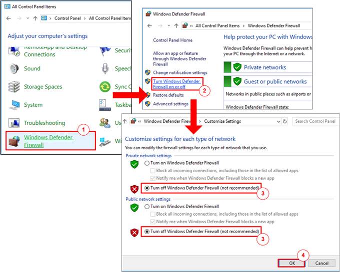
Figure 2‑7 Firewall setting
1) Open Control Panel and select Windows Firewall.
2) Click “Turn Windows Firewall on or off”.
3) Select Turn off Firewall under Private and Public network settings.
4) Click OK button to confirm the setting.
3 Test result when using FPGA and TestPC
3.1 Display UDPIP parameters
Select ‘0’ to check current parameter in the demo. There are seven parameters displayed on the console.
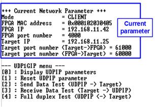
Figure 3‑1 Display current parameter result
1) Mode : Mode of UDP1G-IP to run as server or client. To run with PC, please input ‘0’ to initialize as client mode.
2) FPGA MAC address : 48-bit hex value to be MAC address of FPGA. Default value is 0x000102030405.
3) FPGA IP : IP address of FPGA. Default value is 192.168.11.42.
Note: This value is used to be FPGA IP address, parameter for test application on PC.
4) Target IP : IP address of destination device (1 Gb Ethernet on PC). Default value is 192.168.11.25.
5) FPGA port number: Port number of FPGA. Default value is 4000.
Note: This value is used to be FPGA port, parameter for test application on PC.
6) Target port number (Target->FPGA) : Port number of the destination device to send data to FPGA. Default value is 61000.
Note: This value is used to be PC port, parameter for test application on PC in transmit mode.
7) Target port number (FPGA->Target) : Port number of the destination device to receive data from FPGA. Default value is 60000.
Note: This value is used to be PC port, parameter for test application on PC in received mode.
To change some parameters, user can set by using menu [1] (Reset UDPIP parameter).
3.2 Reset UDPIP parameters
Select ‘1’ to reset the IP and change IP parameters.
This menu is used to change IP parameters or send reset to UDP1G-IP. After user selects this menu, the current parameters are displayed on the console. User inputs ‘x’ to use the same parameters or other keys to change some parameters. After the parameters are set, reset signal is sent to UDP1G-IP.
There are seven parameters to set in this menu. Each parameter is verified by CPU. The parameter is updated to UDP1G-IP when the input is valid. If the input is not valid, the parameter does not change. After user inputs all parameters, IP is reset. The description of each parameter is shown in topic 3.1 (Display ) and the range of each parameter is described as follows.
1) Mode : ‘0’ to initialize the IP as client mode.
2) FPGA MAC address : 12-digit of hex value. Add “0x” to be prefix to input as hex value.
3) FPGA IP address : A set of four decimal digits is separated by “.”. The valid range of each decimal digit is 0-255.
4) FPGA port number : Valid range is 0-65535.
5) Target IP address : A set of four decimal digits, similar to FPGA IP address. This value is IP address of Test PC.
6) Target port number (Target->FPGA) : Valid range is 0-65535.
7) Target port number (FPGA->Target) : Valid range is 0-65535.
After finishing all parameter assignment, new parameters are displayed on the console. Next, reset signal is sent to the IP for loading new parameters. Finally, “IP initialization complete” is shown after IP completes initialization process, as shown in Figure 3‑2.

Figure 3‑2 Change IP parameter result
3.3 Send Data Test
To transfer data from FPGA to PC, select ‘2’ to run send data test on FPGA and prepare “udpdatatest.exe” on PC to receive data. User sets test parameters on FPGA for sending data through the console. On PC, user sets test parameters of “udpdatatest.exe” to receive data through Command prompt. The step to run the test is described as follows.
1) On FPGA console, set two parameters under send data test menu.
a) Input transfer size: Unit of transfer size is byte. Valid value is 0x1 - 0xFFFF_FFFF. The input is decimal unit when the input is only digit number. User can add “0x” as a prefix for hexadecimal input.
b) Input packet size: Unit of packet size is byte. Valid value is 1 – 8972. The input is decimal unit when the input is only digit number. User can add “0x” as a prefix for hexadecimal input.
Note: When packet size is more than 1472, the packet output from UDP1G-IP is jumbo frame size. In this case, Test PC must support jumbo frame.
2) If all inputs are valid, the recommended parameters to run test application on PC are displayed. After that, “Press any key to start data sending ...” is displayed to begin data sending when user enters some keys.
3) On Command prompt, user runs the application by using the recommended parameters. There are five parameters for “udpdatatest”.
>> udpdatatest [Dir] [FPGAIP] [FPGAPort] [PCPort] [ByteLen] <Pattern> <Timeout>
a) Dir : Set ‘r’ to receive test data from FPGA
b) FPGA IP : Set the same value as FPGA IP address
c) FPGA port : Set the same value as FPGA port number
d) PC port : Set the same value as target port number (FPGA->Target)
e) ByteLen : Set the same value as “Input transfer size” of step 1a)
f) Pattern : ‘1’- enable data verification, ‘0’-disable data verification.
Default value is ‘1’.
g) Timeout : Timeout in msec unit. Valid value is 100-65536.
It is recommended to set to 1000 (1 sec). Default value is 100.
4) After running test application, the summary of setting parameter is displayed. After that, PC waits received data from FPGA.
5) On FPGA console, user enters any key(s) to start sending data. During transferring data, current transfer size is displayed on FPGA console (transmit size) and Command prompt (receive size) every second.
6) “Send data complete” is displayed on FPGA console after all data are sent. On PC, test application is finished by one of two conditions. First, total data have been received (no lost data is found within networking). Second is timeout condition when no additional data is received more than 1 second. After timeout is found, timeout message with the 1st error position is displayed. Finally, total transfer size and performance are displayed on FPGA console (transmit performance) and Command prompt (receive performance).
Figure 3‑3 shows the example of send data test when using non-jumbo frame size. The left window is FPGA console while the right window is Command prompt on PC.
Figure 3‑4 shows the example of send data test when using jumbo frame size. Performance when running jumbo frame is better than non-jumbo frame.

Figure 3‑3 Send data test by using non-jumbo frame
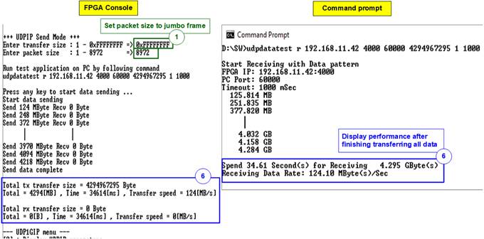
Figure 3‑4 Send data test by using jumbo frame
When some inputs are invalid, “Out-of-range input” is displayed. After that, the operation is cancelled, as shown in Figure 3‑5 - Figure 3‑6.

Figure 3‑5 Error from invalid transfer size

Figure 3‑6 Error from invalid packet size
3.4 Receive Data Test
To transfer data from PC to FPGA, select ‘3’ to run receive data test on FPGA and prepare “udpdatatest.exe” on PC to send data. User sets test parameters on FPGA for receiving data through FPGA console. On PC, user sets parameters of “udpdatatest.exe” to send data through Command prompt. The step to run the test is shown as follows.
1) On FPGA console, set two parameters under send data test menu.
a) Input transfer size: Unit of transfer size is byte. Valid value is 0x1 - 0xFFFF_FFFF. The input is decimal unit when the input is only digit number. User can add “0x” as a prefix for hexadecimal input.
b) Input data verification mode: ‘0’-disable data verification, ‘1’-enable data verification sent from PC.
2) If all inputs are valid, the recommended parameters to run test application on PC are displayed. After that, “Wait data from Target ...” is displayed on the console when IP is ready to receive data from PC.
3) On Command prompt, user runs the application by using the recommended parameters. There are five parameters for “udpdatatest”.
>> udpdatatest [Dir] [FPGAIP] [FPGAPort] [PCPort] [Bytelen]
a) Dir : Set ‘t’ to send test data from FPGA
b) FPGA IP : Set the same value as FPGA IP address
c) FPGA port : Set the same value as FPGA port number
d) PC port : Set the same value as target port number (Target->FPGA)
e) Bytelen : Set the same value as “Input transfer size” of step 1a)
4) After running test application, test application starts sending data out to FPGA. During transferring data between FPGA and PC, current transfer size is displayed on both FPGA console (receive size) and Command prompt (transmit size) every second.
5) “Receive data complete” is displayed on FPGA console after FPGA receives all data or 1-second timeout is found. Finally, total transfer size and performance are displayed on FPGA console (receive performance) and Command prompt (transmit performance).
Figure 3‑7 shows the example of receive data test when disabling data verification mode on FPGA. The left window is test result on FPGA console while the right window is test result on Command prompt.
Figure 3‑8 shows the example of receive data test when enabling data verification mode on FPGA. While PC sends incremental data to FPGA. When verification module is failed, error message is displayed.

Figure 3‑7 Receive data test without data verification
Figure 3‑8 Receive data test with enable data verification
3.5 Full duplex Test
Select ‘4’ to run full duplex test to transfer data between FPGA and PC in both directions at the same time. User sets test parameters on FPGA console. On PC, user opens two applications on two command prompts for sending and receiving data with FPGA by using different port number. The step to run the test is described as follows.
1) On FPGA console, set three parameters under full duplex test.
a) Input transfer size: Unit of transfer size is byte. Valid value is 0x1 - 0xFFFF_FFFF. The input is decimal unit when the input is only digit number. User can add “0x” as a prefix for hexadecimal unit.
b) Input packet size: Unit of packet size is byte. Valid value is 1 – 8972. The input is decimal unit when the input is only digit number. User can add “0x” as a prefix for hexadecimal unit.
c) Input data verification mode: ‘0’-disable data verification, ‘1’-enable data verification.
2) When all inputs are valid, the recommended parameters for two applications are displayed, sending data test and receiving data test.
Next, “Press any key to start data sending ...” is displayed to wait until user starts IP sending data.
3) On PC, open two Command prompts to run the test applications by using the recommended parameters.
Seven parameters are applied for the 1st Command prompt (receiving data).
>> udpdatatest [Dir] [FPGAIP] [FPGAPort] [PCPort] [ByteLen] <Pattern> <Timeout>
Five parameters are applied for the 2nd Command prompt (sending data).
>> udpdatatest [Dir] [FPGAIP] [FPGAPort] [PCPort] [ByteLen]
a) Dir : Set ‘r’ to the 1st command prompt
Set ‘t’ to the 2nd command prompt
b) FPGA IP : Set the same value as FPGA IP address
c) FPGA port : Set the same value as FPGA port number
d) PC port : Set the same value as target port number (FPGA->Target) for the 1st command prompt. Set the same value as target port number (Target->FPGA) for the 2nd command prompt.
e) Bytelen : Set the same value as “Input transfer size” of step 1a)
f) Pattern : ‘1’- enable data verification, ‘0’-disable data verification.
Default value is ‘1’.
g) Timeout : Timeout in msec unit. Valid value is 100-65536.
It is recommended to set to 1000 (1 sec). Default value is 100.
4) On FPGA console, press any key(s) to start sending data to PC. After that, current transfer size in both directions is displayed on FPGA console and two command prompts every second.
5) “Transfer data complete” is displayed on FPGA console after UDP1G-IP finishes sending and receiving all data. Finally, total transfer size and performance are displayed on FPGA console and Command prompt.
As shown in Figure 3‑9, transfer performance when running full duplex with data verification is displayed. The left window is the test result on FPGA console while the right window is the test result on Command prompt (the upper window is receive performance and the lower window is transmit performance).
Figure 3‑9 Full duplex test
4 Test result when using two FPGAs
4.1 Display UDPIP parameters
Select ‘0’ to check current parameter in the demo. There are seven parameters displayed on the console.

Figure 4‑1 Display current parameter result
1) Mode : Mode of UDP1G-IP to run as server or client.
‘0’- Client, ‘1’- Server
2) FPGA MAC address : 48-bit hex value to be MAC address of FPGA. Default value is 0x000102030405 (client mode) or 0x001122334455 (server mode).
3) FPGA IP : IP address of FPGA. Default value is 192.168.11.42 (client mode) or 192.168.11.25 (server mode).
4) FPGA port number : Port number of FPGA. Default value is 4000 (client mode) or 60000 (server mode).
5) Target IP : IP address of destination device. Default value is 192.168.11.25 (client mode) or 192.168.11.42 (server mode).
6) Target port number (Target->FPGA) : Port number of the destination device to send data to UDP1G-IP. Default value is 60001 (client mode) or 4000 (server mode).
In client mode, this value must be changed from 60001 to 60000 (the same value as default value of Target port number for FPGA -> Target).
7) Target port number (FPGA->Target) : Port number of the destination device to receive data from UDP1G-IP. Default value is 60000 (client mode) or 4000 (server mode).
To change some parameters, user can use menu [1] (Reset UDPIP parameter).
4.2 Reset UDPIP parameter
Select ‘1’ to reset the IP and change IP parameters.
This menu is applied for changing IP parameters or sending reset to UDP1G-IP. After user selects this menu, the current parameters are displayed on the console. User enters ‘x’ to use the same parameters while other keys are entered for changing some parameters. After the parameters are set, reset signal is sent to UDP1G-IP.
There are seven parameters which can be modified by user. When user enters invalid value such as ‘n’, the parameter does not change. After setting parameters completely, IP is reset.
The description of each parameter is shown in topic 4.1 (Display UDPIP parameters) and the range of each parameter is described as follows.
Note:
1. When user desires to reset parameters on server, the client FPGA must be also reset. Server must be reset firstly to wait until ARP request sent by client.
2. Target port number for sending and receiving data must be similar.
3. Parameter of client and server must be similar, i.e.
a. Target IP of server = FPGA IP of client
b. FPGA IP of server = Target IP of client
c. Target port number of server (both Tx and Rx direction) = FPGA port number of client
d. FPGA port number of server = Target port number of client (both Tx and Rx direction)
1) Mode : ‘0’- Client, ‘1’- Server.
Note: Two FPGA boards must run in different mode (one is client and another is server).
2) FPGA MAC address : 12-digit of hex value. Add “0x” as a prefix for hex input.
3) FPGA IP address : A set of four decimal digits is separated by “.”. The valid range of decimal digit is 0-255.
4) FPGA port number : Valid range is 0-65535.
5) Target IP address : A set of four decimals, similar to FPGA IP address.
6) Target port number (Target->FPGA) : Valid range is 0-65535.
7) Target port number (FPGA->Target) : Valid range is 0-65535.
After finishing all parameter assignment, new parameters are displayed on FPGA console. Next, reset signal is sent to the IP to load new parameters. Finally, “IP initialization complete” is shown after IP completes initialization process, as shown in Figure 4‑2.
Figure 4‑2 Change IP parameter result
4.3 Send and Receive data Test (Half-duplex test)
The operation to send and receive data test of server and client mode is similar. So, this topic describes the menu to transfer data between two FPGA boards. The first board runs receive data test (select menu ‘3’) and the second board runs send data test (select menu ‘2’).
User sets test parameters through FPGA console. The step to run the test is described as follows.
1) On FPGA console under menu 3 (receive data test), set two parameters.
a) Input transfer size: Unit of transfer size is byte. Valid value is 0x1 - 0xFFFF_FFFF. The input is decimal unit when the input is only digit number. User can add “0x” as a prefix for hexadecimal input.
b) Input data verification mode: ‘0’-disable data verification, ‘1’-enable data verification.
2) When all inputs are valid, “Wait data from Target ...” is displayed.
3) On FPGA console under menu 2 (send data test), set two parameters.
a) Input transfer size: Unit of transfer size is byte. Valid value is 0x1 - 0xFFFF_FFFF. The input is decimal unit when the input is only digit number. User can add “0x” as a prefix for hexadecimal input. This value must be equal to transfer size under receive data test.
b) Input packet size: Unit of packet size is byte. Valid value is 1 – 8972. The input is decimal unit when the input is only digit number. User can add “0x” as a prefix for hexadecimal input.
Note: When packet size is more than 1472, the packet output from UDP1G-IP is jumbo frame. User needs to confirm that network device supports jumbo frame when two FPGA boards connect through the network device.
4) If all inputs are valid, “Press any key to start data sending ...” is displayed. User enters some key(s) to start sending data.
5) During transferring data, current transfer size is displayed on both FPGA consoles every second.
6) “Send data complete” or “Receive data completed” are displayed on FPGA console after finishing transferring all data. Finally, total transfer size and performance are displayed on both FPGA consoles.
Figure 4‑3 shows the example to transfer data between two FPGAs by using non-jumbo frame size. Left window is FPGA console from FPGA running receive data test and right window is FPGA console from FPGA running send data test.
Figure 4‑4 shows the example of transfer data between two FPGAs by using jumbo frame size. When using jumbo frame size, performance is better than non-jumbo frame.
When some inputs are invalid, “Out-of-range input”/”Invalid input” is displayed and the operation is cancelled, as shown in Figure 3‑5 - Figure 3‑6 (similar to FPGA<->PC test).

Figure 4‑3 Send/receive data test by using non-jumbo frame
Figure 4‑4 Send data test by using jumbo frame
4.4 Full duplex Test
Select ‘4’ to run full duplex test by two FPGAs transferring data in both directions at the same time and the same port number. User sets test parameters through NiosII command shell. Firmware in the demo is designed to start full duplex by server FPGA before client FPGA. The step to run the test is shown as follows.
1) On server NiosII command shell, set three parameters under full duplex test.
a) Input transfer size: Unit of transfer size is byte. Valid value is 0x1 - 0xFFFF_FFFF. The input is decimal unit when the input is only digit number. User can add “0x” as a prefix for hexadecimal input.
b) Input packet size: Unit of packet size is byte. Valid value is 1 – 8972. The input is decimal unit when the input is only digit number. User can add “0x” as a prefix for hexadecimal input.
c) Input data verification mode: ‘0’-disable data verification, ‘1’-enable data verification sent from PC.
2) When all inputs are valid, “Wait data from Target …” is displayed.
3) On client NiosII command shell, set three parameters under full duplex test.
a) Input transfer size: Unit of transfer size is byte. Valid value is 0x1 - 0xFFFF_FFFF. The input is decimal unit when the input is only digit number. User can add “0x” as a prefix for hexadecimal input. This input must be same as transfer size input of server FPGA.
b) Input packet size: Unit of packet size is byte. Valid value is 1 – 8972. The input is decimal unit when the input is only digit number. User can add “0x” as a prefix for hexadecimal input.
c) Input data verification mode: ‘0’-disable data verification, ‘1’-enable data verification sent from PC.
4) When all inputs are valid, “Press any key to start data transfer ..” is displayed. After that, user enters some key(s) to start full duplex test.
5) During transferring data, current transfer size is displayed on both NiosII command shells every second.
6) “Transfer data complete” is displayed on both NiosII command shells. Finally, total transfer size and performance are displayed on both NiosII command shells.
Figure 4‑5 and Figure 4‑6 show full duplex test when running by using non-jumbo frame and jumbo frame size. The left window is NiosII command shell of server FPGA while the right window is NiosII command shell of client FPGA.
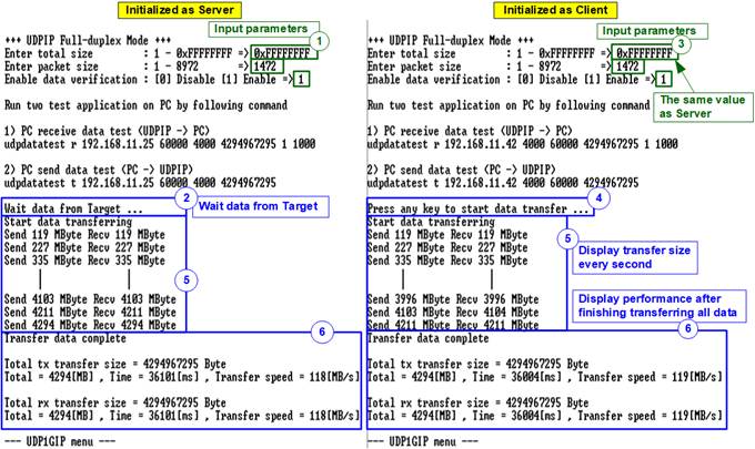
Figure 4‑5 Full duplex test when using non-jumbo frame
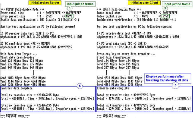
Figure 4‑6 Full duplex test when using jumbo frame
5 Revision History
|
Revision |
Date |
Description |
|
1.0 |
3-Mar-17 |
Initial version release |
|
2.0 |
10-Nov-20 |
Remove hardware setup from the document |