Rev1.2 7-Jul-23
3.6 Function list in User application
1 Introduction
Comparing to TCP protocol, UDP protocol provides a procedure to send data with a minimum of protocol mechanism, but the data cannot guarantee to be accepted by the destination because of no handshaking dialogues providing in UDP mechanism. Similar to TCP protocol, UDP protocol provides checksums for data integrity and port numbers for addressing different functions at the source and the destination in the communication networks.
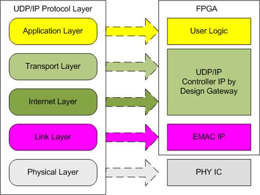
Figure 1‑1 UDP/IP Protocol Layer
UDP1G-IP implements Transport and Internet layer of UDP/IP Protocol. To send data, UDP40G-IP prepares UDP data from user logic, adds UDP/IP header to generate Ethernet packet, and sends to EMAC. To receive data, UDP40G-IP extracts UDP data and header from Ethernet packet. When UDP/IP header in the packet is valid, UDP data is stored to the buffer for user logic reading. The lower layer protocols are implemented by EMAC-IP from Intel FPGA and external PHY chip.
This reference design provides evaluation system which includes simple user logic to send and receive data by using UDP1G-IP. For user interface, CPU system is designed to interface with user through JTAG UART. The firmware is designed as bare-metal OS (no operating system). The test application software (�udpdatatest.exe�), run on PC, is also designed for sending and receiving UDP/IP packet with UDP1G-IP. The reference design is available on Intel FPGA development board to show ultra-speed data transferring. More details of the demo are described as follows.
2 Hardware overview
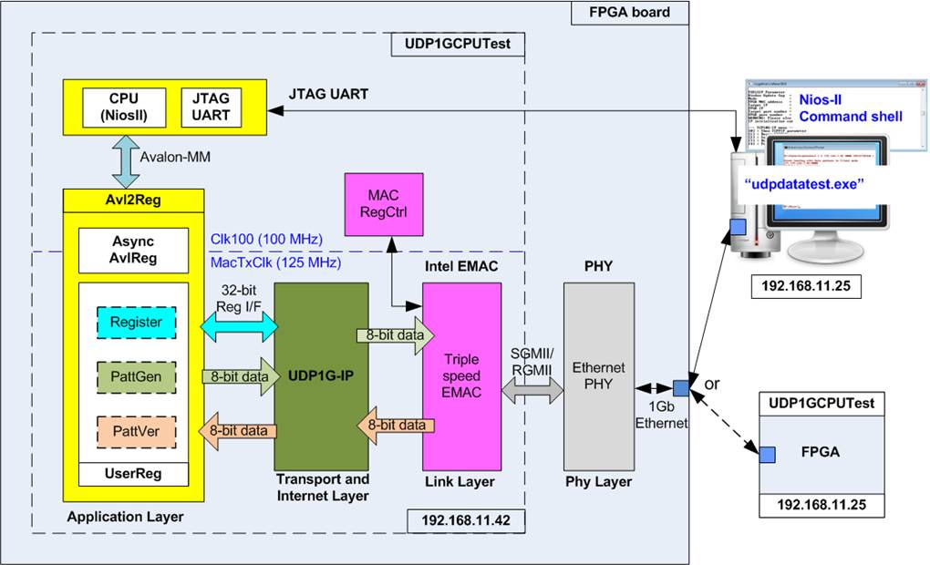
Figure 2‑1 Hardware architecture reference design
UDP1G-IP needs to connect to Triple-Speed Ethernet MAC and Ethernet PHY which implement lower-layer protocol. The user interfaces of UDP1G-IP are connected to UserReg for both control and data interface. For data interface, UserReg includes PattGen logic to generate test pattern for sending data and VerifyPatt logic to generate test pattern for verifying received data. Test pattern generated in UserReg is 32-bit incremental pattern.
For control interface, UserReg includes register to store parameters from user such as transfer length and transfer mode which are set through JTAG UART. CPU converts the user parameters to be value for setting to hardware register through Avalon bus. Due to the fact that CPU system and UDP1G-IP run in different clock domain, AsyncAvlReg module is applied to be asynchronous circuit to support clock-crossing function and then convert Avalon bus signal which is standard bus in CPU system to be register interface. CPU in the demo is NiosII and runs on bare-metal OS. CPU system includes JTAG UART hardware for user interface and timer to measure transfer performance.
2.1 External PHY
Ethernet PHY is implemented by external PHY chip. The interface of external PHY chip must be matched to Ethernet MAC. PHY Interface could be selected to be GMII, RGMII (CycloneV E board and ArriaV GX Starter board), or SGMII (Cyclone10 GX and Arria10 SoC board). Ethernet speed is fixed to 1 Gbps mode.
2.2 Triple speed Ethernet MAC
Link layer and PCS/PMA are implemented by Triple-speed Ethernet MAC, provided by Intel FPGA. EMAC has two user interfaces, i.e. Avalon stream for transferring data and Avalon-MM for configuration. In reference design, Avalon stream of EMAC is connected to UDP1G-IP while Avalon-MM interface is connected to MACRegCtrl module. The details about the register for EMAC configuration are described in �Configuration Register Space� topic within �Triple-Speed Ethernet MegaCore Function User Guide� document, provided by Intel.
https://www.intel.com/content/dam/www/programmable/us/en/pdfs/literature/ug/ug_ethernet.pdf
2.3 MACRegCtrl
This module is designed to configure parameter of Triple Ethernet MAC and monitor EMAC status through Avalon-MM bus. The logic is simply designed by using state machine. This module runs once after system power up to initialize Ethernet MAC.
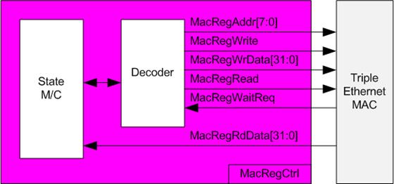
Figure 2‑2 MACRegCtrl block diagram
The sequence of initialization sequence is below.
1) Disable transmit and receive path of EMAC
2) Set software reset
3) Set frame length to support jumbo frame
4) Set Tx IFG length
5) Enable transmit and receive path of EMAC
For SGMII mode, the configuration step completes in step 5. Step 6 is necessary for RGMII mode to enable Receive/Transmit timing control function through MDIO.
6) Enable RGMII timing control
2.4 UDP1G-IP
UDP1G-IP implements UDP/IP stack and offload engine. Control and status signals are designed by register interface. Data interface is designed by FIFO interface. More details are described in datasheet.
https://dgway.com/products/IP/UDP-IP/dg_udp1gip_data_sheet_intel_en.pdf
2.5 CPU and Peripherals
32-bit Avalon-MM is applied to be the bus interface for the CPU accessing the peripherals such as Timer and JTAG UART. To control and monitor the test system, the control and status signals are connected to register for CPU access as a peripheral through 32-bit Avalon-MM bus. CPU assigns the different base address and the address range to each peripheral for accessing the internal registers of the peripheral.
In the reference design, the CPU system is built with one additional peripheral to access the test logic. The base address and the range for accessing the test logic are defined in the CPU system. So, the hardware logic must be designed to support Avalon-MM bus standard for writing and reading the register. Avl2Reg module is designed to connect the CPU system as shown in Figure 2‑3.
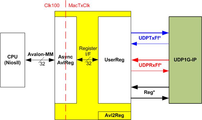
Figure 2‑3 Avl2Reg block diagram
Avl2Reg consists of AsyncAvlReg and UserReg. AsyncAvlReg is designed to convert the Avalon-MM signals to be the simple register interface which has 32-bit data bus size (similar to Avalon-MM data bus size). Otherwise, AsyncAvlReg includes asynchronous logic to support clock crossing between Clk100 domain and MacTxClk domain.
UserReg includes the register file of the parameters and the status signals. Also, data interface and control interface of UDP1G-IP are connected to UserReg. More details of AsyncAvlReg and UserReg are described as follows.
2.5.1 AsyncAvlReg

Figure 2‑4 AsyncAvlReg Interface
The signal on Avalon-MM bus interface can be split into three groups, i.e. Write channel (blue color), Read channel (red color) and Shared control channel (black color). More details of Avalon-MM interface specification are described in following document.
https://www.intel.com/content/dam/www/programmable/us/en/pdfs/literature/manual/mnl_avalon_spec.pdf
According to Avalon-MM specification, only one command (write or read) can be operated at a time. The logics inside AsyncAvlReg are split into three groups, i.e. Write control logic, Read control logic, and Flow control logic. Flow control logic to control SAvlWaitReq is applied to hold the next request from Avalon-MM interface while the current request is operating. Write control I/F and Write data I/F of Avalon-MM bus are latched and transferred as Write register. On the other hand, Read control I/F and Read data I/F of Avalon-MM bus are latched and transferred as Read register. Address I/F of Avalon-MM is latched and transferred to Address register interface as well.
The simple register interface is designed to be compatible to general RAM interface for write transaction. The read transaction of the register interface is slightly modified from RAM interface by adding RegRdReq and RegRdValid signal. The address of register interface is shared for write and read transaction. So, user cannot write and read the register at the same time. The timing diagram of the register interface is shown in Figure 2‑5

Figure 2‑5 Register interface timing diagram
1) To write register, the timing diagram is the same as general RAM interface. RegWrEn is asserted to �1� with the valid RegAddr (Register address in 32 bit unit), RegWrData (write data of the register), and RegWrByteEn (the write byte enable). Byte enable has four bits to be the byte data valid, i.e. bit[0] for RegWrData[7:0], bit[1] for RegWrData[15:8], and so on.
2) To read register, AsyncAvlReg asserts RegRdReq to �1� with the valid value of RegAddr. 32-bit data must be returned after receiving the read request. The slave must monitor RegRdReq signal to start the read transaction.
3) The read data is returned on RegRdData bus by the slave with asserting RegRdValid to �1�. After that, AsyncAvlReg forwards the read value to SAvlRead interface.
2.5.2 UserReg
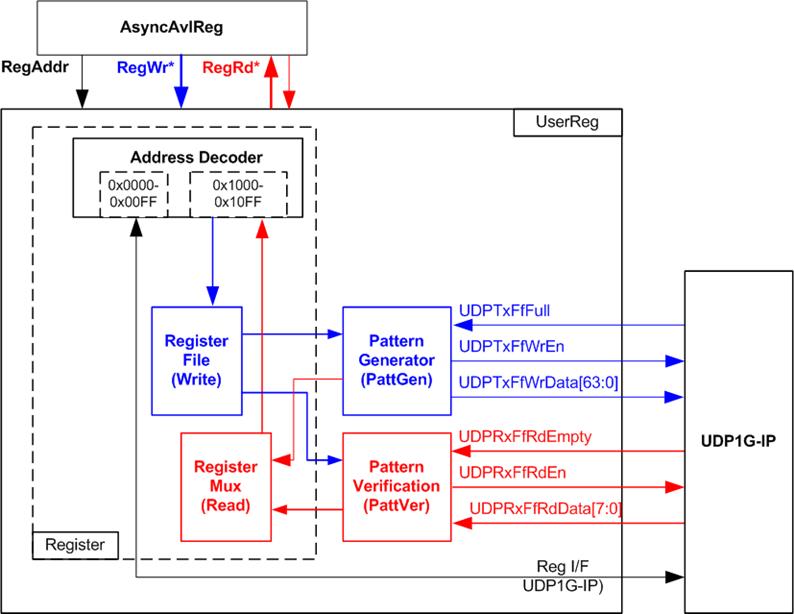
Figure 2‑6 UserReg block diagram
The logic inside UserReg has three operations, i.e. Register, Pattern generator (PattGen), and Pattern verification (PattVer). Register block decodes the address requested from AsyncAvlReg and then selects the active register for write or read transaction. Pattern generator block is designed to send 8-bit test data to UDP1G-IP following FIFO interface standard. Pattern verification block is designed to read and verify 8-bit data from UDP1G-IP following FIFO interface standard. More details of each block are described as follows.
Register Block
The address range to map to UserReg is split into two areas, i.e. UDP1G-IP register (0x0000-0x00FF) and UserReg register (0x1000-0x10FF).
Address decoder decodes the upper bit of RegAddr for selecting the active hardware. The register file inside UserReg is 32-bit bus size, so write byte enable (RegWrByteEn) is not used. To set the parameters in the hardware, the CPU must use 32-bit pointer to force 32-bit valid value of the write data.
To read register, one multiplexer is designed to select the read data within each address area. The lower bit of RegAddr is applied in each Register area to select the data. Next, the address decoder uses the upper bit to select the read data from each area for returning to CPU. Totally, the latency of read data is equal to one clock cycle, so RegRdValid is created by RegRdReq with asserting one D Flip-flop. More details of the address mapping within UserReg module is shown in Table 2‑1.
Table 2‑1 Register map Definition
|
Address |
Register Name |
Description |
|
Wr/Rd |
(Label in the �udp1gip_demo.c� ) |
|
|
BA+0x0000 � BA+0x00FF: UDP1G-IP Register Area (BA=0x0030_0000) More details of each register are described in Table2 of UDP1G-IP datasheet. |
||
|
BA+0x00 |
UDP_RST_REG |
Mapped to RST register within UDP1G-IP |
|
BA+0x04 |
UDP_CMD_REG |
Mapped to CMD register within UDP1G-IP |
|
BA+0x08 |
UDP_SML_REG |
Mapped to SML register within UDP1G-IP |
|
BA+0x0C |
UDP_SMH_REG |
Mapped to SMH register within UDP1G-IP |
|
BA+0x10 |
UDP_DIP_REG |
Mapped to DIP register within UDP1G-IP |
|
BA+0x14 |
UDP_SIP_REG |
Mapped to SIP register within UDP1G-IP |
|
BA+0x18 |
UDP_DPN_REG |
Mapped to DPN register within UDP1G-IP |
|
BA+0x1C |
UDP_SPN_REG |
Mapped to SPN register within UDP1G-IP |
|
BA+0x20 |
UDP_TDL_REG |
Mapped to TDL register within UDP1G-IP |
|
BA+0x24 |
UDP_TMO_REG |
Mapped to TMO register within UDP1G-IP |
|
BA+0x28 |
UDP_PKL_REG |
Mapped to PKL register within UDP1G-IP |
|
BA+0x38 |
UDP_SRV_REG |
Mapped to SRV register within UDP1G-IP |
|
BA+0x3C |
UDP_VER_REG |
Mapped to VER register within UDP1G-IP |
|
BA+0x1000 � BA+0x10FF: UserReg control/status (BA=0x0030_0000) |
||
|
BA+0x1000 |
Total transmit length |
Wr [31:0] � Total transmit byte size. Valid from 1-0xFFFFFFFF. Rd [31:0] � Current transmitted byte size. The value is cleared to 0 when USER_CMD_REG is written by user. |
|
Wr/Rd |
(USER_TXLEN_REG) |
|
|
BA+0x1004 |
User Command |
Wr [0] � Start Transmitting. Set �0� to start transmit data from UserReg. [1] � Data Verification enable (�0�: Disable data verification, �1�: Enable data verification) Rd [0] � UserReg busy from transmitting data (�0�: Idle, �1�: Busy) [1] � Verification fail (�0�: No error, �1�: Data verification is failed). This bit is auto-cleared when user starts new operation or reset. |
|
Wr/Rd |
(USER_CMD_REG) |
|
|
BA+0x1008 |
User Reset |
Wr [0] � Reset user logic. Set �1� to reset to UserReg. This bit is auto-cleared to �0�. [8] � Set �1� to clear TimerInt latched value. Rd [8] � Latched value of TimerInt output from IP (�0�: Normal, �1�: TimerInt=�1� is detected) This flag can be cleared by system reset condition or setting USER_RST_REG[8]=�1�. [16] � Ethernet linkup status from Ethernet MAC (�0�: Not linkup, �1�: Linkup) |
|
Wr/Rd |
(USER_RST_REG) |
|
|
BA+0x100C |
FIFO status |
Rd [15:0] � Mapped to UDPRxFfRdCnt signal of UDP1G-IP [24] � Mapped to UDPTxFfFull signal of UDP1G-IP |
|
Rd |
(USER_FFSTS_REG) |
|
|
BA+0x1010 |
Total receive length |
Rd [31:0] � Current received byte size. The value is cleared to 0 when USER_CMD_REG is written by user. |
|
Rd |
(USER_RXLEN_REG) |
|
Pattern Generator
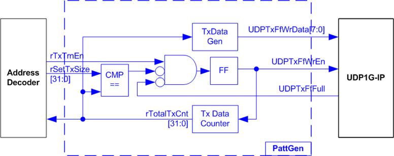
Figure 2‑7 PattGen block

Figure 2‑8 PattGen Timing diagram
PattGen is designed to generate test data to UDP1G-IP. rTxTrnEn is asserted to �1� when USER_CMD_REG[0] is set to �0�. When rTxTrnEn is �1�, UDPTxFfWrEn is controlled by UDPTxFfFull. UDPTxFfWrEn is de-asserted to �0� when UDPTxFfFull is �1�. rTotalTxCnt is the data counter to check total data sent to UDP1G-IP. rTotalTxCnt is also used to generate 32-bit incremental data to UDPTxFfWrData signal. rTxTrnEn is de-asserted to �0� when finishing transferring total data (total data is set by rSetTxSize).
Pattern Verification
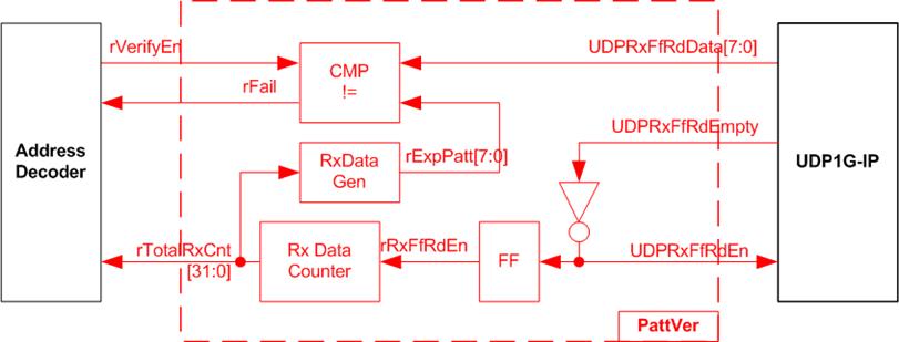
Figure 2‑9 PattVer block
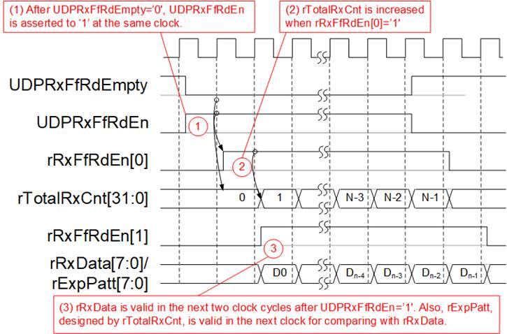
Figure 2‑10 PattVer Timing diagram
PattVer is designed to read test data from UDP1G-IP with or without data verification, depending on rVerifyEn flag. When rVerifyEn is set to �1�, data comparison is enabled to compare read data (rRxData which is one clock delay of UDPRxFfRdData) to the expected pattern (rExpPatt). When data verification is failed, rFail is asserted to �1�. UDPRxFfRdEn is designed by using NOT logic of UDPRxFfRdEmpty. UDPRxFfRdData is valid for data comparison in the next clock. rRxFfRdEn[0] which is one clock latency of UDPRxFfRdEn is applied to be counter enable of rTotalRxCnt to count total transfer size. rTotalRxCnt is used to generate rExpPatt.
3 CPU Firmware Sequence
After FPGA boot-up, welcome message is displayed. 1G Ethernet link up status (USER_RST_REG[16]) is monitored until link-up is found. Next, user selects the operation mode of UDP1G-IP to be client or server mode.
To initialize as client mode, UDP1G-IP sends ARP request to get the MAC address from the destination device. For server mode, UDP1G-IP waits ARP request to decode MAC address and returns ARP reply to complete initialization process.
If test environment uses two FPGA boards, the operation mode on two UDP1G-IPs must be different (one is client and another is server). To run with PC, it is recommended to set FPGA as client mode. When PC receives ARP request, PC always returns ARP reply. It is not simple to force PC sending ARP request to FPGA.
The software has two default parameters for each operation mode. Figure 3‑1 shows the example of the initialization sequence after system boot-up.

Figure 3‑1 Example of initialization sequence in client mode on NiosII command shell
There are four steps to complete initialization sequence as follows.
1) CPU receives the operation mode from user and displays default parameters on the console.
2) User inputs �x� to complete initialization sequence by using default parameters. Other keys are set for changing some parameters. More details for changing some parameters are described in Reset IP menu (topic 3.2).
3) CPU waits until UDP1G-IP finishing initialization sequence (UDP_CMD_REG[0]=�0�).
4) Main menu is displayed. There are five test operations for user selection. More details of each menu are described as follows.
3.1 Show parameters
This menu is used to show current parameters of UDP1G-IP, i.e. operation mode, source MAC address, destination IP address, source IP address, destination port, and source port. The step to display parameters is as follows.
1) Read all network parameters from each variable in firmware.
2) Print out each variable.
3.2 Reset IP
This menu is used to change UDP1G-IP parameters such as IP address and source port number. After setting updated parameter to UDP1G-IP register, the CPU resets the IP to re-initialize by using new parameters. Finally, the CPU monitors busy flag to wait until the initialization is completed. The step to reset IP is as follows.
1) Display current parameter value to the console.
2) Receive new input parameters from user and check input value whether valid or not. When the input is invalid, the old value is used instead.
3) Force reset to IP by setting UDP_RST_REG[0]=�1�.
4) Set all parameters to UDP1G-IP register such as UDP_SML_REG, UDP_DIP_REG.
5) De-assert UDP1G-IP reset by setting UDP_RST_REG[0]=�0�.
6) Clear PattGen and PattVer logic by sending reset to user logic (USER_RST_REG[0]=�1�).
7) Monitor IP busy flag (UDP_CMD_REG[0]) until the initialization process is completed (busy flag is de-asserted to �0�).
3.3 Send data test
Two user inputs are received to set total transmit length and packet size. The operation is cancelled if some inputs are invalid. During the test, 32-bit incremental data is generated from the logic and sent to PC or FPGA. Data is verified by Test application on PC (in case of PC <-> FPGA) or verification module in FPGA (in case of FPGA <-> FPGA). The operation is finished when total data are transferred from FPGA to PC or FPGA. The step to run send data test is as follows.
1) Receive transfer size and packet size from user and verify that all inputs are valid.
2) Set UserReg registers, i.e. transfer size (USER_TXLEN_REG), reset flag to clear initial value of test pattern (USER_RST_REG[0]=�1�), and command register to start data pattern generator (USER_CMD_REG=0). After that, test pattern generator in UserReg sends data to UDP1G-IP.
3) Display recommended parameter of test application running on PC from the current system parameters.
4) Set parameters to UDP1G-IP to start operation. Packet size is set to UDP_PKL_REG and total size is set to UDP_TDL_REG. Finally, UDP_CMD_REG is set to 1 to start IP sending data.
5) Wait until UDP1G-IP completes operation by monitoring IP busy flag (UDP_CMD_REG[0]) =�0�. During monitoring busy flag, CPU reads current transfer size from user logic (USER_TXLEN_REG) and displays on the console every second.
6) Calculate performance and show test result on the console.
3.4 Receive data test
User sets total received size and data verification mode (enable or disable). The operation is cancelled when some inputs are invalid. During the test, 32-bit incremental data is generated to verify the received data from PC or FPGA when data verification mode is enabled. The step to run receive data test is as follows.
1) Receive total transfer size and data verification mode from user input. After that, verify that all inputs are valid.
2) Set UserReg registers, i.e. reset flag to clear initial value of test pattern (USER_RST_REG[0]=�1�) and data verification mode (USER_CMD_REG[1]=�0� or �1�).
3) Display recommended parameter (similar to Step 3 of Send data test).
4) Wait until IP receives the first packet by monitoring current received size (USER_RXLEN_REG) not equal to �0�. Start timer after receiving the first packet.
5) Wait until the received size (USER_RXLEN_REG) does not change more than 1 sec or total data are received. During monitoring the received size, CPU reads current received size from user logic (USER_RXLEN_REG) and displays on the console every second.
6) Stop timer. Check interrupt from timeout (USER_RST_REG[8]) and data verification flag (USER_CMD_REG[1]) register when verification mode is applied. When the error is detected, the error message is displayed.
7) Calculate performance and show test result on the console.
3.5 Full duplex test
This menu is designed to run full duplex test by transferring data between FPGA and PC/FPGA in both directions at the same time. Three inputs are received from user, i.e. total size for both directions, packet size for FPGA sending logic, and data verification mode for FPGA receiving logic.
When running the test by using PC and FPGA, user must open �udpdatatest� application two times on two consoles. First application is for receiving data with FPGA and another application is for sending data with FPGA. The port using in two applications must be different.
When running full duplex test by using two FPGAs, one port is applied for both sending and receiving data. The step to run the test is as follows.
1) Receive total data size, packet size, and data verification mode from user and verify that all inputs are valid.
2) Set UserReg registers, i.e. transfer size (USER_TXLEN_REG), reset flag to clear initial value of test pattern (USER_RST_REG), and command register to start data pattern generator with data verification mode (USER_CMD_REG=1 or 3).
3) Display recommended parameter of test application running on PC by reading current parameters in the system.
4) Set UDP1G-IP registers, i.e. packet size (UDP_PKL_REG), total transfer size (UDP_TDL_REG), and write command (UDP_CMD_REG=1). IP starts sending data operation after UDP_CMD_REG is set to 1. For receiving data, IP is always ready to receive data without additional setting.
5) Wait until operation is finished for both sending and receiving direction.
a. For sending direction, wait until busy flag of UDP1G-IP (UDP_CMD_REG[0])=�0�.
b. For receiving direction, wait until total received size is equal to set value or total received size does not change for one second (timeout condition)
During monitoring the operation, CPU reads current transfer size of both directions from user logic (USER_TXLEN_REG and USER_RXLEN_REG) and displays on the console every second.
6) Check interrupt from timeout (USER_RST_REG[8]) and data verification flag (USER_CMD_REG[1]) register when verification mode is applied. When the error is detected, the error message is displayed.
7) Calculate performance and show test result on the console.
3.6 Function list in User application
This topic describes the function list to run UDP1G-IP operation.
|
void init_param(void) |
|
|
Parameters |
None |
|
Return value |
None |
|
Description |
Set network parameters to UDP1G-IP register from global parameters. After reset is de-asserted, it waits until UDP1G-IP busy flag is de-asserted to �0�. |
|
int input_param(void) |
|
|
Parameters |
None |
|
Return value |
0: Valid input, -1: Invalid input |
|
Description |
Receive network parameters from user, i.e. mode, FPGA MAC address, FPGA IP address, FPGA port number, Target IP address, Target port number (Target->FPGA) and Target port number (FPGA->Target). When the input is valid, the parameters are updated. Otherwise, the value does not change. After receiving all parameters, the current value of each parameter is displayed. |
|
void show_cursize(void) |
|
|
Parameters |
None |
|
Return value |
None |
|
Description |
Read USER_TXLEN_REG and USER_RXLEN_REG and then display the current transmitted and received size in Byte, KByte, or MByte unit |
|
void show_interrupt(void) |
|
|
Parameters |
None |
|
Return value |
None |
|
Description |
Read interrupt status from UDP_TMO_REG and decode interrupt type to display the details of interrupt on the console. |
|
void show_param(void) |
|
|
Parameters |
None |
|
Return value |
None |
|
Description |
Display the current value of the network parameters setting to UDP1G-IP such as IP address, MAC address, and port number. |
|
void show_result(void) |
|
|
Parameters |
None |
|
Return value |
None |
|
Description |
Read USER_TXLEN_REG and USER_RXLEN_REG to display total transmitted size and total received size. Read the global parameters (timer_val and timer_upper_val) and calculate total time usage to display in usec, msec, or sec unit. Finally, transfer performance is calculated and displayed on MB/s unit. |
|
int udp_recv_test(void) |
|
|
Parameters |
None |
|
Return value |
0: The operation is successful -1: Receive invalid input or error is found |
|
Description |
Run Receive data test following description in topic 3.4 |
|
int udp_send_test(void) |
|
|
Parameters |
None |
|
Return value |
0: The operation is successful -1: Receive invalid input or error is found |
|
Description |
Run Send data test following description in topic 3.3 |
|
int udp_txrx_test(void) |
|
|
Parameters |
None |
|
Return value |
0: The operation is successful -1: Receive invalid input or error is found |
|
Description |
Run Full duplex test following description in topic 3.5 |
|
void wait_ethlink(void) |
|
|
Parameters |
None |
|
Return value |
None |
|
Description |
Read USER_RST_REG[16] and wait until linkup status is found |
4 Test Software on PC
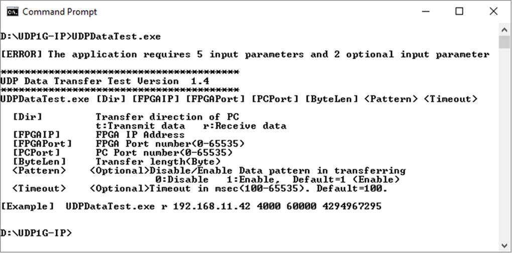
Figure 4‑1 udpdatatest application parameter
�udpdatatest� is an application on PC for sending or receiving UDP data. There are five parameters and two optional parameters. The input parameter should be matched to parameter setting on FPGA. More details of each input parameter are as follows.
1) Dir : t � when PC sends data to FPGA
r � when PC receives data from FPGA
2) FPGAIP : IP address setting on FPGA (default is 192.168.11.42)
3) FPGAPort : Port number of FPGA (default is 4000)
4) PCPort : PC port number for sending or receiving data
(default is 60001 for transferring data from PC to FPGA
or 60000 for transferring data from FPGA to PC)
5) ByteLen : Transfer length for sending or receiving in byte unit.
6) Pattern (optional): Default value when user does not input this parameter is 1.
0 � Generate dummy data in transmit mode or disable data verification
in receive mode.
1 � Generate incremental data in transmit mode or enable data
verification in receive mode.
7) Timeout (optional): Timeout of receiving data in milli seconds unit.
Default value when user does not input this parameter is 100.
Receive data mode
The step when running the test application in receive mode is described as follows.
1) Get parameters from user and verify that the input is valid.
2) Create the socket and then set properties of received buffer.
3) Set IP address and port number from user parameter and then connect.
4) Repeat to read data until total data is equal to set value or no more data is received with timeout asserting. During reading data, the application prints total received data on the console every second.
a) When Pattern=1, the read data is verified by 32-bit incremental pattern which is increased every 4-byte received data.
b) When Pattern=0, the read data is not verified.
5) When the read loop is finished by timeout condition, �Timeout� message is displayed with total lost size and total received size.
6) After finishing the operation, the application displays performance as a test result.
Transmit data mode
The step when running the test application in transmit mode is described as follows.
1) Follow step (1)-(3) in Receive data mode.
2) Send data to the send buffer for sending out. During sending data, the application prints total sent data on the console every second.
a) When Pattern=1, the send buffer is filled by 32-bit incremental pattern.
b) When Pattern=0, the send buffer is not filled. Dummy data is applied in the test.
3) After finishing sending all data, the application displays performance with total data size as a test result.
5 Revision History
|
Revision |
Date |
Description |
|
1.0 |
2-Mar-17 |
Initial Release |
|
1.1 |
14-Aug-18 |
Update design to interface by JTAG UART |
|
1.2 |
6-Dec-19 |
Add Function list |
Copyright: 2017 Design Gateway Co,Ltd.