UDP1G-IP reference design manual
Rev1.1 7-Jul-23
1 Introduction
Comparing to TCP, UDP provides a procedure to send messages with a minimum of protocol mechanism, but the data cannot guarantee to arrive destination because of no handshaking dialogues. Similar to TCP, UDP provides checksums for data integrity, and port numbers for addressing different functions at the source and destination of the datagram.
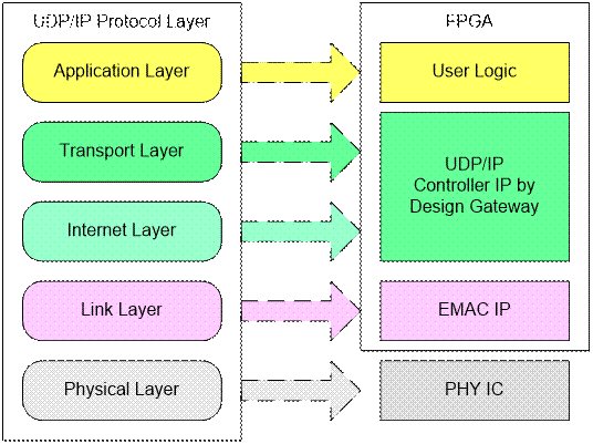
Figure 1‑1 UDP/IP Protocol Layer
UDP1G-IP implements Transport and Internet layer of UDP/IP Protocol. For transmit side, UDP1G-IP prepares UDP data from user logic and adds UDP/IP header to generate Ethernet packet format before sending out to EMAC. For receive side, UDP1G-IP validates UDP/IP header of the packet and extracts UDP data from the packet. Only UDP data of valid packet is stored to buffer for user logic reading.
The lower layer protocols are implemented by EMAC-IP from Xilinx and external PHY chip.
This reference design provides evaluation system which includes simple user logic to send and receive data by using UDP1G-IP. For user interface, CPU system is designed to interface with user through Serial console. The firmware is designed as bare-metal OS. Test application running on PC in the demo is “udp1gdatatest.exe”. The reference design is available on Xilinx development board to show high-speed transfer for both half-duplex and full-duplex mode. More details of the demo are described as follows.
2 Hardware overview
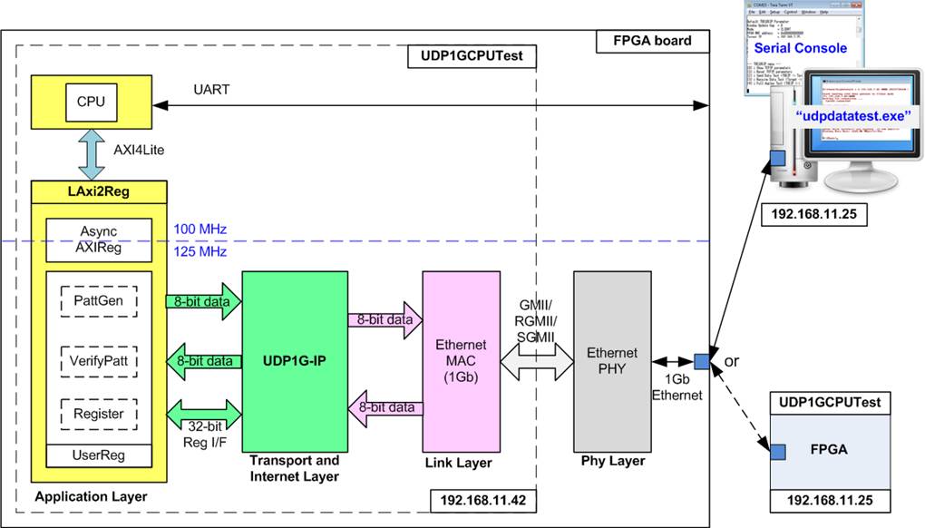
Figure 2‑1 Demo Block Diagram
In test environment, two devices are used for 1Gb Ethernet transferring. First device runs in client mode and another runs in server mode. To confirm UDP1G-IP operation in both modes, the demo can be tested by using two test environments. First environment uses two FPGAs (one is client and one is server). Second environment uses one FPGA and one PC, as shown in Figure 2‑1.
In FPGA logic, UDP1G-IP connects to Ethernet MAC and Ethernet PHY to complete all UDP/IP layer implementation. User interface of UDP1G-IP is connected to UserReg module within LAxi2Reg.
For user data interface, UserReg includes PattGen to generate test pattern to UDP1G-IP. Also, VerifyPatt is designed to verify received data from UDP1G-IP. Test pattern in the reference design is 32-bit increment data.
For user control interface, there are registers in UserReg to store test parameters from user such as transfer length and transfer direction. Input parameters are received from user through Serial console. CPU firmware validates all parameters from user before forwarding the set value to hardware through AXI4-Lite bus.
Due to the fact that CPU system and UDP1G-IP run in different clock domain, AsyncAXIReg module inside LAxi2Reg is designed as asynchronous circuit to support clock-crossing operation. Also, AsyncAXIReg converts AXI4-Lite bus signal which is standard bus in CPU system to be register interface.
In CPU system, two CPU peripherals are used, i.e. UART for user interface and Timer for measuring transfer performance. CPU detects LAxi2Reg module as CPU peripheral like Timer and UART.
“udp1gdatatest.exe” is the test application on PC applied in the demo. The application is designed to send or receive Ethernet data following UDP/IP protocol. To run as full-duplex test, two applications are called by using different port numbers (one for sending data and another for receiving data). In full-duplex mode, PattGen and VerifyPatt module inside UserReg transfer data with UDP1G-IP in both directions at the same time.
2.1 Ethernet PHY
Ethernet PHY is implemented by external PHY chip. The interface of external PHY chip must be matched to Ethernet MAC. Interface could be selected to be GMII, RGMII, SGMII, or 1000BASE-X. Ethernet speed is fixed to 1 Gbps mode.
2.2 Tri Mode Ethernet MAC
Xilinx provides Ethernet MAC IPs for running 1Gb Ethernet speed. Physical interface of Tri Mode Ethernet MAC IP could be selected to be GMII, RGMII, or internal interface. Internal interface is selected when physical interface is SGMII or 1000BASE-X. Also, 1G/2.5G Ethernet PCS/PMA is applied to interface with SGMII or 1000BASE-X interface. More details of the IP are described in following link.
Tri mode Ethernet MAC
https://www.xilinx.com/products/intellectual-property/temac.html
1G/2.5G Ethernet PCS/PMA
https://www.xilinx.com/products/intellectual-property/do-di-gmiito1gbsxpcs.html
Data interface of Ethernet MAC is designed by 8-bit AXI4 stream which could be connected to UDP1G-IP directly.
2.3 UDP1G-IP
UDP1G-IP implements UDP/IP stack and offload engine. Control and status signals for user interface are accessed through register interface. Data interface is accessed through FIFO interface. More details are described in datasheet.
https://dgway.com/products/IP/UDP-IP/dg_udp1gip_data_sheet_xilinx_en.pdf
2.4 LAxi2Reg
The hardware is connected to CPU through AXI4-Lite bus, similar to other CPU peripherals. The hardware registers are mapped to CPU memory address, as shown in Table 2‑1. The control and status registers for CPU access are designed in LAxi2Reg.
LAxi2Reg connects to UDP1G-IP for both data path and control path. As shown in Figure 2‑2, there are two clock domains applied in this block, i.e. 100 MHz (CpuClk) which is used to interface with CPU through AXI4-Lite bus and 125 MHz (MacTxClk) which is user clock domain for UDP1G-IP and EMAC.
AsyncAxiReg includes asynchronous circuit between 100 MHz and 125 MHz. More details of each hardware are described as follows.

Figure 2‑2 LAxi2Reg block diagram
2.4.1 AsyncAxiReg
This module is designed to convert signal interface of AXI4-Lite to be register interface. Also, it supports to convert clock domain from 100 MHz to be 125 MHz. Timing diagram of register interface is shown in Figure 2‑3.
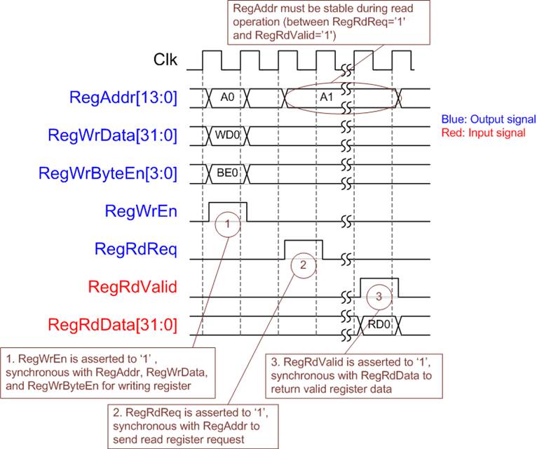
Figure 2‑3 Register interface timing diagram
To write register, timing diagram is same as RAM interface. RegWrEn is asserted to ‘1’ with the valid signal of RegAddr (Register address in 32-bit unit), RegWrData (write data of the register), and RegWrByteEn (the byte enable of this access: bit[0] is write enable for RegWrData[7:0], bit[1] is used for RegWrData[15:8], …, and bit[3] is used for RegWrData[31:24]).
To read register, AsyncAxiReg asserts RegRdReq=’1’ with the valid value of RegAddr (the register address in 32-bit unit). After that, the module waits until RegRdValid is asserted to ‘1’ to get the read data through RegRdData signal. During read access, RegAddr holds the same value until RegRdValid is asserted to ‘1’.
2.4.2 UserReg

Figure 2‑4 UserReg block diagram
Memory map of control and status signals inside UserReg module is shown in Table 2‑1.
0x0000 – 0x00FF is mapped to registers inside UDP1G-IP.
0x1000 – 0x10FF is mapped to registers inside UserReg (to control Tx Pattern Generator and Rx Data Verification).
To request write register, UserRegWrEn is asserted to ‘1’ with the valid of UserRegAddr. The upper bits of UserRegAddr are used to decode that CPU accesses UDP1G-IP area or internal register area. If CPU accesses UDP1G-IP area, UDPRegWrEn will be asserted to ‘1’. Otherwise, UserRegWrData is loaded to internal register which has matched lower bits of UserRegAddr. For example, rSetTxSize is loaded by UserRegWrData when UserRegAddr=0x1000. UserRegWrByteEn signal is not used in this module, so CPU firmware needs to access the hardware register by using 32-bit pointer only.
For read request, UserRegRdReq is asserted to ‘1’. RdDataMux selects status signals from internal register or UDP1G-IP, following the upper bits of UserRegAddr. In the next clock, the output of RdDataMux is forwarded to UserRegRdData. To synchronous with UserRegRdData, RegRdValid is designed by using one D Flip-flop, input by RegRdReq signal.
The upper logic in blue color of Figure 2‑4 is designed to generate test data to UDP1G-IP. rTxTrnEn is asserted to ‘1’ when write register address is 1004h. When rTxTrnEn is ‘1’, UDPTxFfWrEn is controlled by UDPTxFfFull. UDPTxFfWrEn is de-asserted to ‘0’ when UDPTxFfFull is ‘1’. rTotalTxCnt is data counter to check total data sending to UDPTxFf interface. rTotalTxCnt is also used to generate 32-bit increment data to UDPTxFfWrData signal. rTxTrnEn is de-asserted to ‘0’ when total data has been transferred completely (total data is set by rSetTxSize).
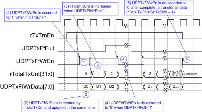
Figure 2‑5 Tx Pattern Generator Timing diagram
The logic in red color of Figure 2‑4 is designed to verify received data from UDP1G-IP. UDPRxFfRdEn is designed by using NOT logic of UDPRxFfRdEmpty. UDPRxFfRdData is valid in the next clock after asserting UDPRxFfRdEn to ‘1’. Read data with 1 clock latency (rUDPRxFfRdData) is compared to expected pattern (rExpPatt) when rFfRdEn[1]=’1’ (rFfRdEn[1] is UDPRxFfRdEn with two clock latency). rTotalRxCnt is data counter to check total read data from UDPRxFf. Similar to Tx path, expected pattern is 32-bit increment pattern. Fail flag (rFail) will be asserted to ‘1’ if Read Data is not equal to expected pattern.
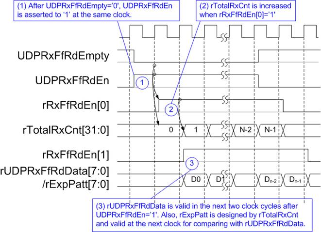
Figure 2‑6 Rx Data Verification Timing diagram
Table 2‑1 Register map Definition
|
Address |
Register Name |
Description |
|
Wr/Rd |
(Label in the “udp1gip_demo.c” ) |
|
|
BA+0x0000 – BA+0x00FF: UDP1G-IP Register Area More details of each register are described in Table3 of UDP1G-IP datasheet. |
||
|
BA+0x00 |
UDP_RST_REG |
Mapped to RST register within UDP1G-IP |
|
BA+0x04 |
UDP_CMD_REG |
Mapped to CMD register within UDP1G-IP |
|
BA+0x08 |
UDP_SML_REG |
Mapped to SML register within UDP1G-IP |
|
BA+0x0C |
UDP_SMH_REG |
Mapped to SMH register within UDP1G-IP |
|
BA+0x10 |
UDP_DIP_REG |
Mapped to DIP register within UDP1G-IP |
|
BA+0x14 |
UDP_SIP_REG |
Mapped to SIP register within UDP1G-IP |
|
BA+0x18 |
UDP_DPN_REG |
Mapped to DPN register within UDP1G-IP |
|
BA+0x1C |
UDP_SPN_REG |
Mapped to SPN register within UDP1G-IP |
|
BA+0x20 |
UDP_TDL_REG |
Mapped to TDL register within UDP1G-IP |
|
BA+0x24 |
UDP_TMO_REG |
Mapped to TMO register within UDP1G-IP |
|
BA+0x28 |
UDP_PKL_REG |
Mapped to PKL register within UDP1G-IP |
|
BA+0x38 |
UDP_SRV_REG |
Mapped to SRV register within UDP1G-IP |
|
BA+0x1000 – BA+0x10FF: UserReg control/status |
||
|
BA+0x1000 |
Total transmit length |
Wr [31:0] – Total transmitted size in byte unit. Valid from 1-0xFFFFFFFF. Rd [31:0] – Current transmitted size in byte unit (8-bit). The value is cleared to 0 when USER_CMD_REG is written by user. |
|
Wr/Rd |
(USER_TXLEN_REG) |
|
|
BA+0x1004 |
User Command |
Wr [0] – Start Transmit. Set ‘0’ to start transmit data from UserReg. [1] – Data Verification enable (‘0’: Disable data verification, ‘1’: Enable data verification) Rd [0] – UserReg busy from transmitting data (‘0’: Idle, ‘1’: Busy) [1] – Verification fail (‘0’: No error, ‘1’: Data verification is failed) |
|
Wr/Rd |
(USER_CMD_REG) |
|
|
BA+0x1008 |
User Reset |
Wr [0] – Reset signal. Set ‘1’ to reset the logic. This bit is auto-cleared to ‘0’. [8] – Set ‘1’ to clear TimerInt latch value Rd [8] – Latch value of TimerInt output from IP (‘0’: Normal, ‘1’: TimerInt=’1’ is detected) This flag can be cleared by system reset condition or setting USER_RST_REG[8]=’1’. |
|
Wr/Rd |
(USER_RST_REG) |
|
|
BA+0x100C |
FIFO status |
Rd [15:0]: Mapped to UDPRxFfRdCnt signal of UDP1G-IP [24]: Mapped to UDPTxFfFull signal of UDP1G-IP |
|
Rd |
(USER_FFSTS_REG) |
|
|
BA+0x1010 |
Total Receive length |
Rd [31:0] – Current received size in byte unit. The value is cleared to 0 when USER_CMD_REG is written by user. |
|
Rd |
(USER_RXLEN_REG) |
|
3 CPU Firmware Sequence
After FPGA boot-up, user must select the operation mode on FPGA to be client or server. The operation mode is the set value to UDP_SRV_REG register. In client mode, FPGA sends ARP request to get the MAC address from the destination device during initialization sequence. In server mode, FPGA waits ARP request from the destination device and returns ARP reply during initialization sequence.
To run the test by using two FPGAs, the operation mode on each FPGA must be different (one is client and another is server). In case of running FPGA with PC, it is recommended to set FPGA to client mode. It is easier to force PC to return ARP reply after receiving ARP request from FPGA, comparing to find the way to make PC sending ARP request to FPGA.
In the firmware, there are two sets of default parameters, i.e. client parameters and server parameters. The initialization sequence after system boot-up is as follows.
1) CPU receives the operation mode from user and displays default parameters on the console.
2) User inputs ‘x’ to complete initialization sequence by using default parameters or inputs other keys to change some parameters. In case of changing parameters, the operation sequence is same as Reset IP which is described in topic 3.2.
3) CPU waits until UDP1G-IP completes initialization sequence (UDP_CMD_REG[0]=’0’).
4) Main menu is displayed with five operations. More details of each operation are described as follows.
3.1 Show parameters
This menu is used to show current parameters of UDP1G-IP such as operation mode, source MAC address, destination IP address, source IP address, destination port, and source port. The sequence to display parameters is as follows.
1) Read network parameters from each variable in firmware.
2) Print out each variable.
3.2 Reset IP
This menu is used to change UDP1G-IP parameters such as IP address, source port number. After setting UDP1G-IP register, CPU resets the IP to re-initialize by using new parameters. CPU monitors busy flag to wait until the initialization is completed. The sequence of reset sequence is shown as follows.
1) Display current parameter value to the console.
2) Receive input parameters from user and check input value whether it is in a valid or not. If the input is invalid, the old value will be used instead of invalid input.
3) Force reset to UDP1G-IP by setting UDP_RST_REG[0]=’1’.
4) Set all parameters to UDP1G-IP register such as UDP_SML_REG, UDP_DIP_REG.
5) De-assert UDP1G-IP reset by setting UDP_RST_REG[0]=’0’.
6) Reset UserReg by sending reset to user logic (USER_RST_REG[0]=’1’).
7) Monitor UDP1G-IP busy flag (UDP_CMD_REG[0]). Wait until busy flag is de-asserted to ‘0’ to confirm that initialization sequence is completed.
3.3 Send data test
User needs to input two parameters, i.e. total transmit length and packet size. The operation will be cancelled if the input is invalid. During the test, 32-bit increment data is generated from the logic and sent to the target (PC or FPGA). The target verifies the received data by test application when running with PC or by verification module when running with FPGA. The operation is completed when total data are transferred from FPGA to PC/FPGA completely. The sequence of this test is as follows.
1) Receive transfer size and packet size from user and verify that all inputs are valid.
2) Set UserReg registers, i.e. transfer size (USER_TXLEN_REG), reset flag to clear initial value of test pattern (USER_RST_REG[0]=’1’), and command register to start data pattern generator (USER_CMD_REG=0). After that, test pattern generator in UserReg transmits data to UDP1G-IP.
3) Display recommended parameter of test application running on PC by reading current parameters in the system. Wait until user press any key to start IP sending operation.
4) Set parameters to UDP1G-IP to start operation, i.e. Packet size (UDP_PKL_REG), total size (UDP_TDL_REG), and Send command (UDP_CMD_REG=1).
5) Wait until operation is completed by monitoring busy flag (UDP_CMD_REG[0]=’0’). During monitoring busy flag, CPU reads current transfer size from user logic (USER_TXLEN_REG and USER_RXLEN_REG) and displays the results on the console every second.
6) Calculate performance and show test result on the console.
3.4 Receive data test
User sets total received size and data verification mode (enable or disable). The operation will be cancelled if the input is invalid. During the test, 32-bit increment data is generated to verify the received data from PC/FPGA when data verification mode is enabled. The sequence of this test is as follows.
1) Receive total transfer size and data verification mode from user. Verify that all inputs are valid.
2) Set UserReg registers, i.e. reset flag to clear initial value of test pattern (USER_RST_REG[0]=’1’) and data verification mode (USER_CMD_REG[1]=’0’ or ‘1’).
3) Display recommended parameter of test application to run on PC by reading current parameters in the system.
4) Wait until IP receives the first packet by monitoring current received size (USER_RXLEN_REG is not equal to 0). Start timer after receiving the first packet.
5) Wait until received size (USER_RXLEN_REG) does not change more than 1 sec or total data are received. During receiving data, CPU reads current transfer size from user logic (USER_TXLEN_REG and USER_RXLEN_REG) and displays the results on the console every second.
6) Stop timer. Check interrupt from timeout (USER_RST_REG[8]) and data verification flag (USER_CMD_REG[1]) register when verification mode is applied. Message will be displayed if some errors or interrupt are found.
7) Calculate performance and show test result on the console.
3.5 Full duplex test
This menu is designed to run full duplex test by transferring data between FPGA and PC/FPGA in both directions at the same time. Three inputs are received from user, i.e. total size for both directions, packet size for FPGA sending logic, and data verification mode for FPGA receiving logic.
To run full duplex test by using PC, user opens “udp1gdatatest” application on two consoles. First application is used to receive data with FPGA and another is used to send data with FPGA. The port using in two applications must be different.
When running full duplex test by using two FPGAs, one port is applied for both sending and receiving data. The sequence of this test is as follows.
1) Receive total data size, packet size, and data verification mode from user and verify that all inputs are valid.
2) Set UserReg registers, i.e. transfer size (USER_TXLEN_REG), reset flag to clear initial value of test pattern (USER_RST_REG[0]=’1’), and command register to start data pattern generator with data verification mode (USER_CMD_REG=1 or 3).
3) Display recommended parameter of test application running on PC by reading current parameters in the system.
4) Set UDP1G-IP registers, i.e. packet size (UDP_PKL_REG), total transfer size (UDP_TDL_REG), and write command (UDP_CMD_REG=1). IP starts sending data operation after UDP_CMD_REG is set to 1. For receiving data, IP is always ready to receive data without additional setting.
5) Wait until operation is completed for both sending and receiving direction.
a. For sending direction, wait until busy flag of UDP1G-IP (UDP_CMD_REG[0]) is equal to ’0’.
b. For receiving direction, wait until total received size is equal to set value or total received size does not change for one second (timeout condition)
During waiting, CPU reads current transfer size of both directions from user logic (USER_TXLEN_REG and USER_RXLEN_REG) and displays on the console every second.
6) Check interrupt from timeout (USER_RST_REG[8]) and data verification flag (USER_CMD_REG[1]) register when verification mode is applied. Message will be displayed if some errors or interrupt are found.
7) Calculate performance and show test result on the console.
4 Test Software description
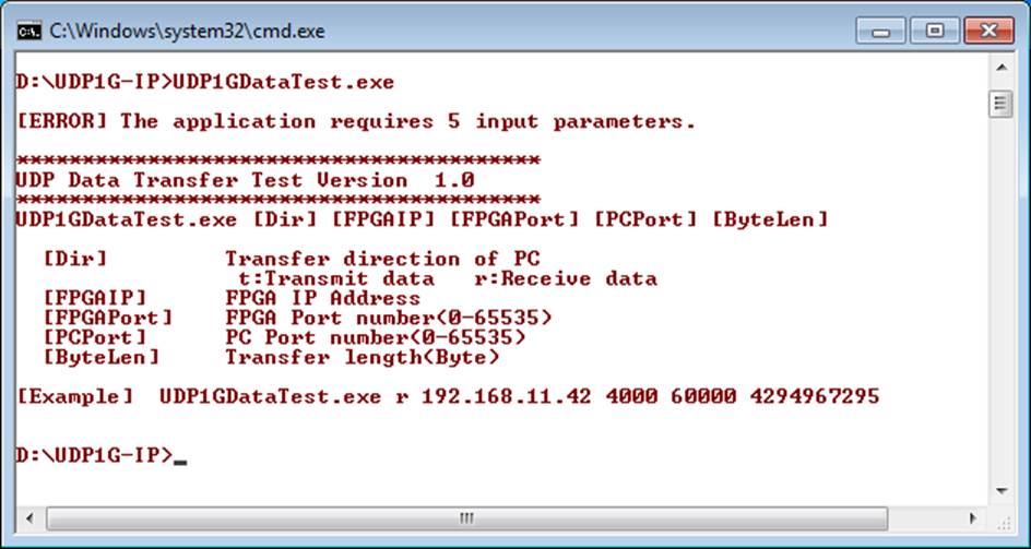
Figure 4‑1 udp1gdatatest application parameter
“udp1gdatatest” is an application on PC for sending or receiving UDP data. There are five parameters. The parameter input should be matched to parameter setting on FPGA. More details of each parameter input are followed.
1) Dir: t – when PC sends data to FPGA
r – when PC receives data from FPGA
2) FPGAIP : IP address setting on FPGA (default is 192.168.11.42)
3) FPGAPort : Port number of FPGA (default is 4000)
4) PCPort : PC port number for sending or receiving data
(default is 60001 for transferring data from PC to FPGA
or 60000 for transferring data from FPGA to PC)
5) ByteLen : Transfer length for sending or receiving in byte unit.
4.1 Receive data mode
The operation sequence of the application is as follows.
(1) Get parameters from user.
(2) Create socket and then set properties of receive buffer.
(3) Set IP address and port number from user inputs and then connect.
(4) Loop to verify data until total received data is equal to set value or no more received data within 1 sec. Verification pattern is 32-bit increment starting from 0. Pattern is increased after receiving 4 bytes. During running, application prints total received size on the console every second.
(5) In case of 1 sec timeout condition, “Timeout” message is displayed with total lost size and total receive size when end of operation.
4.2 Transmit data mode
The operation sequence of the application is as follows.
(1) – (3) are same as Receive data mode
(4) Generate 32-bit increment pattern to buffer and then send data out. The packet size is fixed to 1472 byte.
(5) After completing to send all data, the application displays performance with total data size as test result.
5 Revision History
|
Revision |
Date |
Description |
|
1.0 |
6-Jan-16 |
Initial Release |
|
1.1 |
20-Nov-18 |
Update user interface to be UART |
Copyright: 2016 Design Gateway Co,Ltd.