UDP10G IP reference design manual
3.6 Function list in User application
1 Introduction
Compared to the TCP protocol, the UDP protocol minimizes protocol mechanisms when sending data. There is no handshake and no data recovery process to confirm that the receiver accepts all data correctly. However, like TCP, UDP provides checksums for data integrity and port numbers for addressing different functions at the source and destination in networks.
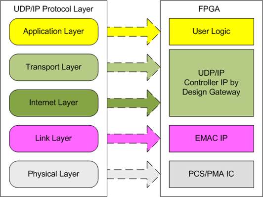
Figure 1‑1 UDP/IP Protocol Layer
The UDP10G-IP implements the Transport and Internet layers of the UDP/IP Protocol using fully hardwire logic, elimiating the need for a CPU or DDR. This choice allows user logic to focus on processing UDP payload data at the user interface of the UDP10G-IP.
The UDP10G-IP is responsible for constructing an Ethernet packet containing the UDP payload data from the user and transmitting it to the Ethernet MAC (EMAC). In cases where the user’s data size exceeds the maximum size of a single Ethernet packet, the UDP10G-IP will partition the data into multiple packets for transmission. Prior to transmission, the UDP10G-IP is also responsible for adding the UDP/IP header to each packet to form a complete Ethernet packet.
On the other hand, when the UDP10G-IP receives an Ethernet packet from the EMAC, it extracts and validates the packet. If the packet meets the criteria for validity, the UDP10G-IP extracts the UDP payload data from the packet and forwards it to the user logic. However, if the packet is found to be invalid, it is rejected.
The lower layer protocols are implemented by EMAC-IP and PCS/PMA-IP, where PCS/PMA-IP is provided by Intel FPGA while EMAC-IP can be implemented by DG 10GEMAC-IP or Intel FPGA EMAC-IP.
The reference design integrates three main components: a simple user logic module, the UDP10G-IP, and an Ethernet MAC, enabling data transfer through the UDP/IP protocol. This design facilitates data transfer between the host (FPGA) and the target, which can be a PC or another FPGA incorporating the UDP10G-IP.
For testing and validation, Design Gateway provides a test application named “udpdatatest” on the PC. This application is designed for the high-speed transmission or verification of UDP payload data over an Ethernet connection. Using a parameter to define data transfer direction, one application is called for one-way data transfer, while two applications are utilized for full-duplex test, allowing to send and receive data simultaneously.
To provide flexibility in testing, the user set the test parameters and control the operation of UDP10G-IP demo via JTAG UART, which is integrated with a CPU system The user can monitor the current status and set test parameters through the console. The CPU firmware is built using a simple bare-metal OS. More details of the demo are described below.
2 Hardware description

Figure 2‑1 Hardware architecture in reference design
In the test environment, two devices are used for data transfer over 10G Ethernet connection. The first device is an FPGA that configures its initialization mode as “Client”. In this mode, the FPGA is initialized by sending an ARP request packet to acquire the target MAC address. The other device can either be a PC or another FPGA, which is configured with the UDP10G-IP set to the initialization mode of “Server”. In this mode, it awaits the ARP request packet to obtain the target MAC addres). If a PC is used as the second device, the test application “udpdatatest” is provided to facilitate data transfer between the PC and the FPGA.
In the FPGA system, the UDP10G-IP connects with the 10G Ethernet MAC and 10G Ethernet PHY to implement all the TCP/IP layers. The user interface of the UDP10G-IP is connected to UserReg within Avl2Reg, which includes a Register file for interfacing with the Register interface, PattGen for sending test data via Tx FIFO interface, and PattVer for verifying test data via Rx FIFO interface. The Register file of UserReg is controlled by CPU firmware through the Avalon-MM bus.
Besides, the reference design includes additional logic components. MacRegCtrl is designed to configure control register through Avalon-MM interface when using the Intel FPGA 10G EMAC-IP. SFPConfig is designed to configure the SFP+ transceiver when running the demo on Cyclone10 GX board.
The test design uses two clock domains: CpuClk for the CPU system and MacTxClk for the user interface of EMAC and UDP10G-IP. Therefore, AsyncAvlReg is designed to support asynchronous signal transferring between CpuClk and MacTxClk. More information about each module inside the UDP10CPUTest is described below.
2.1 10GBASE-R PHY
The Intel 10GBASE-R PHY is applied to connect with 10G SFP+ module. The user interface of the PHY is connected to 10G Ethernet MAC through a 64-bit XGMII interface running at 156.25 MHz. Further details can be found in the following link.
On the Cyclone10 GX board, the ‘SFP_TX_Disable’ signal on SFP+ transceiver is configured using an I/O Expander. This I/O Expander is controlled via two-line I2C bus protocol. Therefore, the SFPConfig module is designed to serve as an I2C master, responsible for setting ‘SFP_TX_Disable’ to 0b on the SFP+ transceiver.
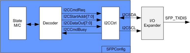
Figure 2‑2 SFPConfig block diagram
SFPConfig includes I2CCtrl, which acts as the I2C master controller, writing one-byte data to the register. In the I2CCtrl logic, the device number and clock divider are fixed values, and I2C clock (SCL) operates at 400 kHz. Within SFPConfig, a state machine configures two registers of the I/O expander: the configuration register (Addr=0x03) and the output port register (Addr=0x01). The default setting of ‘SFP_TXDIS’, assigned to P2, is set as the input port, but the design necessitates changing it to an output direction. Besides, the default output value of P2 output is 1b, but it needs to be changed to be 0b. In summary, the state machine operates in the following steps.
1) It sets the configuration register of the P2 port to an output direction by assigning I2CStartAddr=0x03 (configuration register) and I2CDataOut=0xFB (Bit2=0b for output direction).
2) It sets the output port register to 0xFB (data output at bit2=0b).
Once the register configuration is completed, the SFPConfig module transitions to the Idle state. Therefore, the configuration of P2 occurs once after the system is powered on. The timing diagram for the I2CCtrl user interface is shown in Figure 2‑3.
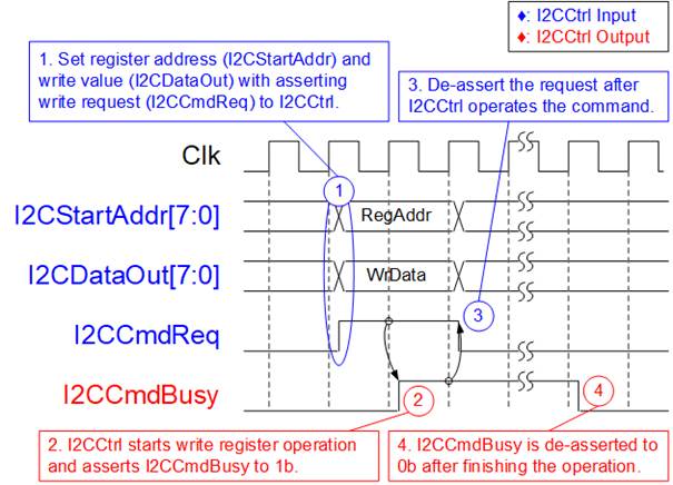
Figure 2‑3 Timing diagram of I2CCtrl
1) I2CCmdReq is set to 1b with valid values for I2CStartAddr and I2CDataOut. All inputs must remain unchanged until I2CCtrl asserts I2CCmdBusy to 1b.
2) I2CCmdBusy is set to 1b after I2CCtrl has loaded all input parameters and initiated the write register operation.
3) I2CCmdReq is set to 0b to clear the write request and prepares the parameters for the next operation.
4) Once I2CCtrl completes the operation, I2CCmdBusy is de-asserted to 0b.
2.2 10G EMAC
The 10G EMAC serves as the interface module between UDP10G-IP and the 10GBASE-R PHY. It employs a 64-bit Avalon stream interface with UDP10G-IP and a 64-bit XGMII interface running at 156.25 MHz with the 10GBASE-R PHY. Both DG 10G EMAC-IP and Intel FPGA 10G EMAC-IP can be used in the reference design. For more detailed information about the 10G EMAC IP, please refer to the following links.
DG 10G EMAC-IP
https://dgway.com/products/IP/10GEMAC-IP/dg_tengemacip_data_sheet_intel_en/
Intel FPGA 10G EMAC IP
When using the Intel FPGA 10G EMAC-IP, it is necessary to include MacRegCtrl to configure the 10G EMAC parameters through a 32-bit Avalon-MM bus interface. MacRegCtrl is designed as an Avalon-MM master for both writing and reading registers within the 10G EMAC IP. The details of the hardware inside MacRegCtrl are shown in Figure 2‑4.

Figure 2‑4 MacRegCtrl block diagram
A state machine is designed to execute register write/read operation in the following sequence.
1) Disable the transmit and receive paths of the EMAC.
2) Wait until both transmit and receive paths are idle.
3) Configure the receive module to remove CRC and padding.
4) Disable the transmission of pause frames.
5) Enable both the transmit and receive paths of the EMAC.
2.3 UDP10G IP
https://dgway.com/products/IP/UDP10G-IP/dg_udp10gip_data_sheet_intel_en/
2.4 CPU and Peripherals
The CPU system uses a 32-bit Avalon-MM bus as the interface to access peripherals such as the Timer and JTAG UART. The system also integrates an additional peripheral to access the test logic by assigning a unique base address and address range. To support CPU read and write operations, the hardware logic must comply with the Avalon-MM bus standard. Avl2Reg module, as shown in Figure 2‑5, is designed to connect the CPU system via the Avalon-MM interface, in compliance with the standard.

Figure 2‑5 Avl2Reg block diagram
Avl2Reg consists of AsyncAvlReg and UserReg. AsyncAvlReg converts Avalon-MM signals into a Register interface with a 32-bit data bus size, similar to Avalon-MM data bus size. It also includes asynchronous logic to handle clock domain crossing between the CpuClk and MacTxClk domain.
UserReg includes the Register file of the parameters and the status signals of test logics. Both the data interface and control interface of UDP10G-IP are connected to UserReg. More details of AsyncAvlReg and UserReg are described as follows.
2.4.1 AsyncAvlReg
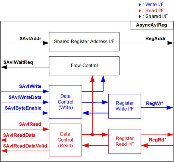
Figure 2‑6 AsyncAvlReg Interface
The Avalon-MM bus interface signal can be grouped into three categories: Write channel (blue), Read channel (red), and Shared control channel (black). More details about the Avalon-MM interface specification can be found in the following document.
https://www.intel.com/content/dam/www/programmable/us/en/pdfs/literature/manual/mnl_avalon_spec.pdf
According to Avalon-MM specification, only one command (write or read) can be executed at a time. AsyncAvlReg’s logic is divided into three groups: Write control logic, Read control logic, and Flow control logic. The flow control logic asserts SAvlWaitReq to hold the next request from the Avalon-MM interface if the current request has not finished. Write control and Write data I/F of the Avalon-MM bus are latched and transferred to the Write register interface with clock domain crossing registers. Similarly, Read control I/F are latched and transferred to be Read register interface. Afterward, the data returned from Register Read I/F is transferred to Avalon-MM bus with using clock domain crossing registers. The Address I/F of Avalon-MM is also latched and transferred to the Address register interface.
The Register interface is compatible with the single-port RAM interface for write transactions. However, the read transaction of the Register interface is slightly modified from RAM interface by adding RdReq and RdValid signals to control the read latency time. Since the address of the Register interface is shared for write and read transactions, the user cannot write and read the register at the same time. The timing diagram of the Register interface is shown in Figure 2‑7.
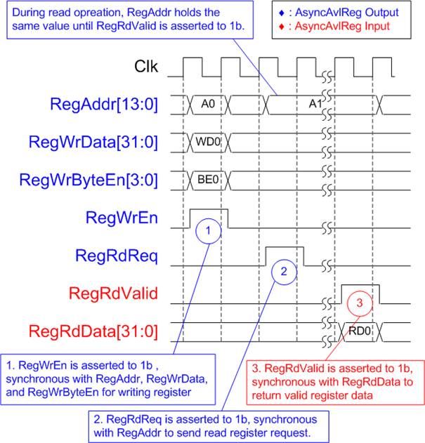
Figure 2‑7 Register interface timing diagram
1) Timing diagram to write register is similar to that of a single-port RAM. The RegWrEn signal is set to 1b, along with a valid RegAddr (Register address in 32-bit units), RegWrData (write data for the register), and RegWrByteEn (write byte enable). The byte enable consists of four bits that indicate the validity of the byte data. For example, bit[0], [1], [2], and [3] are set to 1b when RegWrData[7:0], [15:8], [23:16], and [31:24] are valid, respectively.
2) To read register, AsyncAvlReg sets the RegRdReq signal to 1b with a valid value for RegAddr. The 32-bit data is returned after the read request is received. The slave detects the RegRdReq signal being set to start the read transaction. In the read operation, the address value (RegAddr) remains unchanged until RegRdValid is set to 1b. The address can then be used to select the returned data using multiple layers of multiplexers.
3) The slave returns the read data on RegRdData bus by setting the RegRdValid signal to 1b. After that, AsyncAvlReg forwards the read value to the SAvlRead interface.
2.4.2 UserReg

Figure 2‑8 UserReg block diagram
Register Block
The address range, mapped to UserReg, is split into two areas: UDP10G-IP register (0x0000-0x00FF) and UserReg register (0x1000-0x10FF). The Address decoder decodes the upper bits of RegAddr to select the active hardware. Since the Register file inside UserReg is 32-bit bus size, Write byte enable (RegWrByteEn) is not used. To write hardware registers, the CPU must use a 32-bit pointer to place a 32-bit valid value on the write data bus.
For reading a register, a multiplexer selects the data to return to CPU by using the address. The lower bits of RegAddr are applied to select the active data within each Register area. While the upper bits are used to select the returned data from each Register area. The total latency time of read data is equal to one clock cycle, and RegRdValid is created by RegRdReq by asserting a D Flip-flop. More details of the address mapping within the UserReg module are shown in Table 2‑1.
Table 2‑1 Register map Definition
|
Address |
Register Name |
Description |
|
Wr/Rd |
(Label in the “udp10gtest.c”) |
|
|
BA+0x0000 – BA+0x00FF: UDP10G-IP Register Area More details of each register are described in UDP10G-IP datasheet. |
||
|
BA+0x0000 |
UDP_RST_INTREG |
Mapped to RST register within UDP10G-IP |
|
BA+0x0004 |
UDP_CMD_INTREG |
Mapped to CMD register within UDP10G-IP |
|
BA+0x0008 |
UDP_SML_INTREG |
Mapped to SML register within UDP10G-IP |
|
BA+0x000C |
UDP_SMH_INTREG |
Mapped to SMH register within UDP10G-IP |
|
BA+0x0010 |
UDP_DIP_INTREG |
Mapped to DIP register within UDP10G-IP |
|
BA+0x0014 |
UDP_SIP_INTREG |
Mapped to SIP register within UDP10G-IP |
|
BA+0x0018 |
UDP_DPN_INTREG |
Mapped to DPN register within UDP10G-IP |
|
BA+0x001C |
UDP_SPN_INTREG |
Mapped to SPN register within UDP10G-IP |
|
BA+0x0020 |
UDP_TDL_INTREG |
Mapped to TDL register within UDP10G-IP |
|
BA+0x0024 |
UDP_TMO_INTREG |
Mapped to TMO register within UDP10G-IP |
|
BA+0x0028 |
UDP_PKL_INTREG |
Mapped to PKL register within UDP10G-IP |
|
BA+0x0038 |
UDP_SRV_INTREG |
Mapped to SRV register within UDP10G-IP |
|
BA+0x003C |
UDP_VER_INTREG |
Mapped to VER register within UDP10G-IP |
|
BA+0x1000 – BA+0x10FF: UserReg control/status |
||
|
BA+0x1000 |
Total transmit length |
Wr [31:0] – Total transmitted size in QWord unit (64-bit). Valid from 1-0xFFFFFFFF. Rd [31:0] – Current transmitted size in QWord unit (64-bit). The value is cleared to 0 when USER_CMD_INTREG is written by user. |
|
Wr/Rd |
(USER_TXLEN_INTREG) |
|
|
BA+0x1004 |
User Command |
Wr [0] – Start Transmitting. Set 0b to start transmitting. [1] – Data Verification enable (0b: Disable data verification, 1b: Enable data verification) Rd [0] – PattGen Busy. (0b: Idle, 1b: PattGen is busy) [1] – Data verification error (0b: Normal, 1b: Error) This bit is auto-cleared when user starts new operation or reset. |
|
Wr/Rd |
(USER_CMD_INTREG) |
|
|
BA+0x1008 |
User Reset |
Wr [0] – Reset signal. Set 1b to reset the logic. This bit is auto-cleared to 0b. [8] – Set 1b to clear read value of IntOut latched value Rd [8] – Latched value of IntOut, the output from IP (0b: Normal, 1b: IntOut has been asserted to 1b) This flag can be cleared by system reset condition or setting USER_RST_INTREG[8]=1b. [16] – Ethernet Linkup status (0b: Link down, 1b: Link up) |
|
Wr/Rd |
(USER_RST_INTREG) |
|
|
BA+0x100C |
FIFO status |
Rd [2:0]: Mapped to UDPRxFfLastRdCnt signal of UDP10G-IP [15:3]: Mapped to UDPRxFfRdCnt signal of UDP10G-IP [24]: Mapped to UDPTxFfFull signal of UDP10G-IP |
|
Rd |
(USER_FFSTS_INTREG) |
|
|
BA+0x1010 |
Total receive length |
Rd [31:0] – Current received size from UDP10G-IP in QWord unit (64-bit). The value is cleared to 0 when USER_CMD_INTREG is written by user. |
|
Rd |
(USER_RXLEN_INTREG) |
|
|
BA+0x1080 |
EMAC IP version |
Rd[31:0] – Mapped to IPVersion output from DG 10GEMAC-IP when the system integrates DG 10GEMAC-IP. |
|
Rd |
(EMAC_VER_INTREG) |
|
Pattern Generator
The logic diagram and timing diagram of Pattern Generator (PattGen) are illustrated in Figure 2‑9 and Figure 2‑10, respectively.

Figure 2‑9 PattGen block
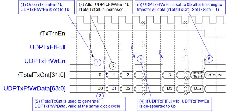
Figure 2‑10 PattGen Timing diagram
When USER_CMD_INTREG[0] is set to 0b, PattGen initiates the operation of generating test data by setting rTxTrnEn to 1b. While rTxTrnEn remains set to 1b, UDPTxFfWrEn is controlled by UDPTxFfFull. If UDPTxFfFull is 1b, UDPTxFfWrEn is de-asserted to 0b. The data counter, rTotalTxCnt, checks the total amount of data sent to UDP10G-IP. The lower bits of rTotalTxCnt generate 32-bit incremental data for the UDPTxFfWrData signal. Once all data has been transferred, equal to rSetTxSize, rTxTrnEn is de-asserted to 0b.
Pattern Verification
The logic diagram and timing diagram of Pattern Verification (PattVer) are illustrated in Figure 2‑11 and Figure 2‑12, respectively. The verification feature is executed when the verification flag (rVerifyEn) is enabled.
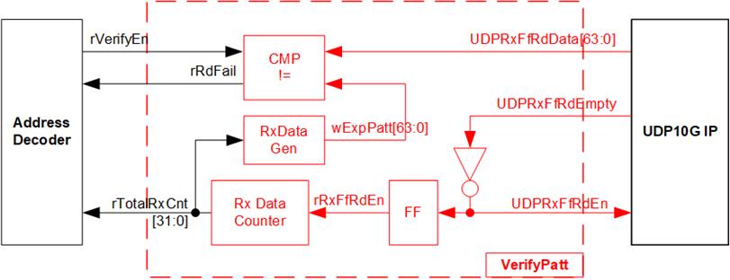
Figure 2‑11 PattVer block
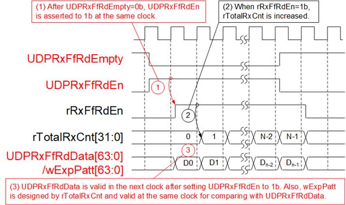
Figure 2‑12 PattVer Timing diagram
When rVerifyEn is set to 1b, the verification logic is processed. It compares the received data (UDPRxFfRdData) with the expected data (wExpPatt). If comparison fails, rRdFail is asserted to 1b. The UDPRxFfRdEn signal is created by applying NOT logic to UDPRxFfRdEmpty. The data for comparison, UDPRxFfRdData, becomes valid in the next clock cycle. To count the total size of received data, rTotalRxCnt is enabled by rRxFfRdEn, which is delayed by one clock cycle from UDPRxFfRdEn. The lower bits of rTotalRxCnt are applied to generate wExpPatt for comparison with UDPRxFfRdData. Therefore, UDPRxFfRdData and wExpPatt are valid in the same clock cycle and can be compared using rRxFfRdEn signal.
3 CPU Firmware on FPGA
Upon FPGA boot-up, a welcome message is presented. The status of the Ethernet link (USER_RST_REG[16]) is continuously monitored until it is established. Following this, the user is prompts to select the initialization mode for UDP10G-IP, choosing between Client or Server mode.
For initialization in Client mode, UDP10G-IP sends an ARP request packet to obtain the MAC address from the target device. In Server mode, UDP10G-IP awaits an ARP request packet to decode the MAC address and subsequently responds with an ARP reply packet to complete the initialization process.
In scenarios involving two FPGA boards within the test environment, it is crucial that the initialization mode differs between the two UDP10G-IPs, with one functioning as a Client and the other as a Server. However, if the target device is a PC, rather than an FPGA with integrated UDP10G-IP, it is recommended to set the UDP10G-IP to Client mode.
The CPU firmware on UDP10G-IP demo incorporates two default parameters for each initialization mode. Figure 3‑1 provides an example of the initialization sequence following system boot-up.
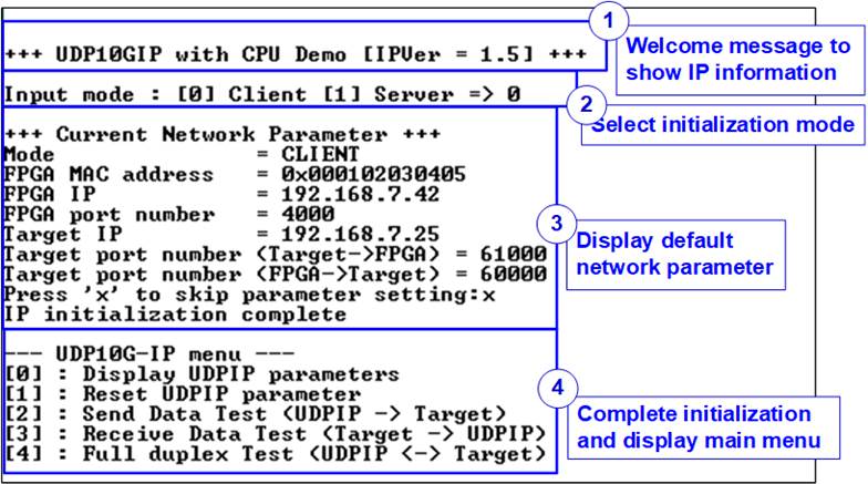
Figure 3‑1 System initialization in Client mode by using default parameters
The initialization sequence comprises four steps.
1) Upon FPGA boot-up, the CPU polls the status of the Ethernet link (USER_RST_INTREG[16]). The CPU waits until the link is up, and then displays a welcome message to show IP information.
2) The menu to select the initialization mode of UDP10G-IP is displayed, allowing the user to choose the Client or Server mode
3) The CPU displays the default values of the network parameters. The details of how to change the parameter are provided in Reset parameters menu (refer to section 3.2).
4) The CPU waits until the IP completes the initialization process by checking if busy status (UDP_CMD_INTREG[0]) is equal to 0b. After that, “IP initialization complete” is displayed with the main menu. There are five test operations in the main menu, and more details of each menu are described below.
3.1 Display parameters
This menu displays the current values of all UDP10G-IP parameters. The following steps are executed to display parameters.
1) Check the initialization mode.
2) Read all network parameters from each variable in the firmware following the initialization mode, including Source MAC address, Source IP address, Source port number, Target IP address, and Target port number.
Note: The Source parameters are the settings of the host FPGA integrated with the UDP10G-IP, while the Target parameters refer to the settings of a connected PC or another FPGA.
3) Print out each variable.
3.2 Reset IP
This menu is used to change some UDP10G-IP parameters, such as IP address and source port number. After setting the updated values to UDP10G-IP, the CPU resets to re-initialize the IP using new parameters. Finally, the CPU waits until the initialization is completed. The following steps are executed to reset the parameters.
1) Display all parameters on the console, similar to section 3.1 (Display parameters).
i) Receive the initialization mode from the user. If the initialization mode is changed, display the latest parameter set of new mode on the console.
3) Force reset to PattGen and PattVer logic by setting USER_RST_INTREG[0]=1b.
4) Force reset to UDP10G-IP by setting UDP_RST_INTREG[0]=1b.
5) Set the parameter values to UDP10G-IP registers, such as UDP_SML_INTREG and UDP_DIP_INTREG.
6) De-assert UDP10G-IP reset by setting UDP_RST_INTREG[0]=0b to initiate the initialization process.
7) Monitor the UDP10G-IP busy flag (UDP_CMD_INTREG[0]) until the initialization process is finished (IP busy flag is de-asserted to 0b).
3.3 Send data test
The following are the steps to send data.
1) Receive the transfer size and packet size from the user and verify that all inputs are valid. If any input is invalid, the operation is cancelled.
2) Configure the UserReg registers, including the transfer size (USER_TXLEN_INTREG), the Reset flag to clear the initial value of test pattern value (USER_RST_INTREG[0]=1b), and the Command register to start the Data pattern generator (USER_CMD_INTREG=0). After that, the Test pattern generator within UserReg starts generating test data to UDP10G-IP.
4) Upon receiving any key pressed, configure the parameters of UDP10G-IP for initiating the operation. Set the packet size to UDP_PKL_INTREG, the total size to UDP_TDL_INTREG, and set UDP_CMD_INTREG to 1b to start sending data.
5) Monitor the completion of the operation by observing the busy flag of the UDP10G-IP (UDP_CMD_INTREG[0]=0b). While monitoring the IP busy flag, the CPU periodically reads the current transfer size from the user logic (USER_TXLEN_INTREG) and displays it on the console every second.
6) Once the operation is completed, the CPU calculates the performance and displays the test result on the console.
3.4 Receive data test
This menu allows the user to execute Receive data test. The user can set the parameters such as total receive length. If all inputs are valid, a 32-bit incremental test data is created for verification with the received data from either PC or FPGA when the data verification is enabled.
The following are the steps to receive data.
1) Receive the total transfer size and data verification mode from the user and verify that all inputs are valid. If any input is invalid, the operation is cancelled.
2) Configure the UserReg registers as follows.
i) Set the Reset flag to clear the initial value of the test pattern
(USER_RST_INTREG[0]=1b)
ii) Set Data verification mode (USER_CMD_INTREG[1]=0b to only read the received data, or 1b to read and verify the received data).
3) Display recommended parameter (similar to Step 3 of Send data test).
4) Wait until the total number of received data (USER_RXLEN_INTREG) reaches the specified value (completion condition), or if there is no update in the received data count for 100 msec (timeout condition). While receiving data, the CPU will periodically display the current number of received data on the console every second.
5) Stop the timer and check for interrupt from the timeout (USER_RST_INTREG[8]) and data verification flag (USER_CMD_INTREG[1]) registers when the verification mode is active. If any errors are detected, an error message will be displayed.
6) Calculate the performance and display the test result on the console.
3.5 Full duplex test
This menu enables full duplex testing by simultaneously transferring data between the FPGA and another device (PC/FPGA) in both directions. User-defined parameters, such as the total transfer length, are received to initiate the test. If all inputs are valid, the data transfer begins and completes when the data is completely transferred in both directions.
Note: When testing with a PC, the transfer size on the test application (udpdatatest) must match the transfer size set on the FPGA. Two “udpdatatest” applications are executed, one for sending data and another for receiving data using different port number. When testing with two FPGAs, the port number for sending and receiving data are identical.
The steps to execute a full duplex test are as follows.
2) Set UserReg registers, including transfer size (USER_TXLEN_INTREG), the Reset flag to clear the initial value of the test pattern (USER_RST_INTREG[0]=1b), and the Command register to start Data pattern generator with data verification mode (USER_CMD_INTREG=0 or 2).
3) Display the recommended parameters for the test application that runs on the PC from the current system parameters.
4) Set UDP10G-IP registers, including packet size (UDP_PKL_INTREG), total transfer size (UDP_TDL_INTREG), and Send command (UDP_CMD_INTREG=1). The IP begins sending data once the UDP_CMD_INTREG is set to 1b. For receiving data, the IP is always ready to receive data without any additional setting.
5) The CPU controls data flow of both directions simultaneously, involving two concurrent tasks.
a) For sending data, the CPU continuously monitors the IP busy flag
(UDP_CMD_INTREG[0]) and waits until it is de-asserted to 0b. The IP busy flag becomes de-asserted when the Send command is finished.
b) For receiving data, the CPU tracks the total number of received data. The read process finishes when the total number of received data matches the expected value (no data loss). In the event that the total number of received remains unchanged for 100 msec (timeout), the read process is also finished.
While the data is not completely transferred, the current sizes of transmitted data (USER_TXLEN_INTREG) and received data (USER_RXLEN_INTREG) are read and displayed on the console every second.
7) Calculate performance and display the test result on the console.
3.6 Function list in User application
This topic describes the function list to run UDP10G-IP operation.
|
void init_param(void) |
|
|
Parameters |
None |
|
Return value |
None |
|
Description |
Reset parameter Reset parameters following the description in section 3.2. In this function, the ‘show_param’ and ‘input_param’ functions are called to display parameters and get parameters from user. |
|
int input_param(void) |
|
|
Parameters |
None |
|
Return value |
0: Valid input, -1: Invalid input |
|
Description |
Receive network parameters from user, i.e., the initialization mode, FPGA MAC address, FPGA IP address, FPGA port number, Target IP address, and Target port numbers. Each input is validated separately. It will be updated when the input is valid. If it is invalid, that particular parameter will not be updated. After receiving all parameters, calling ‘show_param’ function to display parameters. |
|
void show_cursize(void) |
|
|
Parameters |
None |
|
Return value |
None |
|
Description |
To display the amount of data transmitted and received on the console, first read the USER_TXLEN_INTREG and USER_RXLEN_INTREG to obtain the current values. Then, convert the values to appropriate units, i.e., bytes, Kbytes, or Mbytes and display them on the console. |
|
void show_interrupt(void) |
|
|
Parameters |
None |
|
Return value |
None |
|
Description |
Read interrupt status from UDP_TMO_INTREG and decode interrupt type to display the details of interrupt on the console. |
|
void show_param(void) |
|
|
Parameters |
None |
|
Return value |
None |
|
Description |
Display the parameters following the description in section 3.1. |
|
void show_result(void) |
|
|
Parameters |
None |
|
Return value |
None |
|
Description |
To display the total amount of data transmitted and received, first read USER_TXLEN_INTREG and USER_RXLEN_INTREG registers. Next, read the global parameters, timer_val and timer_upper_val, to calculate the total time usage in usec, msec, or sec units. Finally, calculate the transfer performance and display it in MB/s. |
|
int udp_recv_test(void) |
|
|
Parameters |
None |
|
Return value |
0: The operation is successful -1: Receive invalid input or error is found |
|
Description |
Run Receive data test following description in section 3.4. If timeout is triggered, it calls ‘show_interrupt’ function. Also, it calls ‘show_cursize’, and ‘show_result’ functions to update the progress and the results of the operation. |
|
int udp_send_test(void) |
|
|
Parameters |
None |
|
Return value |
0: The operation is successful -1: Receive invalid input or error is found |
|
Description |
Run Send data test following description in section 3.3. It calls ‘show_cursize’ and ‘show_result’ functions to update the progress and the results of the operation. |
|
int udp_txrx_test(void) |
|
|
Parameters |
None |
|
Return value |
0: The operation is successful -1: Receive invalid input or error is found |
|
Description |
Run Full duplex test following described in section 3.5. If timeout is triggered, it calls ‘show_interrupt’ function. Also, it calls ‘show_cursize’, and ‘show_result’ functions to update the progress and the results of the operation. |
|
void wait_ethlink(void) |
|
|
Parameters |
None |
|
Return value |
None |
|
Description |
Read USER_RST_INTREG[16] and wait until the Ethernet connection is linked up |
4 Test Software on PC
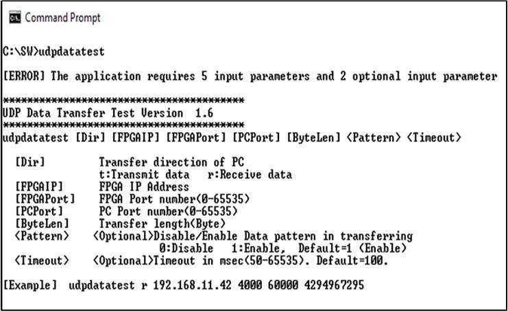
Figure 4‑1 udpdatatest application parameter
The “udpdatatest” application is executed to send or receive UDP data on a PC. It requires five mandatory parameters and two optional parameters. It is important to ensure that the parameter inputs match the parameters set on the FPGA. The details of each parameter input are as follows.
1) Dir: : t – when PC sends data to FPGA
: r – when PC receives data from FPGA
2) FPGAIP : IP address setting for FPGA (Default value is 192.168.7.42)
3) FPGAPort : Port number for FPGA (Default value is 4000)
4) PCPort : PC port number for sending or receiving data
(Default is 60001 for PC to FPGA and 60000 for FPGA to PC)
5) ByteLen : Transfer length for sending or receiving in byte unit. This value must be
aligned to 8 from UDP10G-IP limitation.
1) Pattern : Default value when user does not input this parameter is 1.
0 – Generate dummy data in transmit mode or disable data verification
in receive mode.
1 – Generate incremental data in transmit mode or enable data verification in receive mode.
2) Timeout : Timeout for receiving data in msec unit.
Default value when user does not input this parameter is 100.
The 100 ms is recommended value for running with UDP10G-IP.
Transmit data mode
The steps for running the test application in transmit mode are as follows.
1) Get the parameters from the user and verify that all inputs are valid.
2) Create a socket and configure the Receive buffer properties.
3) Set the IP address and port number based on the user parameters, and then establish a connection.
4) Populate the Send buffer with data for transmission. While the data is being sent, the application prints the total amount of data sent every second to the console.
a) If Pattern=1, the Send buffer is filled with a 32-bit incremental pattern.
b) If Pattern=0, the Send buffer is not filled and dummy data is used for the test.
5) After all data has been sent, the application displays the test results, including the total size of transmitted data and the performance.
Receive data mode
The steps when running the test application in receive mode are as follows.
1) Follow step (1)-(3) from the Transmit data mode.
2) Continuously read data until the total number of received data equals the set value. If there is no new data received before the timeout, the operation is cancelled. During the data reception, the application prints the total amount of received data every second.
a) If Pattern=1, the received data is verified using a 32-bit incremental pattern that increases every four bytes of received data.
b) If Pattern=0, the received data is not verified.
3) If the read loop finishes due to a timeout, the application displays a “Timeout” message with the total number of lost data and received data. The total time used is also reduced by timeout value.
4) After the operation is completed, the application displays the test results, including the performance and the total amount of received data.
5 Revision History
|
Revision |
Date |
Description |
|
1.4 |
18-Oct-23 |
Update udpdatatest features |
|
1.3 |
23-May-19 |
Support FPGA <-> FPGA connection |
|
1.2 |
22-Mar-18 |
Add Avl2Reg details |
|
1.1 |
17-Nov-17 |
Correct Receive data test sequence |
|
1.0 |
14-Sep-17 |
Initial Release |
Copyright: 2017 Design Gateway Co,Ltd.