Rev1.0 12-Jul-23
2.2 XXVGMacIFTx (only when using 25G Ethernet IP for Agilex)
2.3 XXVGMacIFRx (only when using 25G Ethernet IP for Agilex)
3.6 Function list in User application
1 Introduction
Comparing to TCP protocol, UDP protocol provides a procedure to send data with a minimum of protocol mechanism. There is no handshake and no data recovery process for the sender to confirm that the receiver accepts all data correctly. Similar to TCP protocol, UDP protocol provides checksum for data integrity and port numbers for addressing different functions at the source and the destination in the networks.
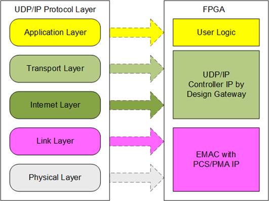
Figure 1‑1 UDP/IP protocol layer
UDP25G-IP implements Transport and Internet layer of UDP/IP Protocol for building Ethernet packet from the user data (UDP payload data) to EMAC. UDP25G-IP splits the user data to a packet size and then inserts UDP/IP header. On the other hand, the received Ethernet packet from EMAC is extracted by UDP25G-IP. The header of the packet is verified and UDP payload data is forwarded to the user logic when the packet is valid. Otherwise, the packet is rejected.
The lower layer protocols are implemented by 25G Ethernet IP, including EMAC and PCS/PMA logic. The reference design uses 25G Ethernet IP, provided by Intel FPGA.
The reference design provides the evaluation system which includes simple user logic to transfer data by using UDP25G-IP. In the reference design, the target device for transferring UDP payload data with UDP25G-IP is Test PC or another UDP25G-IP on FPGA board. When running with PC, the test application for transferring UDP payload data via Ethernet connection, udpdatatest, must run.
To allow the user controlling the test parameters and the operation of UDP25G-IP demo via JTAG UART, the CPU system is included. It is easy for the user to set the test parameters and monitor the current status on the console. The firmware on CPU is built by using bare-metal OS. More details of the demo are described as follows.
2 Hardware overview
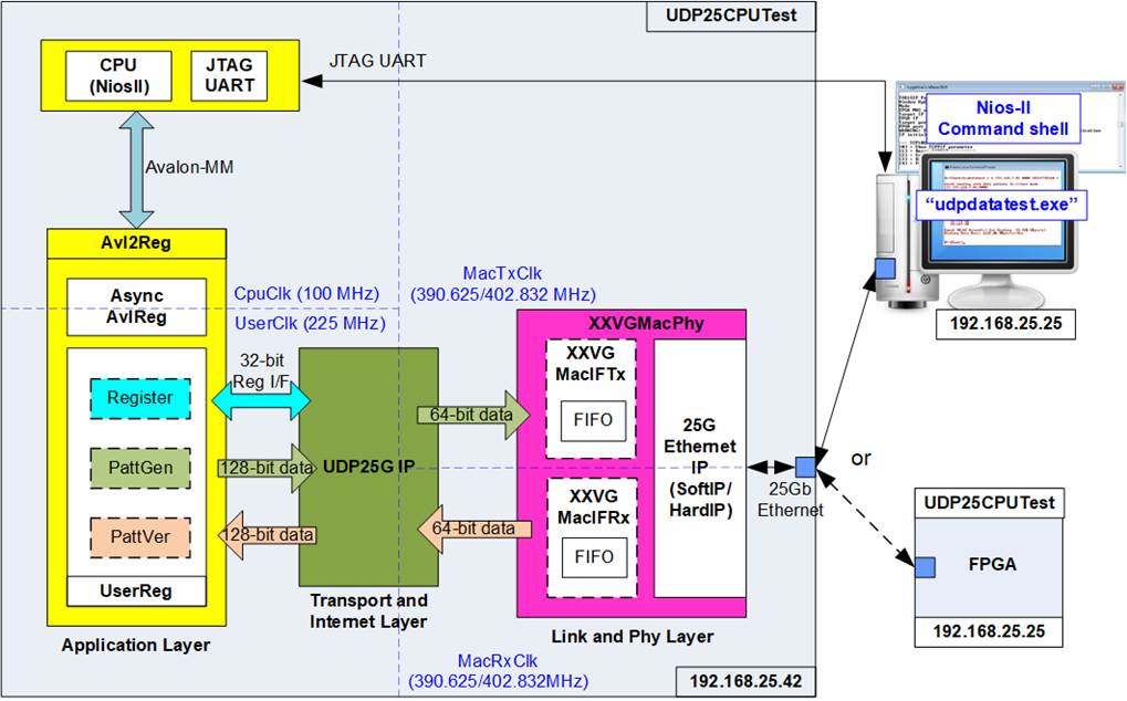
Figure 2‑1 Demo block diagram
In test environment, two devices are used for 25Gb Ethernet transferring. First device is UDP25G-IP which may be initialized by Client or Fixed-MAC mode. The second device may be Test PC which runs udpdatatest or another FPGA including UDP25G-IP that is initialized by Server or Fixed-MAC mode.
In FPGA system, UDP25G-IP connects with 25G Ethernet MAC and PHY (XXVGMacPhy) to complete all UDP/IP layer implementation. User interface of UDP25G-IP connects to UserReg within Avl2Reg which consists of Register file for control signals by Register interface, PattGen for sending test data via Tx FIFO interface, and PattVer for verifying test data via Rx FIFO interface. Register files of UserReg are controlled by CPU firmware through Avalon-MM bus.
25G Ethernet MAC and PHY can be implemented by two ways, depending on 25G Ethernet IP characteristic. On Stratix 10 device which is Soft IP, 25G Ethernet IP is run on 390.625 MHz and the interface can connect to UDP25G-IP directly. While 25G Ethernet IP on Agilex device which is Hard IP, it is run on 402.832 MHz and the adapters must be designed to interface between UDP25G-IP and 25G Ethernet IP. As shown in Figure 2‑1, XXVGMacIFTx and XXVGMacIFRx are designed by including FIFO to be the data buffer when 25G Ethernet IP is not ready for transferring a packet with UDP25G-IP.
There are four clock domains in the design. First, CpuClk is the clock for running the CPU system. Second, MacTxClk is the clock output from 25G Ethernet IP for synchronous with Tx interface of Ethernet MAC and PHY. Next, MacRxClk is the clock for synchronous with Rx interface of Ethernet MAC and PHY. Finally, UserClk is the clock for running user logic of UDP25G-IP. According to UDP25G-IP datasheet, clock frequency of UserClk when running 25Gb Ethernet must be equal to a half of MacTxClk (195.3125 MHz/201.416 MHz) to MacTxClk (390.625 MHz/402.832 MHz). In reference design, UserClk frequency is 225 MHz.
Note: In real system, UserClk can be changed to use the same clock as CpuClk for reducing clock resource.
AsyncAvlReg is designed to support asynchronous signals between CpuClk and UserClk. More details of each module inside the UDP25CPUTest are described as follows.
2.1 25G Ethernet IP
25G Ethernet IP implements Ethernet MAC and PCS/PMA for 25Gb Ethernet. The Physical interface is configured to 25GBASE-R while the user interface is 64-bit Avalon stream bus. There are two solutions for 25G Ethernet IP. First is Soft IP core which is provided by Intel FPGA. When using Stratix10 device, the IP is Soft IP and user interface clock is equal to 390.625 MHz. More details of Soft IP are described in following link.
Second is Hard IP core which is available in Agilex F-series device. The user interface clock is 402.832 MHz. More details of Ethernet Hard IP are described in following link.
https://www.intel.com/content/dam/www/programmable/us/en/pdfs/literature/ug/ug20160.pdf
2.2 XXVGMacIFTx (only when using 25G Ethernet IP for Agilex)
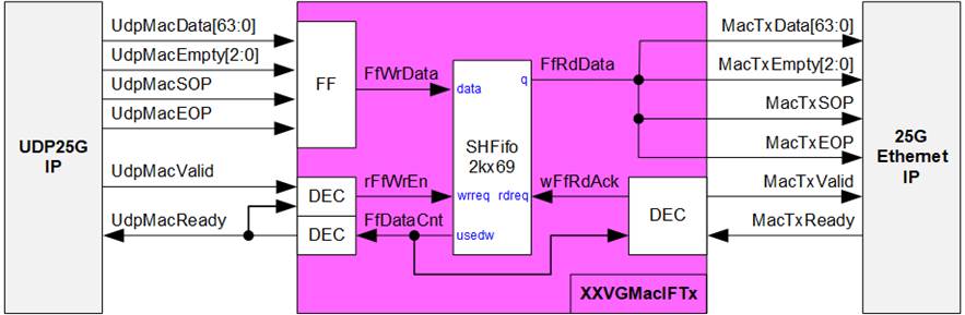
Figure 2‑2 XXVGMacIFTx Block Diagram
Tx interface timing diagram of 25G Ethernet hard IP and UDP25G-IP are different. UDP25G-IP needs to send data of one packet continuously, but Intel EMAC does not support this feature. Intel EMAC may de-assert ready signal to pause receiving data before end of the packet. XXVGMacIFTx is designed to store transmitted data from UDP25G-IP when 25G Ethernet IP is not ready to receive new data. The FIFO depth is 2048 to store at least one data packet during pausing time. Maximum packet size of UDP25G-IP is 8960 bytes or 1120 data. Therefore, 2048 is enough for storing one packet. The FIFO is show-ahead FIFO which the read data is valid for reading before asserting read enable to ‘1’. After read enable of FIFO is asserted to ‘1’, the next read data is valid on read data bus in the next clock cycle.
The operation of XXVGMacIFTx is split into two parts. First is the logic for transferring a packet from UDP25G-IP to FIFO. Second is the logic for transferring a packet from FIFO to 25G Ethernet IP. Timing diagrams of each part are displayed in Figure 2‑3 and Figure 2‑4.
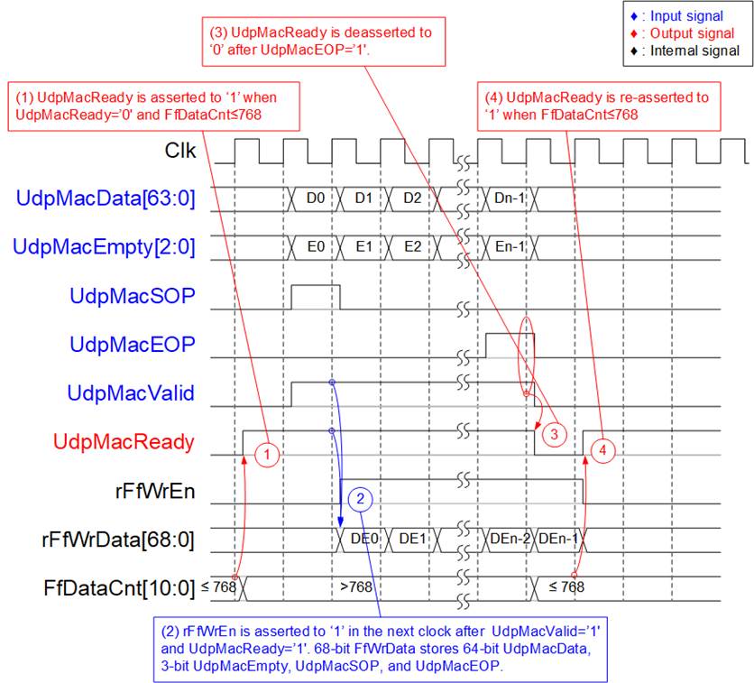
Figure 2‑3 Timing diagram of data transferring from UDP25G-IP to FIFO
(1) Before asserting UdpMacReady to ‘1’ for receiving the new packet from UDP25G-IP, two conditions must be met. First, free space in FIFO is enough for storing maximum packet size, 9014 bytes. For simple monitoring logic, the upper bit of FfDataCnt is read to confirm the amount of data in FIFO is not more than 768 (free space is more than 1279). Second, the previous packet is completely transferred, monitored by UdpMacReady=’0’.
(2) UDP25G-IP starts transmitting a packet by asserting UdpMacValid to ‘1’. The input signals from UDP25G-IP (UdpMacData, UdpMacEmpty, UdpMacSOP, and UdpMacEOP) are valid and stored to FIFO when UdpMacValid and UdpMacReady are asserted to ‘1’. After that, the inputs are stored to FIFO by asserting rFfWrEn to ‘1’. 69-bit write data to FIFO consists of 64-bit data (UdpMacData), 2-bit empty byte (UDPMacEmpty), start flag (UdpMacSOP), and end flag (UdpMacEOP).
(3) After receiving the last data of a packet (UdpMacEOP=’1’ and UdpMacValid=’1’), UdpMacReady is de-asserted to ‘0’ to pause data transmission for monitoring FfDataCnt.
(4) If FfDataCnt shows ready status, UdpMacReady will be re-asserted to ‘1’ in the next cycle.
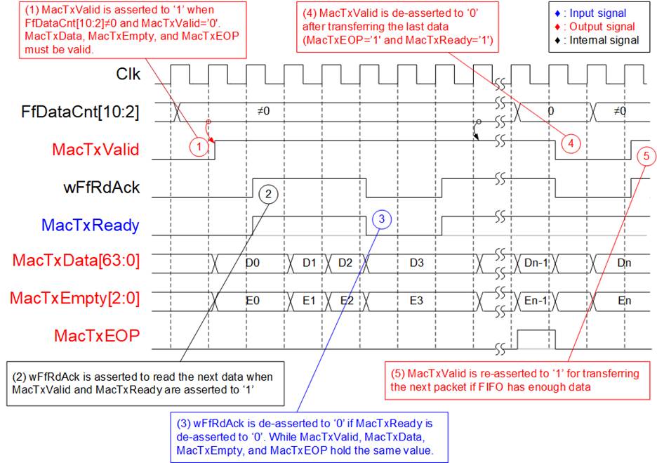
Figure 2‑4 Timing diagram of data transferring from FIFO to 25G Ethernet IP
(1) The new packet starts transmission when the FIFO stores some data (FfDataCnt[10:2] ≠ 0) and the packet is not transmitting (MacTxValid=’0’). To start data transmission, MacTxValid is asserted to ‘1’ with the valid output signals to Ethernet IP, i.e., 64-bit MacTxData, 3-bit MacTxEmpty, MacTxSOP, and MacTxEOP.
(2) If the data is transmitted to Ethernet IP completely (MacTxValid=’1’ and MacTxReady=’1’), wFfRdAck is asserted to ‘1’ to read the next data from FIFO.
(3) If MacTxReady is de-asserted to ‘0’, wFfRdAck will be de-asserted to ‘0’ to pause reading new data from FIFO. All output signals to Ethernet IP hold the same value until Ethernet IP re-asserts MacTxReady to 1’.
(4) After the last data of a packet is transferred completely (MacTxEOP=’1’ and MacTxReady=’1’), MacTxValid is de-asserted to ‘0’ to pause data transmission.
(5) The next packet is transmitted when FIFO has the data. It returns to step 1 to transmit the new packet.
2.3 XXVGMacIFRx (only when using 25G Ethernet IP for Agilex)
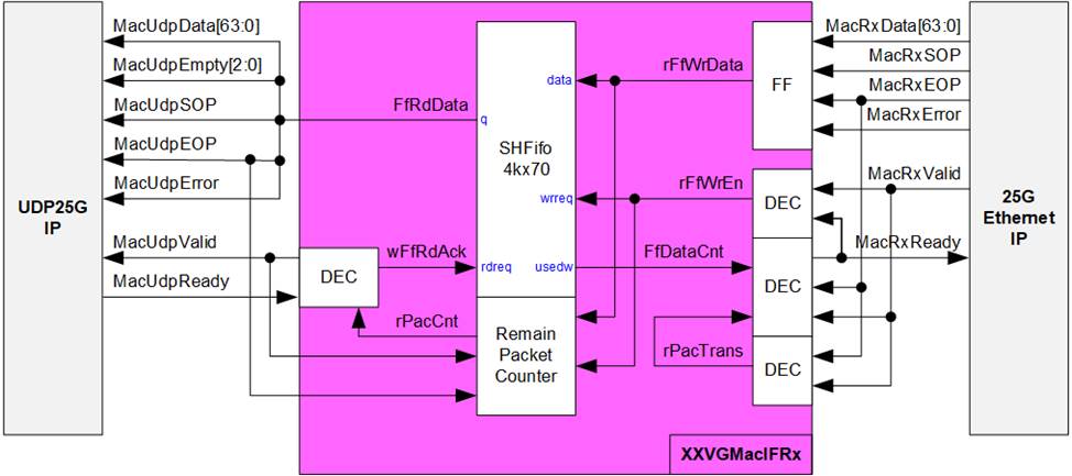
Figure 2‑5 XXVGMacIFRx Block Diagram
Rx interface timing diagram of 25G Ethernet hard IP and UDP25G-IP are different. UDP25G-IP needs to receive data of one packet continuously, but Intel EMAC does not support this feature. 25G Ethernet IP may de-assert valid signal to pause transmitting data before end of the packet. XXVGMacIFRx is designed to store transmitted data from 25G Ethernet IP when data transmission is paused. The FIFO depth is 4096 which is enough for storing several Ethernet packets. The FIFO is show-ahead FIFO, similar to XXVGMacIFTx.
Remain packet counter is designed to count the number of packets stored in the FIFO. The counter is increased when the new packet is received from 25G Ethernet IP while the counter is decreased when the packet is transferred to UDP25G-IP completely.
The operation of XXVGMacIFRx is split into two parts. First is the logic for transferring a packet from 25G Ethernet IP to FIFO. Second is the logic for transferring a packet from FIFO to UDP25G-IP. Timing diagrams of each part are displayed Figure 2‑6 and Figure 2‑7.
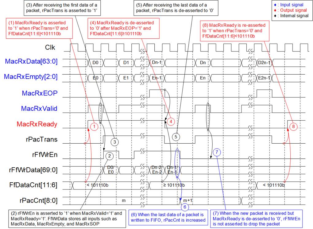
Figure 2‑6 Timing diagram of data transferring from 25G Ethernet IP to FIFO
(1) Bit[11:6] of FfDataCnt is monitored to check the free space size. If bit[11:6] of FfDataCnt is less than 101110b (FfDataCnt<2944), the free space in FIFO is more than 1153 which is enough for storing maximum packet size (9014 bytes). Also, rPacTrans is monitored to confirm the packet is not transmitting (rPacTrans=’0’). After that, MacRxReady is asserted to ‘1’ to start data reception from Ethernet IP.
(2) MacRxValid is asserted to ‘1’ to transfer the new packet, the data and control signals from Ethernet IP are stored to FIFO, i.e., 64-bit MacRxData, 3-bit MacRxEmpty, MacRxSOP, MacRxEOP, and MacRxError. Therefore, rFfWrEn is asserted to ‘1’ to write the FIFO and the write data is 70-bit FfWrData to store the data and control signals.
(3) After the first data of a packet is received, rPacTrans is asserted to ‘1’ until end of a packet. Therefore, rPacTrans is applied to monitor the packet transmission status.
(4) If the last data of a packet is received and free space size in FIFO is not enough (FFDataCnt≥2944), MacRxReady will be de-asserted to ‘0’ to pause data reception.
(5) After the last data of a packet is received, rPacTrans is de-asserted to ‘0’ to change packet transmission status from Busy to Idle.
(6) After storing the last data of a packet to FIFO (rFfWrEn=’1’ and rFfWrData[67] which is EOP flag =’1’), rPacCnt which is the counter to show total number of packet stored in FIFO is increased by 1.
(7) If the next packet is received but MacRxReady is de-asserted to ‘0’, the received packet will be dropped and not be stored to FIFO.
(8) MacRxReady is re-asserted to ‘1’ when there is no packet transmitted and free space size in FIFO is enough.

Figure 2‑7 Timing diagram of data transferring from FIFO to UDP25G-IP
(1) Before starting transferring a packet from FIFO to UDP25G-IP when at least one packet is stored in FIFO and UDP25G-IP is ready to receive packet. rPacCnt shows the number of packets stored in FIFO and it must not be equal to 0 to confirm at least one packet is available. After MacUdpReady is asserted to ‘1’ by UDP25G-IP, MacUdpValid is asserted to ‘1’ to start data transmission.
(2) After each data is transferred to UDP25G-IP completely (MacUdpValid=’1’ and MacUdpReady=’1’), wFfRdAck is asserted to ‘1’ to read the next data. The read data output from FIFO are applied to be the data and control signals sent to UDP25G-IP, i.e., 64-bit MacUdpData, 3-bit MacUdpEmpty, MacUdpSOP, MacUdpEOP, and MacUdpError. MacUdpValid and wFfRdAck are asserted to ‘1’ until the end of packet to transfer the data and control signals to UDP25G-IP continuously.
(3) After the last data of a packet is transferred (aMacUdpEOP=’1’ and MacUdpValid=’1’), MacUdpValid and wFfRdAck are de-asserted to ‘0’ to pause a packet transmission. Also, rPacCnt are decreased by 1 after completing transferring one packet.
2.4 UDP25G-IP
UDP25G-IP implements UDP/IP stack and offload engine. User interface has two signal groups - control signals and data signals. Control and status signals use Single-port RAM interface for write/read register access. Data signals use FIFO interface for transferring data stream in both directions. More details are described in datasheet.
More details are described in datasheet.
https://dgway.com/products/IP/UDP25G-IP/dg_udp25gip_data_sheet_intel.pdf
2.5 CPU and Peripherals
32-bit Avalon-MM is applied to be the bus interface for the CPU accessing the peripherals such as Timer and JTAG UART. To control and monitor the test system, the control and status signals are connected to register for CPU access as a peripheral through 32-bit Avalon-MM bus. CPU assigns the different base address and the address range to each peripheral for accessing one peripheral at a time.
In the reference design, the test hardware is connected as a peripheral of CPU system with specified base address and range. Therefore, Avl2Reg module that interfaces with CPU must support Avalon-MM bus standard for supporting CPU writing and reading, as shown in Figure 2‑8.
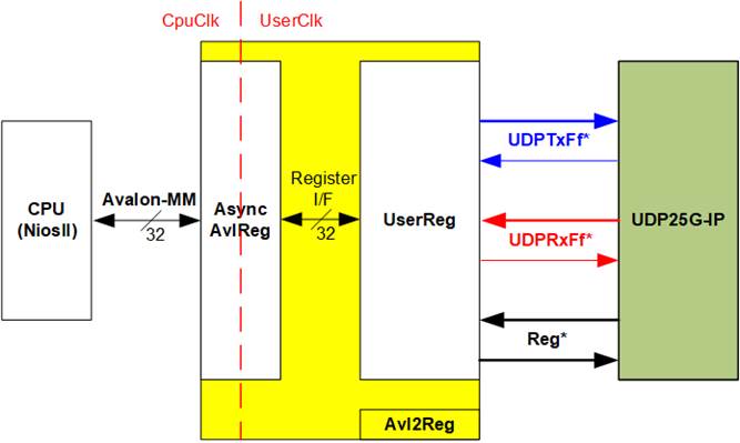
Figure 2‑8 Avl2Reg block diagram
Avl2Reg consists of AsyncAvlReg and UserReg. AsyncAvlReg is designed to convert the Avalon-MM signals to be the simple register interface which has 32-bit data bus size (similar to Avalon-MM data bus size). Besides, AsyncAvlReg includes asynchronous logic to support clock domain crossing between CpuClk and UserClk.
UserReg includes the register file of the parameters and the status signals of test logics. The data interface and control interface of UDP25G-IP are connected to UserReg. More details of AsyncAvlReg and UserReg are described as follows.
2.5.1 AsyncAvlReg
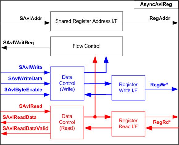
Figure 2‑9 AsyncAvlReg interface
The signal on Avalon-MM bus interface can be split into three groups, i.e., Write channel (blue color), Read channel (red color), and Shared control channel (black color). More details of Avalon-MM interface specification are described in following document.
https://www.intel.com/content/dam/www/programmable/us/en/pdfs/literature/manual/mnl_avalon_spec.pdf
According to Avalon-MM specification, one command (write or read) can be operated at a time. The logics inside AsyncAvlReg are split into three groups, i.e., Write control logic, Read control logic, and Flow control logic. Flow control logic controls SAvlWaitReq to hold the next request from Avalon-MM interface if the current request does not finish. Write control and Write data I/F of Avalon-MM bus are latched and transferred to be Write register interface with clock domain crossing registers. Similarly, Read control I/F are latched and transferred to be Read register interface with clock domain crossing registers. After that, the returned data from Register Read I/F is transferred to Avalon-MM bus by using clock domain crossing registers. Address I/F of Avalon-MM is latched and transferred to Address register interface as well.
The simple register interface is compatible with single-port RAM interface for write transaction. The read transaction of the register interface is slightly modified from RAM interface by adding RdReq and RdValid signals for controlling read latency time. The address of register interface is shared for write and read transaction, so user cannot write and read the register at the same time. The timing diagram of the register interface is shown in Figure 2‑10
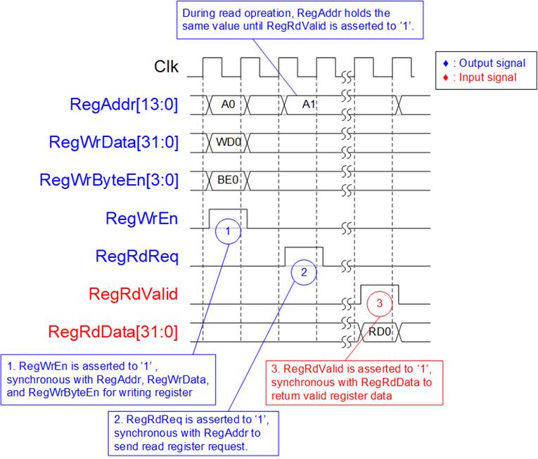
Figure 2‑10 Register interface timing diagram
1) To write register, the timing diagram is similar to single-port RAM interface. RegWrEn is asserted to ‘1’ with the valid signal of RegAddr (Register address in 32-bit unit), RegWrData (write data of the register), and RegWrByteEn (the write byte enable). Byte enable has four bits to be the byte data valid. Bit[0], [1], [2], and [3] are equal to ‘1’ when RegWrData[7:0], [15:8], [23:16], and [31:24] are valid respectively.
2) To read register, AsyncAvlReg asserts RegRdReq to ’1’ with the valid value of RegAddr. The slave detects RegRdReq asserted and starts the read transaction. During read operation, the address value (RegAddr) does not change the value until RegRdValid is asserted to ‘1’. Therefore, the address can be used for selecting the returned data by using multiple layers of multiplexer.
3) The read data is returned on RegRdData bus by the slave with asserting RegRdValid to ‘1’. After that, AsyncAvlReg forwards the read value to SAvlRead interface.
2.5.2 UserReg
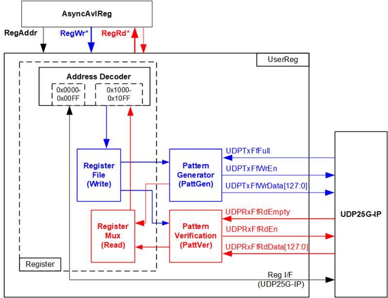
Figure 2‑11 UserReg block diagram
The logic inside UserReg has three operations, i.e., Register, Pattern generator (PattGen), and Pattern verification (PattVer). Register block decodes the address requested from AsyncAvlReg and then selects the active register for write or read transaction. Pattern generator block sends 128-bit test data to UDP25G-IP following FIFO interface standard. Pattern verification block reads and verifies 128-bit received data from UDP25G-IP following FIFO interface standard. More details of each block are described as follows.
Register Block
The address range, mapped to UserReg, is split into two areas, i.e., UDP25G-IP register (0x0000-0x00FF) and UserReg register (0x1000-0x10FF).
Address decoder decodes the upper bit of RegAddr for selecting the active hardware. The register file inside UserReg uses 32-bit data bus. Therefore, write byte enable (RegWrByteEn) is not applied in the test system and the CPU uses 32-bit pointer to set the hardware registers.
To read register, one multiplexer is designed to select the read data within each address area. The lower bit of RegAddr is applied in each Register area to select the active data. Next, the address decoder uses the upper bit to select the read data from the active area for returning to CPU. Totally, the latency of read data is equal to one clock cycle. Therefore, RegRdValid is created by RegRdReq with asserting one D Flip-flop. More details of the address mapping within UserReg module are shown in Table 2‑1
Table 2‑1 Register map Definition
|
Address |
Register Name |
Description |
|
Wr/Rd |
(Label in the “udp25gtest.c”) |
|
|
BA+0x0000 – BA+0x00FF: UDP25G-IP Register Area More details of each register are described in UDP25G-IP datasheet. |
||
|
BA+0x0000 |
UDP_RST_REG |
Mapped to RST register within UDP25G-IP |
|
BA+0x0004 |
UDP_CMD_REG |
Mapped to CMD register within UDP25G-IP |
|
BA+0x0008 |
UDP_SML_REG |
Mapped to SML register within UDP25G-IP |
|
BA+0x000C |
UDP_SMH_REG |
Mapped to SMH register within UDP25G-IP |
|
BA+0x0010 |
UDP_DIP_REG |
Mapped to DIP register within UDP25G-IP |
|
BA+0x0014 |
UDP_SIP_REG |
Mapped to SIP register within UDP25G-IP |
|
BA+0x0018 |
UDP_DPN_REG |
Mapped to DPN register within UDP25G-IP |
|
BA+0x001C |
UDP_SPN_REG |
Mapped to SPN register within UDP25G-IP |
|
BA+0x0020 |
UDP_TDL_REG |
Mapped to TDL register within UDP25G-IP |
|
BA+0x0024 |
UDP_TMO_REG |
Mapped to TMO register within UDP25G-IP |
|
BA+0x0028 |
UDP_PKL_REG |
Mapped to PKL register within UDP25G-IP |
|
BA+0x0034 |
UDP_TDH_REG |
Mapped to TDH register within UDP25G-IP |
|
BA+0x0038 |
UDP_SRV_REG |
Mapped to SRV register within UDP25G-IP |
|
BA+0x003C |
UDP_VER_REG |
Mapped to VER register within UDP25G-IP |
|
BA+0x0040 |
UDP_DML_REG |
Mapped to DML register within UDP25G-IP |
|
BA+0x0044 |
UDP_DMH_REG |
Mapped to DMH register within UDP25G-IP |
|
BA+0x1000 – BA+0x10FF: UserReg control/status |
||
|
BA+0x1000 |
Total transmit length (Low) |
Wr [31:0] – 32 lower bits of 44-bit total transmit size in 128-bit unit. Valid from 1-0xFFF_FFFF_FFFF. Rd [31:0] – 32 lower bits of 44-bit current transmit size in 128-bit unit. The value is cleared to 0 when USER_CMD_REG is written by user. |
|
Wr/Rd |
(USER_TXLENL_REG) |
|
|
BA+0x1004 |
Total transmit length (High) |
Wr [11:0] – 12 upper bits of 44-bit total transmit size in 128-bit unit. Rd [11:0] – 12 upper bits of 44-bit current transmit size in 128-bit unit. |
|
Wr/Rd |
(USER_TXLENH_REG) |
|
|
BA+0x1008 |
User command |
Wr [0] – Start transmitting. Set ‘0’ to start transmitting. [1] – Data verification enable (‘0’: Disable data verification, ‘1’: Enable data verification) Rd [0] – Tx Busy. (‘0’: Idle, ‘1’: Tx module is busy) [1] – Data verification error (‘0’: Normal, ‘1’: Error) This bit is auto-cleared when user starts new operation or reset. |
|
Wr/Rd |
(USER_CMD_REG) |
|
|
BA+0x100C |
User reset |
Wr [0] – Reset signal. Set ‘1’ to reset the logic. This bit is auto-cleared to ‘0’. [8] – Set ‘1’ to clear IntOut latched value Rd [8] – Latched value of IntOut, output from IP (‘0’: Normal, ‘1’: IntOut=’1’ is detected) This flag can be cleared by system reset condition or setting USER_RST_REG[8]=’1’. [16] – Ethernet linkup status from Ethernet MAC (‘0’: Not linkup, ‘1’: Linkup) |
|
Wr/Rd |
(USER_RST_REG) |
|
|
BA+0x1010 |
FIFO status |
Rd[3:0]: Mapped to UDPRxFfLastRdCnt signal of UDP25G-IP [15:4]: Mapped to UDPRxFfRdCnt signal of UDP25G-IP [24]: Mapped to UDPTxFfFull signal of UDP25G-IP |
|
Rd |
(USER_FFSTS_REG) |
|
|
BA+0x1014 |
Total receive length (Low) |
Rd[31:0] – 32 lower bits of 44-bit current receive size in 128-bit unit The value is cleared to 0 when USER_CMD_REG is written by user. |
|
Rd |
(USER_RXLENL_REG) |
|
|
BA+0x1018 |
Total receive length (High) |
Rd[11:0] – 12 upper bits of 44-bit current receive size in 128-bit unit |
|
Rd |
(USER_RXLENH_REG) |
|
|
BA+0x1080 |
EMAC IP version |
Rd[31:0] – Mapped to IPVersion output from DG EMAC-IP when the system integrates DG EMAC-IP. |
|
Rd |
(EMAC_VER_REG) |
|
Pattern Generator
Figure 2‑12 shows the details of PattGen which generates test data to UDP25G-IP while Figure 2‑13 shows the timing diagram of PattGen operation.
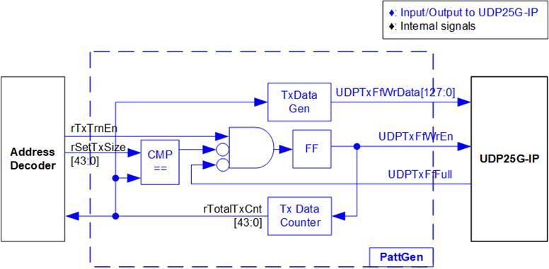
Figure 2‑12 PattGen block

Figure 2‑13 PattGen timing diagram
To start PattGen operation, the user sets USER_CMD_REG[0]=’0’ and then rTxTrnEn is asserted to ‘1’ until finishing the operation. When rTxTrnEn is ‘1’, UDPTxFfWrEn is controlled by UDPTxFfFull. UDPTxFfWrEn is de-asserted to ‘0’ to pause generating data when UDPTxFfFull is ‘1’. rTotalTxCnt is the data counter to check total number of transmitted data sent to UDP25G-IP. Also, the lower bits of rTotalTxCnt are used to generate 32-bit incremental data, output to UDPTxFfWrData signal. After all data is transferred completely, equal to rSetTxSize, rTxTrnEn is de-asserted to ‘0’.
Pattern Verification
Figure 2‑14 shows the details of PattVer which receives test data from UDP25G-IP. If data verification is enabled (rVerifyEn), the logic to verify data is run. Timing diagram of PattVer is displayed in Figure 2‑15.
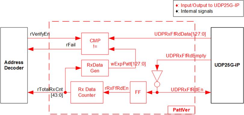
Figure 2‑14 PattVer block

Figure 2‑15 PattVer Timing diagram
3 CPU Firmware on FPGA
In reference design, CPU firmware is implemented as bare-metal OS for easily handling with the hardware. After the test system is run, the first step in the firmware is hardware initialization.

Figure 3‑1 Message on the console during initialization process
As shown in Figure 3‑1, there are four steps to initialize the hardware, described as follows.
1) After FPGA boot-up, 25G Ethernet link up status (USER_RST_REG[16]) is polling. The CPU waits until link up is detected. After that, displays welcome message to show IP information.
2) The menu to select the initialization mode of UDP25G-IP is displayed. The user can set as Client, Server, or Fixed-MAC mode.
Note:
- When running in Client mode, UDP25G-IP sends ARP request to get the MAC address of the target device from ARP reply. When running in Server mode, UDP25G-IP waits until ARP request is received to decode MAC address. Next, ARP reply is returned. When running Fixed-MAC mode, the user needs to know MAC address of the target device because UDP25G-IP does not transfer ARP packet.
- When running the test environment by using one FPGA board and Test PC, it is recommended to set FPGA to run as Client mode.
- When the test environment uses two FPGA boards, there are three solutions to initial the connection between two boards. First, one is Client and another is Server. Second, both are set to Fixed-MAC mode. Last, one is set to Fixed-MAC mode and another must be set to Client.
3) CPU displays default value of the network parameters, i.e., initialization mode, FPGA MAC address, FPGA IP address, FPGA port number, Target IP address, and Target port number. The firmware has two default parameter sets for the operation mode. First is the parameter set for Server mode and another is the parameter set for Client/Fixed-MAC mode. For Fixed-MAC mode, there is the extra parameter, Target MAC address. The user can select to complete the initialization process by using default parameters or updating some parameters. The details to change the parameter are described in Reset parameters menu (topic 3.2).
4) CPU waits until the IP completes the initialization process by checking if busy status (UDP_CMD_REG[0]) is equal to ’0’. After that, “IP initialization complete” is displayed with the main menu. There are five test operations in the main menu. More details of each operation are described as follows.
3.1 Display parameters
This menu is designed to display the current value of all UDP25G-IP parameters.
The step to display parameters is as follows.
1) Read the initialization mode.
2) Read all network parameters from each variable in firmware following the initialization mode, i.e., source (FPGA) MAC address, source (FPGA) IP address, source (FPGA) port number, target MAC address (only displayed in fixed MAC mode), target IP address, and target port number.
Note: The source parameters are FPGA parameters set to UDP25G-IP while the target parameters are the parameters of TestPC or another FPGA.
3) Print out each variable.
3.2 Reset parameters
This menu is used to change some UDP25G-IP parameters such as IP address and source port number. After setting the updated value to UDP25G-IP, the CPU resets the IP to start re-initialization process by using new parameters. Finally, the CPU waits until the initialization is completed.
The step to reset parameters is as follows.
1) Display all parameters on the console, similar to topic 3.1 (Display parameters).
2) Skip to the next step if the user uses the default value. Otherwise, the menu to set all parameters is displayed.
i. Receive initialization mode from the user. If the initialization mode is changed, the latest parameter set of new mode is displayed on the console.
3) Force reset to IP by setting UDP_RST_REG[0]=’1’.
4) Set all parameters to UDP25G-IP register such as UDP_SML_REG and UDP_DIP_REG.
5) De-assert IP reset by setting UDP_RST_REG[0]=’0’ to start IP initialization process.
6) Wait until busy flag (UDP_CMD_REG[0]) is asserted to ‘0’ after finishing the initialization process.
3.3 Send data test
This menu is designed to run sending data test. The user sets the parameters such as total transmit length. If the inputs are valid, the data is transferred by sending 32-bit incremental test data. The operation is finished when all data is completely transferred.
The step to send the data is as follows.
1) Receive two parameters from user, i.e., total transmit size and packet size. After that, CPU validates all inputs. The operation is cancelled if some inputs are invalid.
2) Set UserReg registers, i.e., transfer size (USER_TXLENL/H_REG), reset flag to clear initial value of test pattern (USER_RST_REG[0]=’1’), and command register to start data pattern generator (USER_CMD_REG=0). After that, test pattern generator in UserReg starts sending data to UDP25G-IP.
3) Display recommended parameters of test application on PC by reading current system parameters. Wait until user enters any keys to start IP sending data operation.
4) Set packet size to UDP25G-IP register (UDP_PKL_REG) and set total number of transmitted data to UDP_TDL/H_REG. After that, set Send command to UDP25G-IP (UDP_CMD_REG[0]=’1’) to run Send command.
5) Wait until the operation is completed by monitoring busy flag (UDP_CMD_REG[0]=’0’). During monitoring busy flag, CPU reads current number of transferred data from user logic (USER_TXLENL/H_REG) and displays the results on the console every second.
6) After the operation is completed, CPU calculates performance and displays test result on the console.
3.4 Receive data test
This menu is designed to run receiving data test. The user sets the parameters such as total receive length. If the inputs are valid, 32-bit incremental test data is created for verifying with the received data from PC/FPGA when the data verification is enabled.
The step to receive the data is as follows.
1) Receive two parameters, i.e., total transfer size and data verification mode from user input. The operation is cancelled if some inputs are invalid.
2) Set UserReg registers, i.e., reset flag to clear the initial value of test pattern (USER_RST_REG[0]=’1’) and data verification mode (USER_CMD_REG[1]=’0’/‘1’ to disable/enable).
3) Display recommended parameter (similar to Step 3 of Send data test).
4) Wait until total number of received data (USER_RXLENL/H_REG) is equal to the set value (complete condition) or the number of received data is not updated for 100 msec (timeout condition). During receiving data, CPU displays the current number of received data on the console every second.
5) Stop timer and check data verification status (USER_CMD_REG[1]). If the verification error is found, the error message will be displayed.
6) Calculate performance and then display test result on the console.
3.5 Full duplex test
This menu is designed to run full duplex test by transferring data between FPGA and another device (PC/FPGA) in both directions at the same time. The menu receives user parameters for running the test such as total transfer length. If all inputs are valid, the data starts transferring. The operation is finished when the data in both directions are completely transferred.
Note: When running the test with PC, the transfer size on the test application (udpdatatest) must be equal to the transfer size set on FPGA. Two “udpdatatest” are run by using different port number, one for sending data and another for receiving data. When running by FPGA and FPGA, the port number for sending and receiving data are similar.
The step to run full duplex test is as follows.
1) Receive three parameters, i.e., total transfer size (the same size for both transfer directions), packet size, and data verification mode (enable or disable) from user. The operation is cancelled if some inputs are invalid.
2) Set UserReg registers, i.e., transfer size (USER_TXLENL/H_REG), reset flag to clear the initial value of test pattern (USER_RST_REG[0]=’1’), and command register to start data pattern generator with data verification mode (USER_CMD_REG=0 or 2).
3) Display the recommended parameters of test application run on PC from the current system parameters.
4) Set packet size to UDP25G-IP register (UDP_PKL_REG) and set total number of transferred data to UDP_TDL/H_REG. After that, set Send command to UDP25G-IP (UDP_CMD_REG[0]=’1’) to run Send command. The IP starts sending data to the target device. At the same time, the IP is ready to receive data from the target.
5) CPU controls data flow of both directions at the same time. Therefore, there are two tasks running in the test, described as follows.
a. To send data, CPU reads busy flag (UDP_CMD_REG[0]) to wait until it is de-asserted to ‘0’. When Send command is finished, busy flag is de-asserted to ‘0’.
b. To receive data, CPU reads total number of received data. The read process is finished when total number of received data is equal to set value (no data lost). Otherwise, it is finished when total number of received data does not change for 100 msec (timeout).
When the data is not completely transferred, the current number of transmit data size (USER_TXLENL/H_REG) and receive data size (USER_RXLENL/H_REG) are read and displayed on the console every second.
6) Stop timer and check data verification status (USER_CMD_REG[1]). If the verification error is found, the error message will be displayed.
7) Calculate performance and display test result on the console.
3.6 Function list in User application
This topic describes the function list to run UDP25G-IP operation.
|
void init_param(void) |
|
|
Parameters |
None |
|
Return value |
None |
|
Description |
Reset parameters following the description in topic 3.2. In the function, show_param and input_param function are called to display parameters and get parameters from user. |
|
int input_param(void) |
|
|
Parameters |
None |
|
Return value |
0: Valid input, -1: Invalid input |
|
Description |
Receive network parameters from user, i.e., initialization mode, FPGA MAC address, FPGA IP address, FPGA port number, Target MAC address (when run in Fixed-MAC mode), Target IP address, and Target port number. If the input is valid, the parameter is updated. Otherwise, the value does not change. After receiving all parameters, calling show_param function to display parameters. |
|
void show_cursize(void) |
|
|
Parameters |
None |
|
Return value |
None |
|
Description |
Read current number of transmitted data and number of received data by reading USER_TXLENL/H_REG and USER_RXLENL/H_REG. Then, display the result in Byte, KByte, or MByte unit. |
|
void show_interrupt(void) |
|
|
Parameters |
None |
|
Return value |
None |
|
Description |
Read interrupt status from UDP_TMO_REG and decode interrupt type to display the details of interrupt on the console. |
|
void show_param(void) |
|
|
Parameters |
None |
|
Return value |
None |
|
Description |
Display the parameters following the description in topic 3.1. |
|
void show_result(void) |
|
|
Parameters |
None |
|
Return value |
None |
|
Description |
Read total transmit data size and total receive data size from USER_TXLENL/H_REG and USER_RXLENL/H_REG and display the results. Read total time usage from global parameters (timer_val and timer_upper_val) and calculate total time usage to display in usec, msec, or sec unit. Finally, transfer performance is calculated and displayed in MB/s unit. |
|
int udp_recv_test(void) |
|
|
Parameters |
None |
|
Return value |
0: The operation is successful -1: Receive invalid input or error is found |
|
Description |
Run Receive data test following description in topic 3.4. It calls show_interrupt, show_cursize, and show_result function. |
|
int udp_send_test(void) |
|
|
Parameters |
None |
|
Return value |
0: The operation is successful -1: Receive invalid input or error is found |
|
Description |
Run Send data test following description in topic 3.3. It calls show_cursize and show_result function. |
|
int udp_txrx_test(void) |
|
|
Parameters |
None |
|
Return value |
0: The operation is successful -1: Receive invalid input or error is found |
|
Description |
Run Full duplex test following described in topic 3.5. It calls show_interrupt, show_cursize, and show_result function. |
|
void wait_ethlink(void) |
|
|
Parameters |
None |
|
Return value |
None |
|
Description |
Read USER_RST_REG[16] and wait until ethernet connection is linked up |
4 Test Software on PC
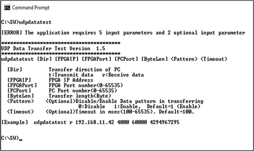
Figure 4‑1 “udpdatatest” application usage
“udpdatatest” is an application on PC for sending or receiving UDP payload data. There are five parameters and two optional parameters. To run the test, the parameters must be matched to parameter set on FPGA. More details of each parameter input are as follows.
1) Dir: : t – when PC sends data to FPGA
: r – when PC receives data from FPGA
2) FPGAIP : IP address setting on FPGA (default value in is 192.168.25.42)
3) FPGAPort : Port number of FPGA (default value in FPGA is 4000)
4) PCPort : PC port number for sending or receiving data
(default is 61000 for PC to FPGA and 60000 for FPGA to PC)
5) ByteLen : Transfer length for sending or receiving in byte unit. This value must be
aligned to 16 from UDP25G-IP limitation.
6) Pattern (optional): Default value when user does not input this parameter is 1.
0 – Generate dummy data in transmit mode or disable data verification
in receive mode.
1 – Generate incremental data in transmit mode or enable data verification in receive mode.
7) Timeout (optional): Timeout for receiving data in msec unit.
Default value when user does not input this parameter is 100.
100 ms is recommended value for running with UDP25G-IP.
Transmit data mode
The step when running the test application in transmit mode is described as follows.
1) Get parameters from user and verify that the input is valid.
2) Create the socket and then set properties of receive buffer.
3) Set IP address and port number from user parameters and then connect.
4) Send data to the send buffer for transmitting data. During sending data, the application prints total number of sent data on the console every second.
a) When Pattern=1, the send buffer is filled by 32-bit incremental pattern.
b) When Pattern=0, the send buffer is not filled. Dummy data is applied in the test.
5) After finishing sending all data, the application displays performance with total transmit data size as a test result.
Receive data mode
The step when running the test application in receive mode is described as follows.
1) Follow step (1)-(3) in Transmit data mode.
2) Repeat to read data until total number of received data is equal to set value. Otherwise, it is cancelled when there is no new received data until timeout. During reading data, the application prints total number of received data on the console every second.
a) When Pattern=1, the read data is verified by 32-bit incremental pattern which is increased every 4-byte received data.
b) When Pattern=0, the read data is not verified.
3) When the read loop is finished by timeout condition, “Timeout” message is displayed with total number of lost data and total number of received data.
4) After finishing the operation, the application displays performance as a test result.
5 Revision History
|
Revision |
Date |
Description |
|
1.0 |
8-Jul-21 |
Initial version release |