UDP40G-IP Core Data Sheet
Low Latency 40G Ethernet Intel FPGA IP

Core Facts |
|
|
Provided with Core |
|
|
Documentation |
User Guide, Design Guide |
|
Design File Formats |
Encrypted HDL |
|
Instantiation Templates |
VHDL |
|
Reference Designs & Application Notes |
QuartusII Project, See Reference Design Manual |
|
Additional Items |
Demo on Arria10 GX board |
|
Support |
|
|
Support Provided by Design Gateway Co., Ltd. |
|
Design Gateway Co.,Ltd
E-mail: ip-sales@design-gateway.com
URL: www.design-gateway.com
Features
· UDP/IP stack implementation
· Support IPv4 protocol
· Full-duplex transferring by using two port numbers for each transfer direction
· Support more sessions by using multiple UDP40G IPs
· Support Jumbo frame
· Packet size for transmit must be aligned to 256-bit because Transmit data bus size is 256-bit
· Received data bus size is 256-bit, so total receive size must be aligned to 256-bit
· Transmit/Receive buffer size, adjustable for optimizing resource and performance
· Simple data interface by standard FIFO interface
· Simple control interface by single port RAM interface
· 256-bit FIFO interface with Ethernet MAC
· At least 200 MHz is recommended for clock input to UDP40G IP
· Reference design available on Arria10 GX development kit
· Support IP fragmentation feature
· Customized service for following features
· Multicast IP
· Unaligned 256-bit data transferring
· Network parameter assignment by other methods
Table 1: Example Implementation Statistics
|
Family |
Example Device |
Fmax (MHz) |
ALMs1 |
Registers1 |
Pin |
Block Memory bit2 |
Design Tools |
|
Arria 10 GX |
10AX115S2F45I1SG |
275 |
2,678 |
4,336 |
- |
1,179,648 |
QuartusII18.0 |
Notes:
1) Actual logic resource dependent on percentage of unrelated logic
2) Block memory resources are based on 64kB Tx data buffer size and 64kB Rx data buffer size.
Applications
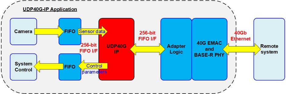
Figure 1: UDP40G IP Application
Figure 1 shows the example application of video camera system. The video data from camera is streaming to the FIFO and forwarded to remote system via 40 Gb Ethernet by UDP40G IP. UDP40G IP is desigend to support bi-directional transfer by using different port numbers at the same time, so Remote system can send the updated parameters for real-time controlling the system via 40 Gb Ethernet.
General Description
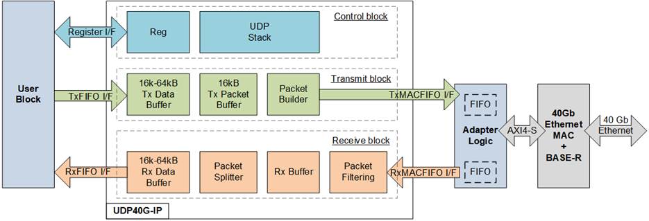
Figure 2: UDP40G IP Block Diagram
UDP40G IP core implements UDP/IP stack by hardware logic and connects EMAC and PCS/PMA (BASE-R) module through Adapter logic as the lower layer hardware. User interface of UDP40G IP consists of two interfaces, i.e. Register interface for control signals and FIFO interface for data signals.
Register interface has 4-bit address for accessing up to 16 registers, consisting of network parameters, command register and system parameters. The IP uses two sessions for transferring data in bi-directional, one session for one direction. All network parameters of both sessions must be similar, except the port number on the target device. The network parameters are assigned by the user to be fixed value for both UDP40G IP and the target device before starting IP initialization. The reset process is necessary when some network parameters must be changed. The initialization process has two modes to get MAC address of the target device. After finishing the initialization process, the IP is ready for transferring data with the target device.
To send the data, the user sets total transfer size and packet size to the IP and then transfers the data via TxFIFO interface which is 256-bit data size. When the data is received from the target, the user reads the received data from the IP via RxFIFO interface.
To meet the user system requirement which may be sensitive on the memory resource or the performance, the buffer size inside the IP can be assigned by the user. Tx data buffer and Rx data buffer can be adjusted for Tx path and Rx path respectively. Buffer size in the IP is applied to be the data buffer between user logic and EMAC. Using bigger buffer size, the user logic can switch to run other tasks for longer time before switching back to transfer the data with UDP40G IP.
Functional Description
UDP40G IP core can be divided into three parts, i.e. control block, transmit block and receive block.
Control Block
· Reg
Table 2: Register map Definition
|
RegAddr [3:0] |
Reg Name |
Dir |
Bit |
Description |
|
0000b |
RST |
Wr /Rd |
[0] |
Reset IP. ‘0’: No reset, ‘1’: Reset. Default value is ‘1’. After all parameters are assigned, the user sets ‘0’ to this register for loading parameters and start system initialization. User must set this register to ‘1’ and ‘0’ respectively when some network paramters are changed. The network parameters controlled by RST register are SML, SMH, DIP, SIP, DPN, SPN and SRV register. |
|
0001b |
CMD |
Wr |
[0] |
User command. Set ‘1’ to start sending data. Before setting this register to start new operation, user needs to confirm that the system is in Idle status by checking busy signal de-asserted to ‘0’. Busy signal is the IP output and can be read by bit[0] of CMD register. |
|
Rd |
[0] |
System busy flag. ‘0’: Idle, ‘1’: IP is busy from initialization or send command. This signal is also mapped as Busy (IP output signal). |
||
|
0010b |
SML |
Wr /Rd |
[31:0] |
Define 32-bit lower MAC address (bit [31:0]) for this IP. To update this value, the IP must be reset by RST register. |
|
0011b |
SMH |
Wr /Rd |
[15:0] |
Define 16-bit upper MAC address (bit [47:32]) for this IP. To update this value, the IP must be reset by RST register. |
|
0100b |
DIP |
Wr /Rd |
[31:0] |
Define 32-bit target IP address. To update this value, the IP must be reset by RST register. |
|
0101b |
SIP |
Wr /Rd |
[31:0] |
Define 32-bit IP address for this IP. To update this value, the IP must be reset by RST register. |
|
0110b |
DPN |
Wr /Rd |
[31:0] |
[15:0]-Define 16-bit target port number for IP sending data. [31:16]-Define 16-bit target port number for IP receiving data. To update this value, the IP must be reset by RST register. |
|
0111b |
SPN |
Wr /Rd |
[15:0] |
Define 16-bit port number for this IP. To update this value, the IP must be reset by RST register. |
|
1000b |
TDL |
Wr |
[31:0] |
32-lower bit of 48-bit total Tx data length in byte unit which must be aligned to 32-byte. Valid range is 32 – 0xFFFFFFE0 (Bit[4:0] is ignored by the IP). User needs to set this register before setting CMD register=’1’. The IP loads TDL/TDH register when CMD register is set. After the IP runs Send data command (Busy=’1’), the user can set the new value of TDL/TDH register for the next command. The user does not need to set TDL/TDH register again when the next command uses the same total data length. |
|
Rd |
32-lower bit of 48-bit remaining data length in byte unit which does not transmit. |
|
RegAddr [3:0] |
Reg Name |
Dir |
Bit |
Description |
|
1001b |
TDH |
Wr |
[15:0] |
16-upper bit of 48-bit total Tx data length in byte unit. More details are described in TDL register description. |
|
Rd |
16-upper bit of 48-bit remaining data length in byte unit. More details are described in TDL register description. |
|||
|
1010b |
TMO |
Wr |
[31:0] |
Define timeout value for waiting ARP reply packet after sending ARP request. The counter is run under Clk input, so timer unit is equal to 1/Clk (5 ns when Clk is 200 MHz). IntOut is asserted to ‘1’ when the ARP reply is not received in time. This value should be more than latency time in the network to generate timeout. |
|
Rd |
The details of timeout interrupt. [0]-Timeout from not receiving ARP reply packet After timeout, IP resends ARP request until ARP reply is received. [8]-Rx packet ignored because of Rx data buffer full [9]-Rx packet ignored because of checksum failed [10]-Rx packet ignored because of received packet error from EMAC ( MacRxFfRdData[257]=’1’). |
|||
|
1011b |
PKL |
Wr /Rd |
[15:0] |
UDP data length of one Tx packet in byte unit, but the length must be aligned to 32-byte. Valid from 32-16000. Default value is 1472 byte which is the maximum size for non-jumbo frame that is aligned to 32-byte. Bit[4:0] of this register is ignored by the IP. During running Send data command (Busy=’1’), the user must not set this register. Similar to TDL/TDH register, the user does not need to set PKL register again when the next command uses the same packet length. |
|
1110b |
SRV |
Wr/ Rd |
[0] |
‘0’: Client mode (default). After RST register changes from ‘1’ to ‘0’, the IP sends ARP request to get Target MAC address from the ARP reply returned by the target device. IP busy is deasserted to ‘0’ after receiving ARP reply. ‘1’: Server mode. After RST register changes from ‘1’ to ‘0’, the IP waits ARP request from the Target to get Target MAC address. After receiving ARP request, the IP generates ARP reply and then de-asserts IP busy to ‘0’. Note: In Server mode, when RST register changes from ‘1’ to ‘0’, the target device needs to resend ARP request for UDP40G IP completing the IP initialization. |
|
1111b |
VER |
Rd |
[31:0] |
IP version |
· UDP Stack
After RST register changes from ‘1’ to ‘0’, the initialization phase begins. There are two modes for running the initialization phase, set by SRV[0] register, i.e. Client mode or Server mode. The parameters from Reg module is read by UDP Stack and then set to Transmit block and Receive block for transferring the packet to complete the initialization process, following the mode. After that, the IP changes to data transferring phase.
UDP40G IP supports full-duplex transfer, so UDP40G IP can send data to the target device and receive data from the target device at the same time. Busy signal is asserted to ‘1’ during sending data and de-asserted to ‘0’ after finishing sending data.
To send the data, the data from the user is stored in Tx data buffer and Tx packet buffer. After the network parameters are read to build UDP header by Packet Builder, Transmit block sends UDP packet including the data from the user to the target device via Ethernet MAC.
When the data is received by Receive block, Busy signal is not asserted. UDP Stack does not need to send any packet to confirm the received data, so UDP Stack is available for running Send command. Full-duplex transfer can be run with full performance.
Table 3: TxBuf/RxBufBitWidth Parameter description
|
Value of BitWidth |
Buffer Size |
TxBufBitWidth |
RxBufBitWidth |
|
9 |
16kByte |
Valid |
Valid |
|
10 |
32kByte |
Valid |
Valid |
|
11 |
64kByte |
Valid |
Valid |
Transmit Block
· Tx Data Buffer
This buffer size is set by “TxBufBitWidth” parameter of the IP. The valid value is 9-11 which is equal to the address size of 256-bit buffer, as shown in Table 3. The buffer size should be more than or equal to two times of Tx Packet Size, set by PKL register. If Tx data buffer always stores at least two packet data, UDP40G IP can transfer data to EMAC continuously and the system can get the best transmit performance on 40Gb Ethernet. Also, this buffer is the data buffer for the user logic. Using the bigger size allows the user logic to have longer time for switching to run other tasks before going back to handle with the data interface of Tx data buffer.
· Tx Packet Buffer
This buffer size is 16 Kbyte to store at least one transmit packet. Data in Tx packet buffer is forwarded to EMAC.
· Packet Builder
UDP packet consists of the header and the data. Packet builder receives network parameters, set in Reg module, and then prepares UDP header. Also, IP and UDP checksum are calculated to be UDP header. After that, all UDP header is built, the header combining with the data from Tx packet buffer is transmitted to EMAC.
Receive Block
In the receive block, Rx data buffer is included to store the received data from the target device. The data is stored in the buffer when the header in the packet is matched and Rx data buffer size has free space enough. The header in the packet is compared with the network paramters, set by Reg module, and IP/UDP checksum must be correct. Otherwise, the received packet will be ignored.
· Rx Buffer
This is temporary buffer to store the received packets from EMAC when the previous packet is not completely processed.
· Packet Filtering
The header in Rx packet are verifed by this module to validate the packet. The packet is valid when the following conditions are met.
(1) Network parameters are matched to the value in register, i.e. MAC address, IP address and Port number.
(2) The packet is ARP packet or UDP/IPv4 packet.
(3) IP header length is valid (IP header length is equal to 20 bytes).
(4) IP data length and UDP data length must be matched.
(5) IP checksum and UDP checksum are correct or disabled.
Note: UDP checksum is not verifed for fragment packet.
(6) In case of fragment packet, the packet must be received in a good sequence, not swapped.
· Packet Splitter
This module is designed to remove the packet header and split only UDP data to store to Rx data buffer.
· Rx Data Buffer
This buffer size is set by “RxBufBitWidth” parameter of the IP. The valid value is 9-11 for 16Kbyte – 64Kbyte buffer size. This is the data buffer between user logic and UDP40G IP for receiving data operation. If user logic does not read data from Rx data buffer for long time until the buffer is full, the new received packet will be ignored. The minimum size of Rx data buffer is recommended to be equal to two times of receive packet size or more. Bigger buffer size can store more data when the user logic is not available to read data from UDP40G IP. The proper size depends on the unavailable time of the user logic.
User Block
This module can be designed by using state machine to set the command and the parameters via register interface. Also, the status can be monitored to confirm the operation is finished without any error. The data path can connect with the FIFO for sending or receiving data with the IP.
Low Latency 40G Ethernet Intel FPGA IP
The reference design uses 40G Ethernet MAC and PHY IP from Intel FPGA which can check for more details from following website.
https://www.intel.com/content/dam/www/programmable/us/en/pdfs/literature/ug/ug_ll_40gbe.pdf
Core I/O Signals
Descriptions of all parameters and I/O signals are provided in Table 4 and Table 5. The EMAC interface of the IP uses 256-bit FIFO standard as Show-ahead mode.
Table 4: Core Parameters
|
Name |
Value |
Description |
|
TxBufBitWidth |
9-11 |
Setting Tx Data buffer size. The value is the address bus size of this buffer. |
|
RxBufBitWidth |
9-11 |
Setting Rx Data buffer size. The value is the address bus size of this buffer. |
Table 5: Core I/O Signals
|
Signal |
Dir |
Description |
|
Common Interface Signal |
||
|
RstB |
In |
Reset IP core. Active Low. |
|
Clk |
In |
Clock input. Clock frequency should be at least 200 MHz to achieve the best performance. |
|
User Interface |
||
|
RegAddr[3:0] |
In |
Register address bus. In Write access, RegAddr is valid when RegWrEn=’1’. |
|
RegWrData[31:0] |
In |
Register write data bus. Valid when RegWrEn=’1’. |
|
RegWrEn |
In |
Register write enable. Valid at the same clock as RegAddr and RegWrData. |
|
RegRdData[31:0] |
Out |
Register read data bus. Valid in the next clock after RegAddr is valid. |
|
Busy |
Out |
IP busy status (‘0’-Idle, ‘1’-IP is busy from the intialization process or sending data) |
|
IntOut |
Out |
Timer interrupt. Assert to high for 1 Clock cycle when timeout is detected or Rx packet is ignored. More details of Interrupt status could be checked from TMO[10:0] register. |
|
Tx Data Buffer Interface |
||
|
UDPTxFfFull |
Out |
Asserted to ‘1’ when Tx data buffer is full. User needs to stop writing data within 4 clock cycles after this flag is asserted to ‘1’. |
|
UDPTxFfWrEn |
In |
Write enable to Tx data buffer. Asserted to ‘1’ to write data to Tx data buffer. |
|
UDPTxFfWrData[255:0] |
In |
Write data to Tx data buffer. Valid when UDPTxFfWrEn=’1’. |
|
Rx Data Buffer Interface |
||
|
UDPRxFfRdCnt[10:0] |
Out |
Data counter of Rx data buffer to show the number of received data in 256-bit unit. |
|
UDPRxFfLastRdCnt[4:0] |
Out |
Remaining byte of the last data in Rx data buffer when total received data in the buffer is not aligned to 32-byte unit. User cannot read the data until all 8-byte data is received. |
|
UDPRxFfRdEmpty |
Out |
Asserted to ‘1’ when Rx data buffer is empty. User needs to stop reading data immediately when this signal is asserted to ‘1’. |
|
UDPRxFfRdEn |
In |
Assert to ‘1’ to read data from Rx data buffer. |
|
UDPRxFfRdData[255:0] |
Out |
Data output from Rx data buffer. Valid in the next clock cycle after UDPRxFfRdEn is asserted to ‘1’. |
|
Signal |
Dir |
Description |
|
MAC FIFO Interface (Show-ahead mode) |
||
|
MacTxFfWrCnt[15:0] |
In |
Write data counter of MacTxFIFO in 256-bit. This signal is used to check full condition. If FIFO counter is less than 16-bit, please fill ‘1’ to upper bit. |
|
MacTxFfWrData[255:0] |
Out |
256-bit write data to MacTxFIFO. Valid at the same clock as MacTxFfWrEn=’1’. |
|
MacTxFfWrEn |
Out |
Assert to ‘1’ to write data to MacTxFIFO. This signal is always asserted to ‘1’ during transmitting one Tx packet. |
|
MacTxLastEmpty[4:0] |
Out |
Specify the number of bytes which are unused in the final word of the frame. This signal is valid when MacTxEnd=’1’ and MacTxFfWrEn=’1’. In IP core, this signal could be equal to two values, i.e. 0x16 (22 empty bytes) and 0x04 (4 empty bytes). |
|
MacTxSizeData[15:0] |
Out |
Total size of Tx packet in 256-bit unit. This value is stable during MacTxFfWrEn=’1’. Bit[15:11] is always equal to 0. |
|
MacTxEnd |
Out |
Assert to ‘1’ to indicate the final data of each Tx packet. |
|
MacRxFfEmpty |
In |
Empty flag of MacRxFIFO. Assert to ‘1’ when there is no data within MacRxFIFO. |
|
MacRxFfRdEn |
Out |
Assert to ‘1’ to read data from MacRxFIFO. This signal could be asserted to ‘1’ when MacRxFfEmpty=’0’. |
|
MacRxFfRdData[257:0] |
In |
Read data output from MacRxFIFO. This signal is valid at the same clock as MacRxFfRdEn=’1’. So, MacRxFIFO must be designed to run as Show-ahead mode. The definition of each received data is as follows. [255:0]: 256-bit received data from EMAC. [256]: Assert to ‘1’ to indicate the final data in each Rx packet from EMAC. [257]: ‘0’-normal packet, ‘1’-error packet. This bit must be asserted to ‘1’ at the same time as bit[256]=’1’ which indicates final data. |
Timing Diagram
IP Initialization
The initialization process begins after user changes RST register from ‘1’ to ‘0’. UDP40G IP can run in two modes, set by SRV[0] register, i.e. Client mode (SRV[0]=’0’) and Server mode (SRV[0]=’1’). The details of each mode are shown in the following timing diagram.

Figure 3: IP Initialization in Client mode
As shown in Figure 3, in Client mode UDP40G IP sends ARP request and waits ARP reply returned from the target device. Target MAC address is extracted from ARP reply packet. After finishing, Busy signal is de-asserted to ‘0’.
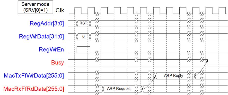
Figure 4: IP Initialization in Server mode
As shown in Figure 4, after reset process in Server mode, UDP40G IP waits ARP request sent by the target device. After that, UDP40G IP returns ARP reply to the target. Target MAC address is extracted from ARP request packet. Finally, Busy signal is de-asserted to ‘0’.
Register Interface
All control signals and the network parameters for the operation are set and monitored via Register interface. Timing diagaram of Register interface is similar to Single-port RAM which shares the address bus for write and read access. Read latency time of the read data from the address is one clock cycle. Register map is defined in Table 2.
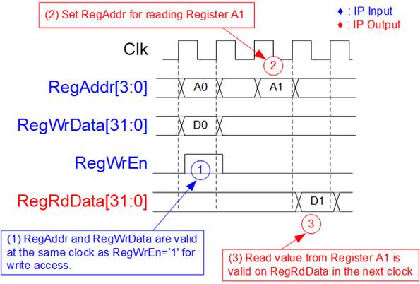
Figure 5: Register interface timing diagram
As shown in Figure 6, before the user sets CMD register to start the new command operation, Busy flag must be equal to ‘0’ to confirm that IP is in Idle status. After CMD register is set, Busy flag is asserted to ‘1’. Busy is de-asserted to ‘0’ when the command is completed.
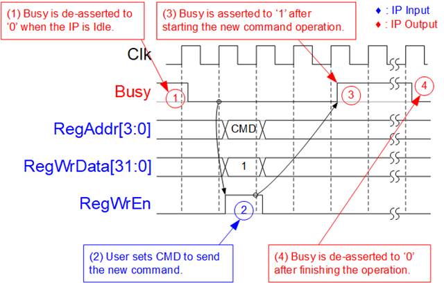
Figure 6: CMD register timing diagram
Tx FIFO Interface
To send the data to IP core via Tx FIFO interface, Full flag is monitored to be flow control signal. The write signals are similar to write interface of general FIFO by using write data and write enable as shown in as shown in Figure 7.
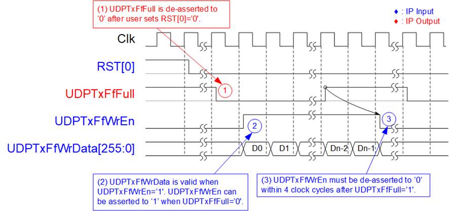
Figure 7: Tx FIFO interface timing diagram
(1) During IP is in reset condition, UDPTxFfFull is asserted to ‘1’ and all data in FIFO are flushed.
(2) Before sending data, user needs to confirm that full flag (UDPTxFfFull) is not asserted to ‘1’. After that, UDPTxFfWrEn can be asserted to ’1’ with valid value of UDPTxFfWrData.
(3) UDPTxFfWrEn must be de-asserted to ‘0’ within 4 clock cycles to pause data sending after UDPTxFfFull is asserted to ‘1’.
Rx FIFO Interface
After the received data is stored in Rx data buffer, the user can read the data from Rx data buffer by using Rx FIFO interface. Empty flag is monitored to check data available status and then asserts read enable signal to read the data, similar to read interface of general FIFO, as shown in Figure 8.

Figure 8: Rx FIFO interface timing diagram by Empty flag
(1) After the IP finishes reset process, there is no data in Rx data buffer (UDPRxFfEmpty=’1’).
(2) UDPRxFfEmpty is monitored to check data available status. When data is ready (UDPRxFfEmpty =’0’), UDPRxFfRdEn can be asserted to ‘1’ to read data from Rx data buffer.
(3) UDPRxFfRdData is valid in the next clock cycle.
(4) Reading data must be immediately paused by de-asserting UDPRxFfRdEn=’0’ when UDPRxFfEmpty =‘1’.
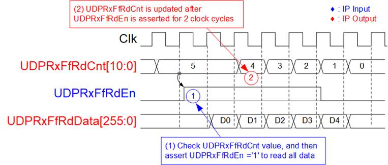
Figure 9: Rx FIFO interface timing diagram by using read counter
If user logic reads data as burst mode, UDP40G IP has read counter signal to show the total data stored in Rx FIFO interface as 256-bit unit. For example in Figure 9, there are five data available in Rx data buffer. So, user can assert UDPRxFfRdEn to ‘1’ for 5 clock cycles to read all data from Rx data buffer. The latency time between read counter (UDPRxFfRdCnt) and read enable (UDPRxFfRdEn) is 2 clock cycles.
MAC FIFO Interface
EMAC interface of UDP40G-IP is designed to be FIFO in Show-ahead mode interface. To integrate UDP40G IP with 40G EMAC, adapter logic including Show-ahead FIFO is recommended as shown in Figure 10.

Figure 10: UDP40G IP and EMAC connection
Before transmitting packet, UDP40G IP monitors MacTxFfWrCnt to check if free space inside MacTxFIFO is enough to store one packet. After that, MacTxFfWrEn is asserted to ‘1’ continuously until end of packet. MacTxFfWrData is valid at the same clock as MacTxFfWrEn=’1’. At the end of packet, MacTxEnd is asserted to ‘1’ with the valid MacTxLastEmpty. MacTxSizeData is stable during transmitting each packet to show total data of the packet in 256-bit unit. The example of timing diagram when UDP40G IP sends packet and packet size = n is shown in Figure 11.

Figure 11: MacTxFIFO interface timing diagram
(1) UDP40G IP starts transmitting the packet by asserting MacTxFfWrEn to ‘1’ with the valid data on MacTxFfWrData when free space of MacTxFf is enough for storing the packet (MacTxFfWrCnt <65535-n). The packet is transmitted continuously until the end of packet.
(2) During transmitting a packet, transmit packet size is valid on MacTxSizeData.
(3) MacTxEnd is asserted to ‘1’ with the valid byte enable of the last data on MacTxLastEmpty signal when transmitting the last data of the packet.
Figure 12 shows the example of MacRxFIFO interface when Rx packet size is equal to n. MacRxFfEmpty is applied to monitor data status in MacRxFIFO. The interface uses Show-ahead FIFO characteristic, so MacRxFfRdData is valid at the same clock as MacRxFfRdEn=’1’.
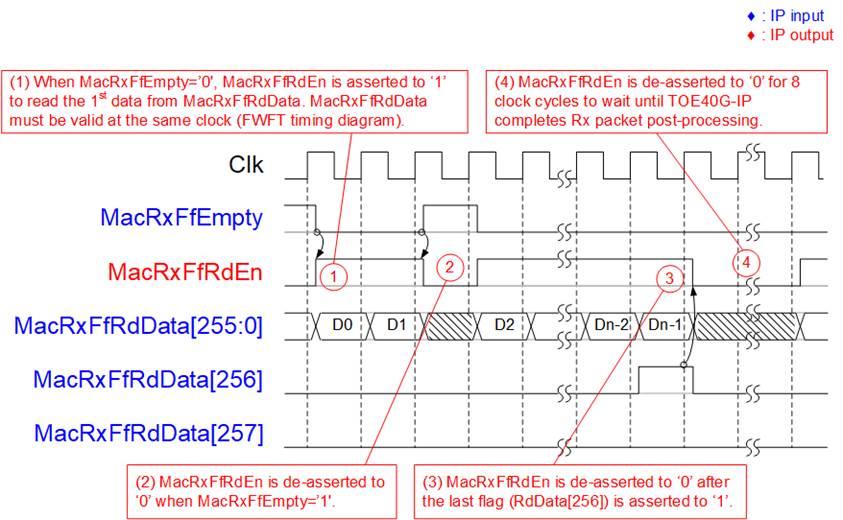
Figure 12: MacRxFIFO interface timing diagram
(1) UDP40G IP starts reading the received packet when MacRxFfEmpty is de-asserted to ‘0’. MacRxFfRdEn is asserted to ‘1’ to read the data and MacRxFfRdData is valid in the same clock cycle which is Show-ahead FIFO characteristic. 256-bit received data is placed on bit[255:0].
(2) During reading the packet, if data is not ready to read (MacRxFfEmpty=’1’), MacRxFfRdEn is de-asserted to ‘0’ to pause data reading in the same clock.
(3) Bit256 of MacRxFfRdData is asserted to ‘1’ when the last data of the packet is transferred. Also, bit257 of MacRxFfRdData is valid to check error status in this clock. MacRxFfRdEn is de-asserted to ‘0’ after receiving the last data for 8 clock cycles which is the time for IP post-processing the packet.
Example usage
Client mode (SRV[0]=’0’)
The example step to set register for transferring data in Client mode is shown as follows.
1) Set RST register=’1’ to reset the IP.
2) Set SML/SMH for MAC address, DIP/SIP for IP address and DPN/SPN for port number.
3) Set RST register=’0’ to start the IP initialization process by sending ARP request packet to get Target MAC address from ARP reply packet. Busy signal is de-asserted to ‘0’ after finishing the initialization process.
4) a. For data transmission, set TDL/TDH register (total transmit length) and PKL register (packet size). Next, set CMD register = ‘1’ to start data transmission. The user sends the data to UDP40G IP via TxFIFO interface before or after setting CMD register. When the command is finished, busy is de-asserted to ’0’. The user can set the new value to TDL/TDH, PKL and CMD register = ‘1’ to start the next transmission.
b. For data reception, user monitors RxFIFO status and reads data until RxFIFO is empty.
Server mode (SRV[0]=’1’)
Comparing to Client mode which MAC address is decoded from ARP reply packet after UDP40G IP sends ARP request packet, Server mode decodes MAC address from ARP request packet. The process for transferring data is the same as Client mode. The example step of Server mode is shown as follows.
1) Set RST register=’1’ to reset the IP.
2) Set SML/SMH for MAC address, DIP/SIP for IP address and DPN/SPN for port number.
3) Set RST register=’0’ to start the IP initialization process by waiting ARP request packet to get Target MAC address. Next, the IP creates ARP reply packet returned to the target device. After finishing the intialization, busy signal is de-asserted to ‘0’.
4) Remaining steps are similar to step 4 of Client mode.
Verification Methods
The UDP40G IP Core functionality was verified by simulation and also proved on real board design by using Arria10 GX development board.
Recommended Design Experience
User must be familiar with HDL design methodology to integrate this IP into the system.
Ordering Information
This product is available directly from Design Gateway Co., Ltd. Please contact Design Gateway Co., Ltd. For pricing and additional information about this product using the contact information on the front page of this datasheet.
Revision History
|
Revision |
Date |
Description |
|
1.0 |
21-Oct-2019 |
New release |
|
1.1 |
2-Oct-2020 |
Update company info |