UDP40G-IP Demo Instruction
Rev1.0 16-Jun-23
Part A UDP40G-IP demo by using FPGA and PC..
Part B UDP40G-IP demo by using two FPGAs
8.3 Send and Receive data Test (Half-duplex test)
1 Overview
The demo is designed to run UDP40G-IP for transferring 40 Gb Ethernet data by using UDP/IP protocol. Two test environments can be setup for the demo, as shown in Figure 1‑1. First test environment (Test Env#A) uses one FPGA board transferring data with TestPC. More details to run the demo by using FPGA and TestPC are described in PartA. Second test environment (Test Env#B) uses two FPGA boards to transfer data between the 1st FPGA and the 2nd FPGA. More details to run the demo by using two FPGAs are described in PartB.
User interface for setting test parameters on FPGA and monitoring hardware status is JTAG UART.
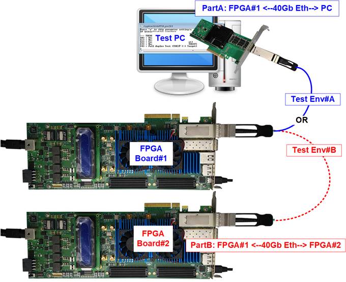
Figure 1‑1 Two test environments for the demo
Part A UDP40G-IP demo by using FPGA and PC
“udpdatatest” is test application to run on TestPC for transferring data with FPGA by using UDP/IP protocol. The input parameters of “udpdatatest” by user are transfer direction (transmit or receive data), transfer size, network parameters, and test mode. Half-duplex test with UDP40G-IP is operated by running one “udpdatatest” application on Windows command prompt (PC) while Full-duplex test with UDP40G-IP is operated by running two “udpdatatest” applications on two Windows command prompts (PC). Two applications for full-duplex test must run in different transfer direction (one for sending data and another for receiving data) by using different port number. More details of the demo are described as follows.
2 Environment Setup
To run UDP40G-IP demo by using FPGA and PC, please prepare following test environment.
1) FPGA development boards (Arria10 GX development kit)
2) PC with 40 Gigabit Ethernet support or 40 Gigabit Ethernet card
3) QSFP+ AOC cable for 40G network connection between FPGA board and 40G Ethernet card plugged-in on PC
4) micro USB cable for programming FPGA and JTAG UART, connecting between FPGA board and PC
5) “udpdatatest.exe” which is test application provided by Design Gateway, installed on PC
6) QuartusII programmer for programming FPGA and NiosII command shell, installed on PC
Note: Test result in this document is captured by using following test environment.
[1] 40G Network Adapter: Intel XL710-Q1
[2] QSFP+ AOC: AOC-Q1Q1-001
http://www.10gtek.com/uploadfile/download/pdf/aoc_datasheet/10Gtek%20AOC-Q1Q1-xxx%20(JH)%20V1.0.pdf
[3] PC: Motherboard ASUS Z170-K, Intel i7-6700K CPU, 32 GB RAM
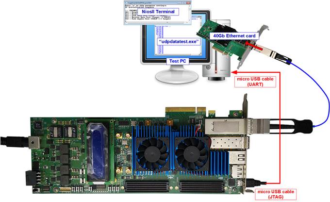
Figure 2‑1 UDP40G-IP demo (FPGA <-> PC) on Arria10 GX
3 PC Setup
Before running the demo, please check the network setting on PC. The example for setting the network is shown as follows.
3.1 IP Setting

Figure 3‑1 Setting IP address for PC
1) Open Local Area Connection Properties of 40-Gb connection, as shown in the left window of Figure 3‑1.
2) Select “TCP/IPv4” and then click Properties.
3) Set IP address = 192.168.40.25 and Subnet mask = 255.255.255.0, as shown in the right window of Figure 3‑1.
3.2 Speed and Frame Setting

Figure 3‑2 Set frame size = jumbo frame
1) On Local Area Connection Properties window, click “Configure” as shown in Figure 3‑2.
2) On Advanced Tab, select “Jumbo Packet”. Set Value to “9014 Bytes” for Jumbo Frame support or set value to “Disabled” for non-Jumbo Frame support, as shown in the lower window of Figure 3‑2.

Figure 3‑3 Performance option
3) On Advanced Tab, select “Performance Options” and click “Properties” button.
4) Set “Flow Control” = Disabled.
5) Set “Interrupt Moderation Rate” = Off.
6) Click “OK” button to save and exit all setting windows.
3.3 Power Option Setting
1) Open Control Panel and select Power Options as shown in the left window of Figure 3‑4.
2) Change setting to High Performance as shown in the right window of Figure 3‑4.
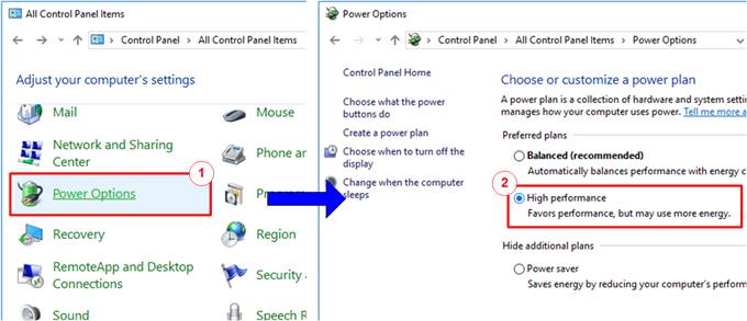
Figure 3‑4 Power options
3.4 Firewall Setting
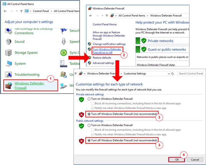
Figure 3‑5 Firewall setting
1) Open Control Panel and select Windows Firewall.
2) Click “Turn Windows Firewall on or off”.
3) Select Turn off Firewall under Private and Public network settings.
4) Click OK button to confirm the setting.
4 FPGA board setup
1) Power off system.
2) Connect micro USB cable from FPGA board to PC for JTAG programming and JTAG UART.
3) Connect QSFP AOC between FPGA board and PC for 40Gb ethernet connection.
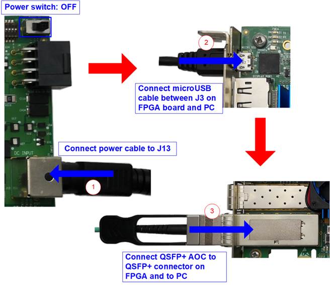
Figure 4‑1 Power cable, microUSB cable, and QSFP+ cable
4) Power on FPGA board.
5) Open QuartusII Programmer to program FPGA through USB-1 by following step.
a) Click “Hardware Setup…” to select USB-BlasterII[USB-1].
b) Click “Auto Detect” and select FPGA (10AS066N3).
c) Select A10 device icon
d) Click “Change File” button, select SOF file in pop-up window, and click “open” button
e) Check “program”
f) Click “Start” button to program FPGA
g) Wait until Progress status is equal to 100%
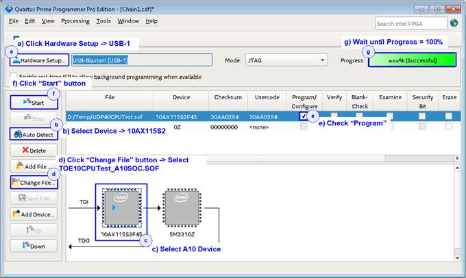
Figure 4‑2 FPGA Programmer
6) Open NiosII command shell and type “nios2-terminal” to run the application.
7) Input ‘0’ to initialize UDP40G-IP in client mode (ask PC MAC address by sending ARP request).
8) Default parameter in client mode is displayed on the console.
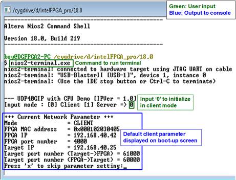
Figure 4‑2 Message after system boot-up
9) User inputs ‘x’ to skip parameter setting and use default parameters for system initialization, as shown in Figure 4‑3. Otherwise, the menu to change parameter is displayed. The example to change parameter is described in topic 5.2.

Figure 4‑3 Initialization complete
Note: Transfer performance in the demo depends on Test PC resource in Test platform.
5 Main menu
5.1 Display current parameter
Select ‘0’ to check current parameter in the demo. There are seven parameters displayed on the console.
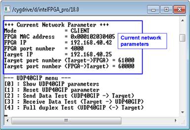
Figure 5‑1 Display current parameter result
1) Mode: Set mode to initialize UDP40G-IP as server or client. To run with PC, please input ‘0’ to initialize UDP40G-IP as client mode.
2) FPGA MAC address: 48-bit hex value to be MAC address of FPGA. Default value is 0x000102030405.
3) FPGA IP: IP address of FPGA. Default value is 192.168.40.42.
Note: This value is used to be FPGA IP address, parameter for test application on PC.
4) Target IP: IP address of destination device (40 Gb Ethernet card on PC). Default value is 192.168.40.25.
5) FPGA port number: Port number of FPGA. Default value is 4000.
Note: This value is used to be FPGA port, parameter for test application on PC.
6) Target port number (Target->FPGA): Port number of the destination device to send data to FPGA. Default value is 61000.
Note: This value is used to be PC port, parameter for test application on PC in transmit mode.
7) Target port number (FPGA->Target): Port number of the destination device to receive data from FPGA. Default value is 60000.
Note: This value is used to be PC port, parameter for test application on PC in received mode.
To change some parameters, user can change by using menu [1] (Reset UDP40GIP parameter).
5.2 Reset UDP40G-IP
Select ‘1’ to reset the IP with or without changing IP parameters.
This menu is used to send reset to UDP40G-IP for loading the latest parameters which may be updated in this menu. After user selects this menu, the current parameters are displayed on the console. User enters ‘x’ to use same parameters and asserts reset to UDP40G-IP. Other keys are input to change some parameters and then asserts reset to UDP40G-IP.
There are seven parameters to set in this menu. After user sets each parameter, CPU validates the value. The parameter is updated to UDP40G-IP when the input is valid. If the input is not valid, the same value still be used. After finishing parameter setting, IP is reset to start IP initialization. The description of each parameter is shown in topic 5.1 (Display current parameter) and the range of each parameter is described as follows.
1) Mode: ‘0’ to initialize as client mode.
2) FPGA MAC address: 12-digit of hex value. Add “0x” as a prefix to input as hex value.
3) FPGA IP address: A set of four decimal digits is separated by “.”. The valid range of each decimal digit is 0-255.
4) Target IP address: A set of four decimal digits like FPGA IP address. This value is IP address of Test PC.
5) FPGA port number: Valid range is 0-65535.
6) Target port number (Target->FPGA): Valid range is 0-65535.
7) Target port number (FPGA->Target): Valid range is 0-65535.
After finishing parameter assignment, new parameters are displayed on the console. Next, reset signal is sent to the IP to initialize system by using the new parameters. Finally, “IP initialization complete” is displayed after IP finishes initialization process, as shown in Figure 5‑2.
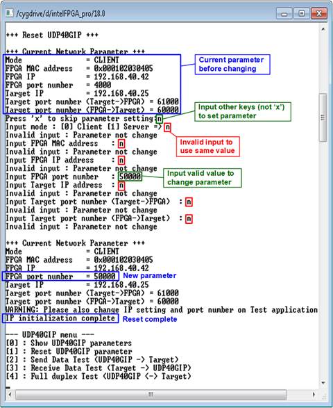
Figure 5‑2 Change IP parameter result
5.3 Send Data Test
To send data from FPGA to PC, select ‘2’ to run send data test on FPGA and prepare “udpdatatest.exe” on PC to receive data. User sets test parameters on FPGA for sending data through NiosII command shell. On PC, user sets test parameters of “udpdatatest” to receive data through Command prompt. The step to run the test is described as follows.
1) On NiosII command shell, set two parameters under send data test menu.
a) Input transfer size: Unit of transfer size is byte. Valid value is 32- 0xFFFF_FFFF_FFE0. The value must be aligned to 32. The input is decimal unit when the input is only digit number. User can add “0x” as a prefix for hexadecimal input.
b) Input packet size: Unit of packet size is byte. Valid value is 32 – 8960. The value must be aligned to 32. The input is decimal unit when the input is only digit number. User can add “0x” as a prefix for hexadecimal input.
Note: When packet size is more than 1472, the packet output from UDP40G-IP is jumbo frame. In this case, Test PC must support jumbo frame.
2) When all inputs are valid, the recommended parameters to run test application on PC are displayed. Next, “Press any key to start data sending ...” is displayed to wait until user enters any key(s) to start the operation.
3) On Command prompt, user runs application by using the recommended parameters. There are seven parameters for “udpdatatest”.
>> udpdatatest [Dir] [FPGA IP] [FPGA Port] [PC Port] [Bytelen] <Pattern> <Timeout>
a) Dir: Set ‘r’ to receive and verify test data from FPGA
b) FPGA IP: Set same value as FPGA IP address
c) FPGA port: Set same value as FPGA port number
d) PC port: Set same value as target port number (FPGA->Target)
e) Bytelen: Set same value as “Input transfer size” of step 1a)
f) Pattern: ‘1’-enable data verification, ‘0’-disable data verification. To use default value (‘1’), this input is not necessary.
g) Timeout: Timeout in msec unit. Valid value is 100-65536. To use default value (100 msec), this input is not necessary.
4) After running test application, some parameters are displayed. After that, PC waits until the data is received from FPGA.
5) On NiosII command shell, user enters any key(s) to start sending data. During transferring data, current transfer size is displayed on NiosII command shell (transmit size) and Command prompt (received size) every second.
6) “Send data complete” is displayed on NiosII command shell after all data are sent. On PC, test application is completed when total data are received or timeout is found. Timeout message with the 1st error position is displayed when test application is finished by timeout condition. Finally, total transfer size and performance are displayed on NiosII command shell (transmit performance) and Command prompt (received performance).
Figure 5‑3 and Figure 5‑4 show the example of Send data test by using small data size and enable data verification on PC test application. When running small size, test application can process all received data in time. Total time usage for small size is too less, so the test application cannot show the correct performance. The performance result can be calculated and displayed on NiosII command shell. Running small data size cannot show the different performance between using jumbo frame and non-jumbo frame. Typically, using jumbo frame shows the better performance than using non-jumbo frame.
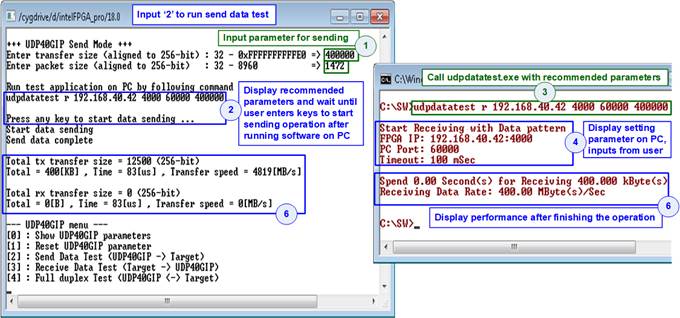
Figure 5‑3 Send data test by using non-jumbo frame without lost data
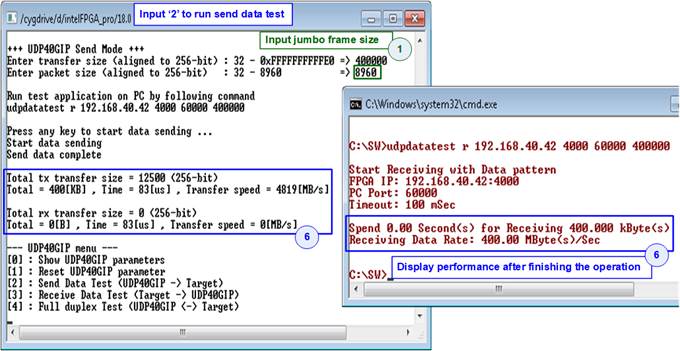
Figure 5‑4 Send data test by using jumbo frame without lost data
Figure 5‑5 and Figure 5‑6 show the example of Send data test when transferring 34 GB data with and without data verification on PC. It is found that the test application cannot process the received data in time though it runs without data verification. There are many lost data when transferring data from FPGA to PC. On PC, total received size with enable data verification is about 12 GB (12/34 = 35%) while total received size without data verification is about 16 GB (16/34 = 47%). So, the performance displayed on PC is less than the performance displayed on NiosII command shell, following the total data size. The performance is reduced from PC resource limitation.
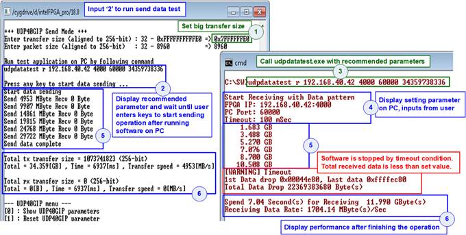
Figure 5‑5 Send data test with data verification with lost data

Figure 5‑6 Send data test without data verification when lost data
When the input is invalid, “Out-of-range input”/”Invalid input” is displayed and the operation is cancelled, as shown in Figure 5‑7 - Figure 5‑8.
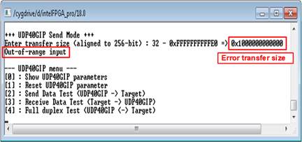
Figure 5‑7 Error from invalid transfer size
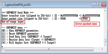
Figure 5‑8 Error from invalid packet size
5.4 Receive Data Test
To transfer data from PC to FPGA, select ‘3’ to run receive data test on FPGA and prepare “udpdatatest” on PC to send data. User sets test parameters on FPGA for receiving data through NiosII command shell. On PC, user sets test parameters of “udpdatatest” to send data through Command prompt. The step to run the test is described as follows.
1) On NiosII command shell, set two parameters under receive data test menu.
a) Input transfer size: Unit of transfer size is byte. Valid value is 32- 0xFFFF_FFFF_FFE0. The value must be aligned to 32. The input is decimal unit when the input is only digit number. User can add “0x” as a prefix for hexadecimal input.
b) Input data verification mode: ‘0’-disable data verification, ‘1’-enable data verification sent from PC.
2) When all inputs are valid, the recommended parameters to run test application on PC are displayed. After that, “Wait data from Target ...” is displayed and IP is ready to receive data from PC.
3) On Command prompt, user runs application by using the recommended parameters. There are seven parameters for “udpdatatest”.
>> udpdatatest [Dir] [FPGA IP] [FPGA Port] [PC Port] [Bytelen] <Pattern> <Timeout>
a) Dir: Set ‘t’ to send test data from FPGA
b) FPGA IP: Set same value as FPGA IP address
c) FPGA port: Set same value as FPGA port number
d) PC port: Set same value as target port number (Target->FPGA)
e) Bytelen: Set same value as “Input transfer size” of step 1a)
f) Pattern: Set same value as “Input data verification mode” of step 1b). To use default value ‘1’, this input is not necessary.
g) Timeout: This input is not used in transmit mode.
4) After running test application, test application starts sending data to FPGA. During transferring data, current transfer size is displayed on both NiosII command shell (received size) and Command prompt (transmit size) every second.
5) “Receive data completed” is displayed on NiosII command shell after FPGA receives all data or timeout is found. Finally, total transfer size and performance are displayed on NiosII command shell (received performance) and Command prompt (transmit performance).
Figure 5‑9 and Figure 5‑10 show the example of receive data test when disable and enable data verification mode on FPGA. The application generates dummy data or incremental data, depending on Pattern parameter. The left window is test result on NiosII command shell while the right window is test result on Command prompt.
The performance depends on PC resource limitation. The performance when running dummy data is better than incremental data which uses much PC resource.
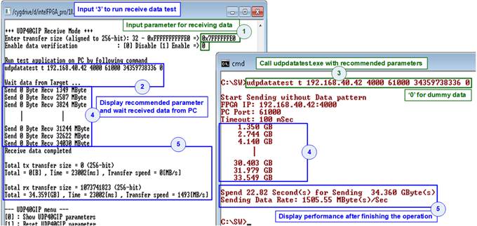
Figure 5‑9 Receive data test when disable data verification

Figure 5‑10 Receive data test when enable data verification
Figure 5‑11 shows the example of error when data verification is failed. In the example, the error is caused from mismatch verification mode value. FPGA enables data verification while “udpdatatest” sends dummy data. The error message is displayed on NiosII command shell.
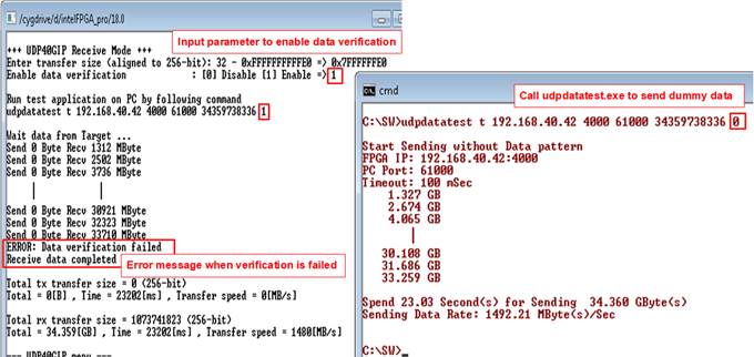
Figure 5‑11 Receive data test when data verification is failed
5.5 Full-duplex Test
Select ‘4’ to run full-duplex test to transfer data between FPGA and PC in both directions at the same time. User sets test parameters on FPGA through NiosII command shell and test parameters on PC through Command prompt. Two “udpdatatest” applications are called through two Command prompts to send data and receive data by using different port number. The step to run the test is described as follows.
1) On NiosII command shell, set three parameters under full-duplex test menu.
a) Input transfer size: Unit of transfer size is byte. Valid value is 32 - 0xFFFF_FFFF_FFE0. The value must be aligned to 32. The input is decimal unit when the input is only digit number. User can add “0x” as a prefix for hexadecimal input.
b) Input packet size: Unit of packet size is byte. Valid value is 32 – 8960. The value must be aligned to 32. The input is decimal unit when the input is only digit number. User can add “0x” as a prefix for hexadecimal unit.
c) Input data verification mode: ‘0’-disable data verification, ‘1’-enable data verification.
2) When all inputs are valid, the recommended parameters to run two test applications on PC are displayed. First parameter is for sending data test and another parameter is for receiving data test. Next, “Press any key to start data sending ...” is displayed to wait user starting the operation on NiosII command shell.
3) On PC, open two Command prompts and run the application by using the recommended value. There are seven parameters for “udpdatatest”.
>> udpdatatest [Dir] [FPGA IP] [FPGA Port] [PC Port] [Bytelen] <Pattern> <Timeout>
a) Dir: Set ‘r’ to the 1st Command prompt.
Set ‘t’ to the 2nd Command prompt.
b) FPGA IP: Set same value as FPGA IP address
c) FPGA port: Set same value as FPGA port number
d) PC port: Set same value as target port number (FPGA->Target) to the 1st Command prompt. Set same value as target port number (Target->FPGA) to the 2nd Command prompt.
e) Bytelen: Set same value as “Input transfer size” of step 1a)
f) Pattern: Set same value as “Input data verification mode” of step 1b) to the 1st Command prompt. Set ‘1’-enable or ‘0’-disable data verification for the 2nd Command prompt. Default value is ‘1’.
g) Timeout: Timeout in msec unit. Valid value is 100-65536. To use default value (100 msec), this input is not necessary.
4) On NiosII command shell, user enters any key(s) to start sending data to PC. Current transfer size in both directions is displayed on NiosII command shell and two Command prompts every second.
5) “Transfer data complete” is displayed on NiosII command shell after UDP40G-IP finishes the operation for sending and receiving data. Finally, total transfer size and performance are displayed on NiosII command shell and Command prompt.
Figure 5‑12 and Figure 5‑13 show the example to run full-duplex with data verification by using small size and big size. The left window is the test result on NiosII command shell while the right window is the test result on Command prompt (the upper window is received mode and the lower window is transmit mode). When transfer size is less, there is no lost data. The lost data is found with error message when transfer size is big. Similar to send and receive data test, the performance depends on PC resource limitation.
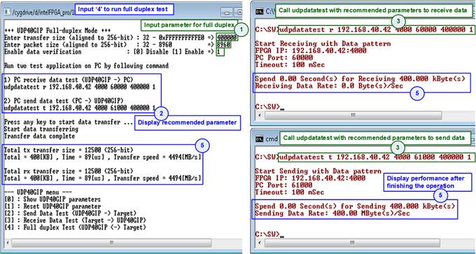
Figure 5‑12 Full-duplex test without lost data
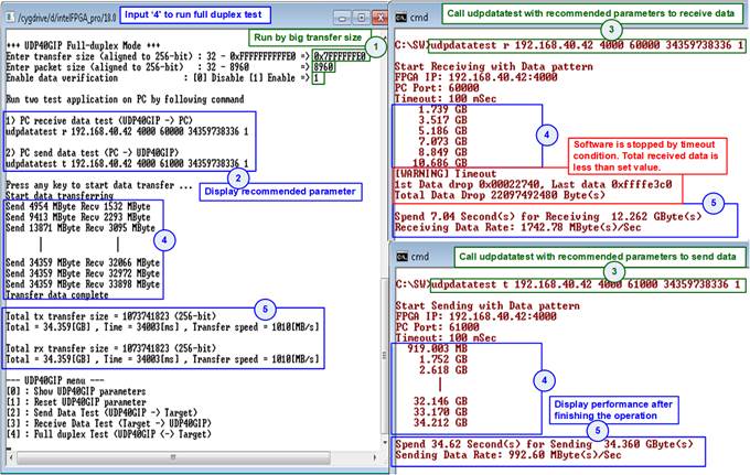
Figure 5‑13 Full-duplex test with lost data
Part B UDP40G-IP demo by using two FPGAs
6 Environment Setup
To run UDP40G-IP by using two FPGAs as shown in Figure 6‑1, please prepare the following test environment.
1) Two FPGA development boards (Arria10 GX development kit)
2) QSFP+ AOC for 40G ethernet connection between two FPGA boards
3) micro USB cable for programming FPGA and NiosII terminal between FPGA board and PC. Two cables are used for two FPGA boards.
4) QuartusII programmer for programming FPGA and NiosII command shell, installed on PC
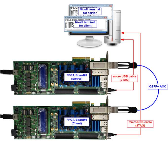
Figure 6‑1 UDP40G-IP demo (FPGA<->FPGA) by Arria10 GX board
7 FPGA board setup
Please follow topic 4 (FPGA board setup) to prepare FPGA board and QSFP+ AOC connection for running the demo. When connecting two FPGA boards to one PC, two USB-BlasterII are detected as USB-1 and USB-2. User must select the correct USB channel to configure FPGA and run NiosII command shell for two FPGAs, as shown in the following example.
1) When connecting two FPGA boards to one PC, two USB-Blasters are detected as USB-1 and USB-2. Select hardware setup to USB-1 and configure FPGA board#1 until finishing. After that, change hardware setup to USB-2 and configure FPGA board#2 until finishing.

Figure 7‑1 Select USB-Blaster cable for FPGA configuration
2) Open NiosII command shell to connect with FPGA board#1 and FPGA board#2.
a) Type “nios2-terminal -- cable 1” to open NiosII terminal of FPGA board#1 (USB-1 port)
b) Type “nios2-terminal -- cable 2” to open NiosII terminal of FPGA board#2 (USB-2 port)
c) Set ‘1’ on NiosII terminal of FPGA board#1 for running server mode and set ‘0’ on NiosII terminal of FPGA board#2 for running client mode.

Figure 7‑2 Open NiosII terminal on two FPGA boards
3) Default parameters are displayed on NiosII command shell of board#1 and board#2. Please setup parameters of server mode before client mode.
a) After setting ‘1’ on NiosII command shell of board#1 for running server mode, enter ‘x’ to skip parameter setting and run test system by using default parameters, as shown in Figure 7‑3.
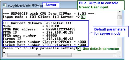
Figure 7‑3 Use default parameter in server mode
b) Set ‘0’ on Serial console of board#2 for running client mode. After that, user must change target port number (Target->FPGA) to use same value as target port number (FPGA->Target), as shown in Figure 7‑4.
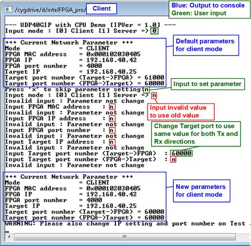
Figure 7‑4 Modify parameter in client mode
Note: Please complete to setup parameter and reset process on server before client. Server must be reset to start IP initialization by waiting ARP request from client.
4) After finishing setting parameters, IP starts initialization process. “IP initialization complete” is displayed when finishing the initialization process. Finally, main menu is displayed on both NiosII command shells.

Figure 7‑5 Display main menu
8 Main menu
8.1 Display current parameter
Select ‘0’ to check current parameter in the demo. There are seven parameters displayed on NiosII command shell.
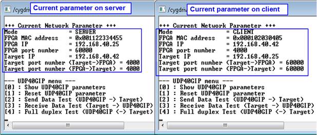
Figure 8‑1 Display current parameter result
1) Mode: Set mode to initialize UDP40G-IP as server or client (‘0’: Client, ‘1’: Server).
2) FPGA MAC address: 48-bit hex value to be MAC address of FPGA. Default value is 0x000102030405 (client mode) or 0x001122334455 (server mode).
3) FPGA IP: IP address of FPGA. Default value is 192.168.40.42 (client mode) or 192.168.40.25 (server mode).
4) Target IP: IP address of destination device. Default value is 192.168.40.25 (client mode) or 192.168.40.42 (server mode).
5) FPGA port number: Port number of FPGA. Default value is 4000 (client mode) or 60000 (server mode).
6) Target port number (Target->FPGA): Port number of the destination device to send data to UDP40G-IP. Default value is 61000 (client mode) or 4000 (server mode). In client mode, this value must be changed from 61000 to 60000 (same as default value of Target port number for FPGA -> Target).
7) Target port number (FPGA->Target): Port number of the destination device to receive data from UDP40G-IP. Default value is 60000 (client mode) or 4000 (server mode).
To change some parameters, user can change by using menu [1] (Reset UDP40GIP parameter).
8.2 Reset UDP40G-IP
Select ‘1’ to reset the IP with or without changing IP parameters.
This menu is used to send reset to UDP40G-IP for loading the latest parameters which may be updated in this menu. After user selects this menu, the current parameters are displayed on the console. User enters ‘x’ to use same parameters and asserts reset to UDP40G-IP. Other keys are input to change some parameters and then asserts reset to UDP40G-IP.
There are seven parameters to set in this menu. After user sets each parameter, CPU validates the value. The parameter is updated to UDP40G-IP when the input is valid. If the input is not valid, the same value still be used. After finishing parameter setting, IP is reset to start IP initialization. The description of each parameter is shown in topic 8.1 (Display current parameter) and the range of each parameter is described as follows.
Note:
1. To change and reset parameters on the server, the client FPGA must be also reset. Server must be reset before client to wait ARP request sent from client.
2. Target port number for sending and receiving data must be same value.
3. Parameter of client and server must be matched.
a. Target IP of server = FPGA IP of client
b. FPGA IP of server = Target IP of client
c. Target port number of server (both Tx and Rx direction) = FPGA port number of client
d. FPGA port number of server = Target port number of client (both Tx and Rx direction)
1) Mode: ‘0’ (client) or ‘1’ (server) for setting FPGA initialization mode. It needs to set different mode for two FPGA boards (one board is client and another board is server).
2) FPGA MAC address: 12-digit of hex value. Add “0x” as a prefix to input as hex value.
3) FPGA IP address: A set of four decimal digits is separated by “.”. The valid range of decimal digit is 0-255.
4) Target IP address: A set of four decimals like FPGA IP address.
5) FPGA port number: Valid range is 0-65535.
6) Target port number (Target->FPGA): Valid range is 0-65535.
7) Target port number (FPGA->Target): Valid range is 0-65535.
After finishing parameter assignment, new parameters are displayed on the console. Next, reset signal is sent to the IP to initialize system by using the new parameters. Finally, “IP initialization complete” is displayed after IP finishes initialization process, as shown in Figure 8‑2.

Figure 8‑2 Change IP parameter result
8.3 Send and Receive data Test (Half-duplex test)
The steps to send and receive data test on server and client mode are similar. So, this topic describes the menu to transfer data between two FPGA boards. The 1st board runs receive data test (select menu ‘3’) while another board runs send data test (select menu ‘2’).
User sets test parameters through NiosII command shell. The step to run the test is described as follows.
1) On NiosII command shell under menu 3 (receive data test), set two parameters.
a) Input transfer size: Unit of transfer size is byte. Valid value is 32- 0xFFFF_FFFF_FFE0. The value must be aligned to 32. The input is decimal unit when the input is only digit number. User can add “0x” as a prefix for hexadecimal input.
b) Input data verification mode: ‘0’-disable data verification, ‘1’-enable data verification.
2) When all inputs are valid, “Wait data from Target ...” is displayed.
3) On NiosII command shell under menu 2 (send data test), set two parameters.
a) Input transfer size: Unit of transfer size is byte. Valid value is 32- 0xFFFF_FFFF_FFE0. The value must be aligned to 32. The input is decimal unit when the input is only digit number. User can add “0x” as a prefix for hexadecimal unit. This input must be the same value as transfer size input under receive data test (step 1a).
b) Input packet size: Unit of packet size is byte. Valid value is 32 – 8960. The value must be aligned to 32. The input is decimal unit when the input is only digit number. User can add “0x” as a prefix for hexadecimal input.
4) When all inputs are valid, “Press any key to start data sending ...” is displayed. User enters some key(s) to start sending data.
5) During transferring data, current transfer size is displayed on both NiosII command shells every second.
6) “Send data complete” and “Receive data completed” are displayed on NiosII command shell after finishing the operation. Finally, total transfer size and performance are displayed on both NiosII command shell.
Figure 8‑3 and Figure 8‑4 show the example to transfer data between two FPGAs by using non-jumbo frame size and jumbo frame size. The left window is NiosII command shell from FPGA running receive data test while the right window is NiosII command shell from FPGA running send data test. The performance output when using jumbo frame is slightly better than non-jumbo frame.
When some inputs are invalid, “Out-of-range input”/”Invalid input” is displayed and the operation is cancelled, as shown in Figure 5‑7 - Figure 5‑8 (same as FPGA<->PC test).
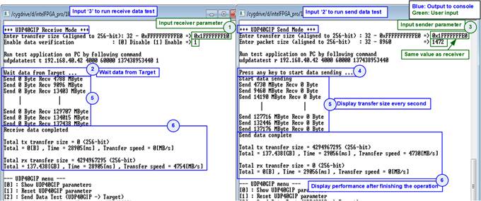
Figure 8‑3 Send/receive data test by using non-jumbo frame

Figure 8‑4 Send/receive data test by using jumbo frame
8.4 Full-duplex Test
Select ‘4’ to run full-duplex test on two FPGAs to transfer data in both directions at the same time and same port number. User sets test parameters through NiosII command shell. User must start the operation on the server before the client. The step to run the test is described as follows.
1) On server NiosII command shell, set three parameters under full-duplex test menu.
a) Input transfer size: Unit of transfer size is byte. Valid value is 32 - 0xFFFF_FFFF_FFE0. The value must be aligned to 32. The input is decimal unit when the input is only digit number. User can add “0x” as a prefix for hexadecimal unit.
b) Input packet size: Unit of packet size is byte. Valid value is 32 – 8960. The value must be aligned to 32. The input is decimal unit when the input is only digit number. User can add “0x” as a prefix for hexadecimal unit.
a) Input data verification mode: ‘0’-disable data verification, ‘1’-enable data verification.
2) When all inputs are valid, “Wait data from Target …” is displayed.
3) On client NiosII command shell, set three parameters under full-duplex test menu.
a) Input transfer size: Unit of transfer size is byte. Valid value is 32 - 0xFFFF_FFFF_FFE0. The value must be aligned to 32. The input is decimal unit when the input is only digit number. User can add “0x” as a prefix for hexadecimal unit. This input must be same value as transfer size input of server FPGA (step 1a).
b) Input packet size: Unit of packet size is byte. Valid value is 32 – 8960. The value must be aligned to 32. The input is decimal unit when the input is only digit number. User can add “0x” as a prefix for hexadecimal unit.
c) Input data verification mode: ‘0’-disable data verification, ‘1’-enable data verification.
4) When all inputs are valid, “Press any key to start data transfer ...” is displayed. User enters some keys to start full-duplex test.
5) During transferring data, current transfer size is displayed on both NiosII command shells every second.
6) “Transfer data complete” is displayed on both NiosII command shells. Finally, total transfer size and performance are displayed on both NiosII command shells.
Figure 8‑5 and Figure 8‑6 shows full-duplex test when running by using non-jumbo frame and jumbo frame size. The left window is NiosII command shell from server FPGA while the right window is NiosII command shell from client FPGA. Using jumbo frame size shows the better performance than using non-jumbo frame. Data verification by the hardware does not have any effect to the performance, so the user can enable data verification in the test.
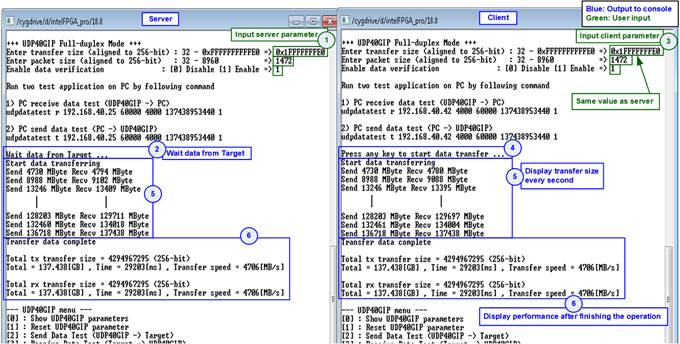
Figure 8‑5 Full-duplex test when using non-jumbo frame

Figure 8‑6 Full-duplex test when using jumbo frame
9 Revision History
|
Revision |
Date |
Description |
|
1.0 |
28-Oct-19 |
Initial version release |