Rev1.0 12-Jul-23
2.1 Low Latency 40G Ethernet IP
3 CPU Firmware Sequence (FPGA)
3.6 Function list in User application
1 Introduction
Comparing to TCP protocol, UDP protocol provides a procedure to send data with a minimum of protocol mechanism, but the data cannot guarantee to be accepted by the destination because of no handshaking dialogues providing in UDP mechanism. Similar to TCP protocol, UDP protocol provides checksums for data integrity and port numbers for addressing different functions at the source and the destination in the communication networks.
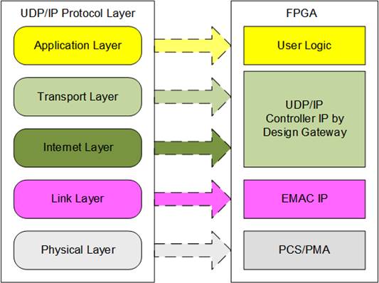
Figure 1‑1 UDP/IP Protocol Layer
UDP40G-IP implements Transport and Internet layer of UDP/IP model. To send data, UDP40G-IP prepares UDP data from user logic, adds UDP/IP header to generate Ethernet packet, and sends to EMAC. To receive data, UDP40G-IP extracts UDP data and header from Ethernet packet. When UDP/IP header in the packet is valid, UDP data is stored to the buffer for user logic reading.
The lower layer protocols are implemented by 40Gb Ethernet MAC IP and PHY IP. In the reference design, both IPs are the IP core from Intel FPGA.
This reference design provides evaluation system which includes simple user logic to send and receive data by using UDP40G-IP. For user interface, CPU system is designed to interface with user through JTAG UART. The firmware is designed as bare-metal OS (no operating system). The test application software (“udpdatatest.exe”), run on PC, is also designed for sending and receiving UDP/IP packet with UDP40G-IP. The reference design is available on Intel FPGA development board to show ultra-speed data transferring. More details of the demo are described as follows.
2 Hardware design
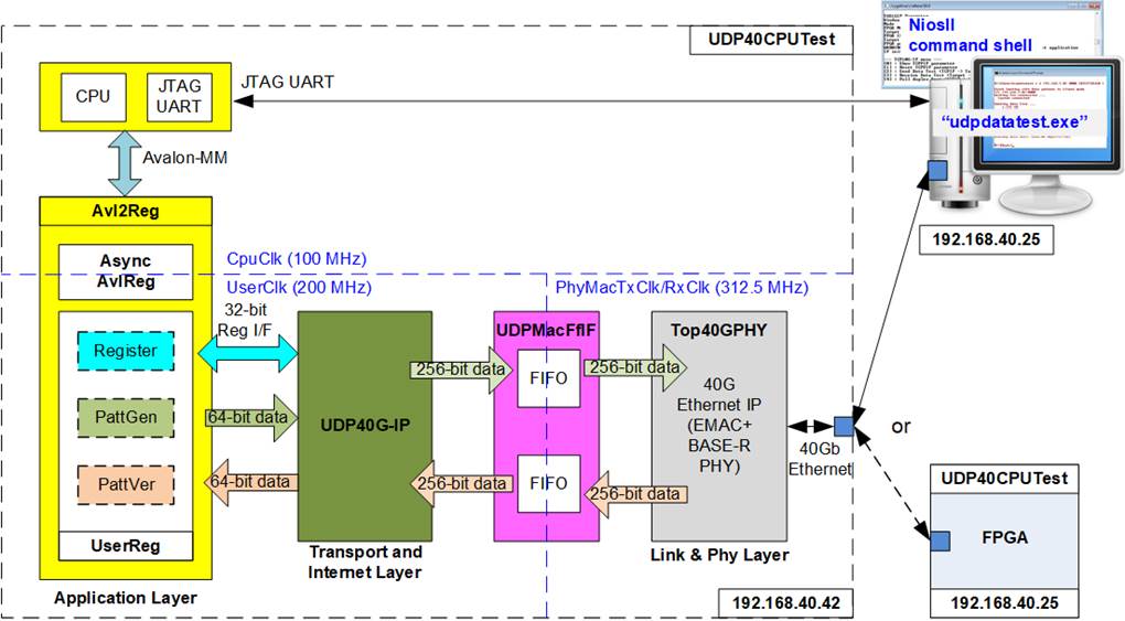
Figure 2‑1 Demo block diagram
In test environment, two devices are used for 40Gb Ethernet transferring. This reference design is designed to run under two test environments. First is one FPGA including UDP40G-IP transferring UDP packet with one PC running “udpdatatest.exe”. Second is two FPGAs transferring UDP packet each other. Running with PC can confirm the compatibility of UDP40G-IP with general system while two FPGA boards are applied to check the best performance of UDP40G-IP.
In FPGA logic, UDP40G-IP and 40Gb Ethernet MAC and PHY (Intel FPGA IP) are applied to complete all UDP/IP layer implementation. UDPMacFfIF module is used to convert 256-bit FIFO interface of UDP40G-IP to be 40G EMAC interface. User interface of UDP40G-IP is connected to UserReg module within Avl2Reg.
UserReg is designed to connect with user interface of UDP40G-IP for both register interface and data interface. Register files within UserReg are stored test parameters within UserReg. Besides, register signals are applied to control UDP40G-IP. Test pattern, generated by PattGen and PattVer for sending and verifiying data with UDP40G-IP, is 32-bit incremental pattern.
Test parameters are received from user through JTAG UART. The parameters are configured to the hardware through Avalon-MM bus. Due to the fact that CPU system and UDP40G-IP operate in the different clock domain, AsyncAvlReg module must be designed to be asynchronous circuit for clock-crossing operation and converting Avalon-MM bus to be register interface.
CPU firmware designs the test application to transfer data in half-duplex mode for both transfer directions and full-duplex mode. When running with PC, PC must run “udpdatatest.exe” to transfer UDP data with FPGA. One “udpdatatest.exe” is called to send or receive data with FPGA in half-duplex mode while two “udpdatatest.exe” are called to send and receive data with FPGA at the same time by using different port number in full-duplex mode.
CPU system in the reference design is included to allow user running the test under many test parameters and test conditions. In the real application, CPU system can be removed and replaced by the simple logic to set the fixed parameters to UDP40G-IP.
2.1 Low Latency 40G Ethernet IP
This module consists of two submodules, i.e. 40G Ethernet MAC and 40G PCS/PMA in BASE-R mode. In the reference design, it uses 40G Ethernet system, provided by Intel FPGA. The data interface is 256-bit Avalon-Stream. More details of Low Latency 40G Ethernet Intel FPGA IP are described in following link.
https://www.intel.com/content/dam/www/programmable/us/en/pdfs/literature/ug/ug_ll_40gbe.pdf
2.2 UDPMacFfIF
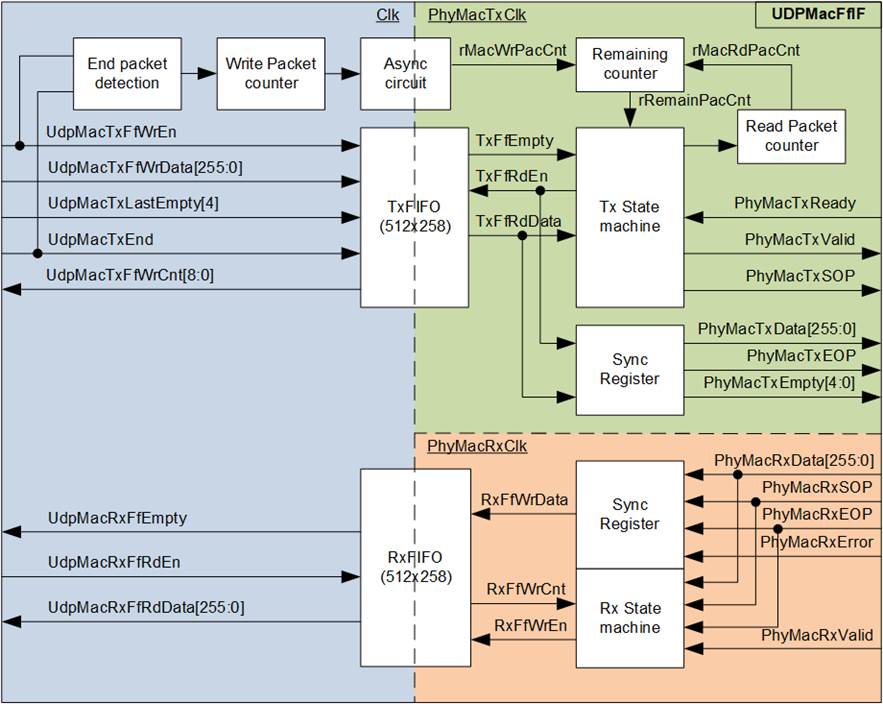
Figure 2‑2 UDPMacFfIF block diagram
This module is designed to be adapter logic connecting between UDP40G-IP and 40G Ethernet MAC. There are three clock domains in this module, i.e. Clk which is synchronous to UDP40G-IP, PhyMacTxClk which is synchronous to Tx interface of 40G EMAC, and PhyMacRxClk which is synchronous to Rx interface of 40G EMAC. The data interface of UDP40G-IP for Tx and Rx direction is 256-bit FIFO interface in ShowAhead mode while the interface of 40G EMAC is 256-bit Avalon-stream interface. Also, the data stream characteristic of UDP40G-IP is continuous for transferring one packet while the data stream of 40G EMAC is transferred one clock every two clock cycles.
UDPMacFfIF is designed for three features, i.e. converting interface type, adding asynchronous circuit for clock-crossing domain, and including the buffer for supporting different data stream characteristic. To implement these features, two asynchronous ShowAhead FIFOs must be implemented in UDPMacFfIF (one for Tx interface and another for Rx interface). The maximum size of UDP packet on the current Ethernet system is less than 9K byte, so FIFO size is set to 512x258-bit for storing at least one packet. The adapter logic is independently designed for each transfer direction.
For Tx interface, write interface of TxFIFO is connected to UDP40G-IP directly. The logic to count total Tx packet stored in UDPMacFfIF is designed, called Write packet counter. The counter is increased when end of Tx packet is detected and then forwarded to PhyMacTxClk domain through asynchronous circuit. Read interface of TxFIFO is controlled by Tx state machine. When at least one Tx packet is ready inside TxFIFO, Tx state machine forwards all data of one packet from TxFIFO to 40G EMAC following Avalon-stream standard. Similar to Write packet counter, there is the counter to count total read packet from TxFIFO which is counted when the 1st data in each packet is sent. So, Tx state machine can calculate the remaining packet counter (rRemainPacCnt) in TxFIFO by calculating the different value of write counter and read counter.
To reduce data bus size of TxFIFO, only bit 4 of TxLastEmpty signal from UDP40G-IP is applied because TxLastEmpty, output from UDP40G-IP, can be equal to two values, i.e. 0x16 and 0x04.
Timing diagram of the logic to read data from TxFIFO and forward to 40G EMAC is shown in Figure 2‑3.
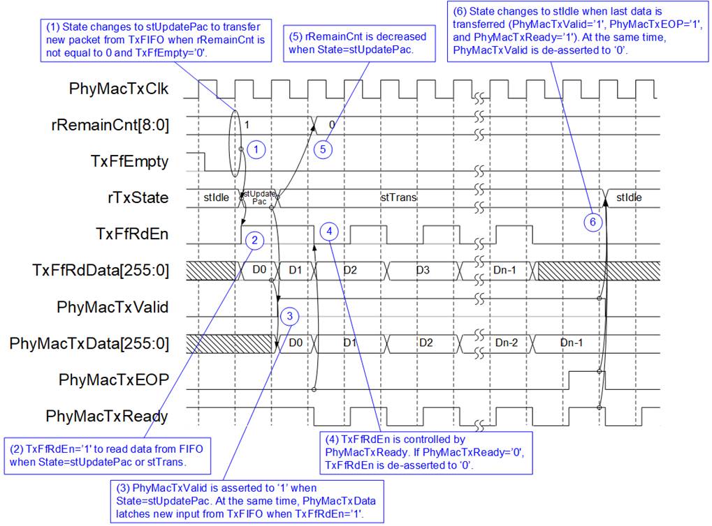
Figure 2‑3 PhyMacTx interface timing diagram
When at least one packet is available in TxFIFO (rRemainCnt is not equal to 0 and TxFfEmpty is equal to ‘0’), TxState starts forwarding one packet from TxFIFO to 40G EMAC by changing state from stIdle to stUpdatePac. stUpdatePac is run only one clock cycle to decrease rRemainCnt signal. In this clock, the 1st data is read from TxFIFO.
In the next clock, TxState changes to stTrans. TxFfRdEn still be asserted to ‘1’ to read data from TxFIFO when 40G EMAC is ready to receive data (PhyMacTxReady=’1’). TxFfRdEn is also applied as latch enable of PhyMacTxData which holds the data output from TxFIFO for forwarding to 40G EMAC. At the same time, PhyMacTxValid is always asserted to ‘1’ to send valid data to 40G EMAC until end of packet.
During packet transferring, PhyMacTxReady could be de-asserted to ‘0’ to pause data transmission when 40G EMAC is not ready. TxFfRdEn is de-asserted to ‘0’ to hold the same data on PhyMacTxData signal, following PhyMacTxReady signal. After end of packet is transferred (PhyMacTxEOP=’1’), state machine changes from stTrans to stIdle and PhyMacTxValid is de-asserted to ‘0’ to finish transferring one packet.
Similar to Tx direction, read interface of RxFIFO is connected to UDP40G-IP directly. Rx state machine checks free space of RxFIFO by monitoring RxFfWrCnt. When free space is more than 9 Kbyte, the received packet from 40G EMAC is stored to RxFIFO. Otherwise, the received packet is dropped.
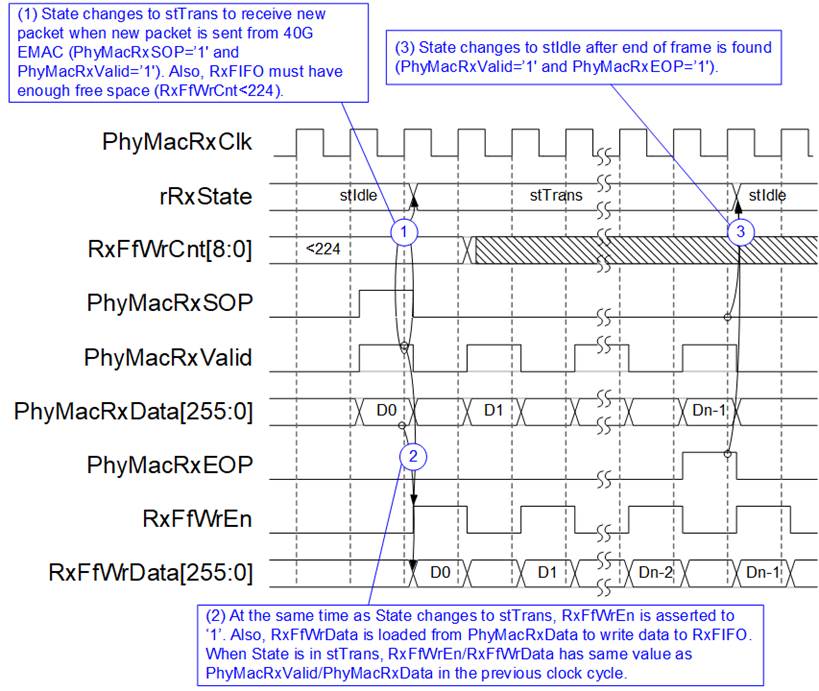
Figure 2‑4 PhyMacRx interface timing diagram when RxFIFO is ready
When new packet is received from 40G EMAC, Rx state machine confirms that RxFfWrCnt (RxFIFO write counter) has free space enough to store 9Kbyte packet by comparing to 224 (Free space = (511 – 224) x 32 = 9184 byte). In stTrans, data from 40G EMAC (PhyMacRxData) is stored to RxFIFO by asserting RxFfWrEn to ‘1’ following PhyMacRxValid. RxFfWrData is one-clock delayed signal of PhyMacRxData to synchronous with RxFfWrEn timing diagram. When end of packet is found (PhyMacRxValid=’1’ and PhyMacRxEOP=’1’), Rx state machine changes to stIdle.
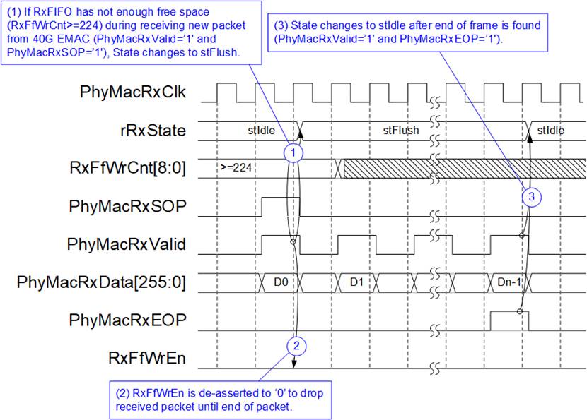
Figure 2‑5 PhyMacRx interface timing diagram when RxFIFO is not ready
Rx state machine changes to stFlush to drop the received packet from 40G EMAC when RxFIFO is full (RxFfWrCnt is more than or equal to 224). RxFfWrEn is de-asserted to ‘0’ until end of the packet (PhyMacRxValid=’1’ and PhyMacRxEOP=’1’). After that, Rx state machine returns to stIdle to process the next packet.
2.3 UDP40G-IP
UDP40G-IP implements UDP/IP stack and offload engine. Control and status signals for user interface are accessed through 32-bit register interface. Data interface is accessed through 256-bit FIFO interface. More details are described in datasheet.
https://dgway.com/products/IP/UDP40G-IP/dg_udp40gip_data_sheet_intel_en.pdf
2.4 CPU and Peripherals
32-bit Avalon-MM bus is the bus interface for CPU accessing the peripherals such as Timer and JTAG UART. To control and monitor the test system, the control and status signals are connected to register for CPU access as a peripheral through 32-bit Avalon-MM bus. CPU assigns the different base address and the address range for each peripheral.
In the reference design, the CPU system is built with one additional peripheral to access the test logic. The base address and the range for accessing the test logic are defined in the CPU system. So, the hardware logic must be designed to support Avalon-MM bus standard for writing and reading the register. Avl2Reg module is designed to connect the CPU system as shown in Figure 2‑6.
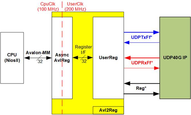
Figure 2‑6 Avl2Reg block diagram
Avl2Reg consists of AsyncAvlReg and UserReg. AsyncAvlReg is designed to convert the Avalon-MM signals to be the simple register interface which is 32-bit data bus size (similar to Avalon-MM data bus size). Additionally, AsyncAvlReg includes asynchronous logic to support clock crossing between CpuClk domain and UserClk domain.
UserReg includes the register file of the parameters and the status signals. Also, data interface and control interface of UDP40G-IP are connected to UserReg. More details of AsyncAvlReg and UserReg are described as follows.
2.4.1 AsyncAvlReg
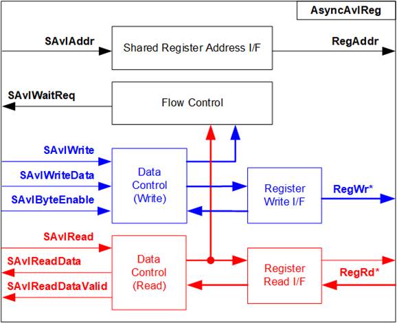
Figure 2‑7 AsyncAvlReg Interface
The signal on Avalon-MM bus interface can be split into three groups, i.e. SAvlWrite* (Write channel), SAvlRead* (Read channel), and SAvlAddr/SAvlWaitReq (Shared control channel). More details of Avalon-MM interface specification are described in following document.
https://www.intel.com/content/dam/www/programmable/us/en/pdfs/literature/manual/mnl_avalon_spec.pdf
According to Avalon-MM specification, one command (write or read) can be operated at a time. SAvlWaitReq is the control signal which is shared between write and read transaction. This signal is asserted to hold the next request from Avalon-MM interface while the current request is operating. In Write access, Write signals of Avalon-MM bus are latched and transferred as Write register. In Read access, Read signals of Avalon-MM bus are latched and transferred as Read register. The address on Avalon-MM is shared signal which is latched and transferred to be Address register interface as well.
The simple register interface is compatible to general RAM interface for write transaction. The read transaction of the register interface is slightly modified from RAM interface by adding RdReq and RdValid signal to control read timing. The address of register interface is shared for write and read transaction. So, user cannot write and read the register at the same time. The timing diagram of the register interface is shown in Figure 2‑8.
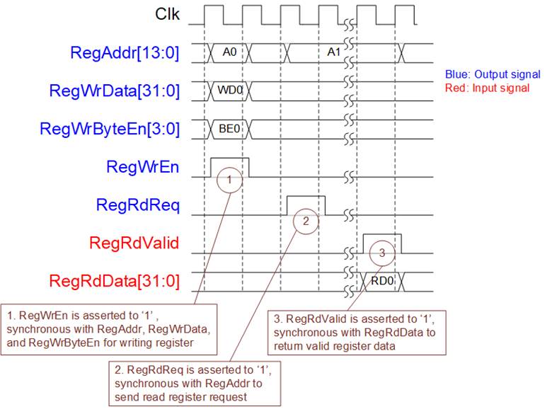
Figure 2‑8 Register interface timing diagram
1) To write register, the timing diagram is the same as general RAM interface. RegWrEn is asserted to ‘1’ with the valid RegAddr (Register address in 32-bit unit), RegWrData (write data of the register), and RegWrByteEn (the write byte enable). Byte enable has four bits to be the byte data valid, i.e. bit[0] for RegWrData[7:0], bit[1] for RegWrData[15:8], and so on.
2) To read register, AsyncAvlReg asserts RegRdReq to ’1’ with the valid RegAddr. 32-bit read data must be returned after receiving the read request. The slave must always monitor RegRdReq signal.
3) When the read data is returned on RegRdData bus, the slave asserts RegRdValid to ‘1’. After that, AsyncAvlReg forwards the read value to SAvlRead* interface.
2.4.2 UserReg
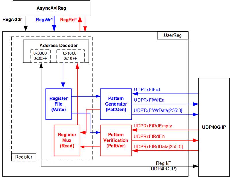
Figure 2‑9 UserReg block diagram
The logic inside UserReg has three parts, i.e. Register block, Pattern generator (PattGen), and Pattern verification (PattVer). Register block decodes the address requested from AsyncAvlReg and then selects the active register for write or read transaction. Pattern generator is designed to send 256-bit test data to UDP40G-IP following FIFO interface standard. Pattern verification is designed to read and verify 256-bit data from UDP40G-IP following FIFO interface standard. More details of each part are described as follows.
Register block
The address range to map to UserReg is split into two areas, i.e. UDP40G-IP register (0x0000-0x00FF) and UserReg register (0x1000-0x10FF).
Address decoder decodes the upper bit of RegAddr for selecting the active hardware. The register file inside UserReg is 32-bit bus size, so write byte enable (RegWrByteEn) is not used. To set the parameters in the hardware, the CPU must use 32-bit pointer to force 32-bit valid value of the write data.
To read register, one multiplexer is designed to select the read data within each address area. The lower bit of RegAddr is applied in each Register area to select the data. Next, the address decoder uses the upper bit to select the read data from each area for returning to CPU. Totally, the latency of read data is equal to one clock cycle, so RegRdValid is created by RegRdValid with asserting one D Flip-flop. More details of the address mapping within UserReg module are shown in Table 2‑1
Table 2‑1 Register map Definition
|
Address |
Register Name |
Description |
|
Wr/Rd |
(Label in the “udp40gtest.c”) |
|
|
BA+0x0000 – BA+0x00FF: UDP40G-IP Register Area More details of each register are described in UDP40G-IP datasheet. |
||
|
BA+0x0000 |
UDP40_RST_REG |
Mapped to RST register within UDP40G-IP |
|
BA+0x0004 |
UDP40_CMD_REG |
Mapped to CMD register within UDP40G-IP |
|
BA+0x0008 |
UDP40_SML_REG |
Mapped to SML register within UDP40G-IP |
|
BA+0x000C |
UDP40_SMH_REG |
Mapped to SMH register within UDP40G-IP |
|
BA+0x0010 |
UDP40_DIP_REG |
Mapped to DIP register within UDP40G-IP |
|
BA+0x0014 |
UDP40_SIP_REG |
Mapped to SIP register within UDP40G-IP |
|
BA+0x0018 |
UDP40_DPN_REG |
Mapped to DPN register within UDP40G-IP |
|
BA+0x001C |
UDP40_SPN_REG |
Mapped to SPN register within UDP40G-IP |
|
BA+0x0020 |
UDP40_TDL_REG |
Mapped to TDL register within UDP40G-IP |
|
BA+0x0024 |
UDP40_TDH_REG |
Mapped to TDH register within UDP40G-IP |
|
BA+0x0028 |
UDP40_TMO_REG |
Mapped to TMO register within UDP40G-IP |
|
BA+0x002C |
UDP40_PKL_REG |
Mapped to PKL register within UDP40G-IP |
|
BA+0x0038 |
UDP40_SRV_REG |
Mapped to SRV register within UDP40G-IP |
|
BA+0x1000 – BA+0x10FF: UserReg control/status |
||
|
BA+0x1000 |
Total transmit length (low) |
Wr [31:0] – 32 lower bits of 43-bit total transmit length in 256-bit unit. Total transmit length is valid from 1-0x7FF_FFFF_FFFF. Rd [31:0] – 32 lower bits of 43-bit current transmit length in 256-bit unit. The value is cleared to 0 when USER_CMD_REG is written by user. |
|
Wr/Rd |
(USER_TXLENL_REG) |
|
|
BA+0x1004 |
Total transmit length (high) |
Wr [10:0] – 11 upper bits of 43-bit total transmit length in 256-bit unit. Rd [10:0] – 11 upper bits of 43-bit current transmit length in 256-bit unit. The value is cleared to 0 when USER_CMD_REG is written by user. |
|
Wr/Rd |
(USER_TXLENH_REG) |
|
|
BA+0x1008 |
User Command |
Wr [0] – Start Transmitting. Set ‘0’ to start transmitting. [1] – Data Verification enable (‘0’: Disable data verification, ‘1’: Enable data verification) Rd [0] – Tx Busy. (‘0’: Idle, ‘1’: Tx module is busy) [1] – Data verification error (‘0’: Normal, ‘1’: Error) This bit is auto-cleared when user starts new operation or reset. |
|
Wr/Rd |
(USER_CMD_REG) |
|
|
BA+0x100C |
User Reset |
Wr [0] – Reset signal. Set ‘1’ to reset the logic. This bit is auto-cleared to ‘0’. [8] – Set ‘1’ to clear TimerInt latch value Rd [8] – Latch value of TimerInt output from IP (‘0’: Normal, ‘1’: TimerInt=’1’ is detected) This flag can be cleared by system reset condition or setting USER_RST_REG[8]=’1’. [16] – Ethernet Linkup status (‘0’: Link down, ‘1’: Link up) |
|
Wr/Rd |
(USER_RST_REG) |
|
|
BA+0x1010 |
FIFO status |
Rd [4:0]: Mapped to UDPRxFfLastRdCnt signal of UDP40G-IP [15:5]: Mapped to UDPRxFfRdCnt signal of UDP40G-IP [24]: Mapped to UDPTxFfFull signal of UDP40G-IP |
|
Rd |
(USER_FFSTS_REG) |
|
|
BA+0x1014 |
Total receive length (low) |
Rd [31:0] – 32 lower bits of 43-bit current received size in 256-bit unit. The value is cleared to 0 when USER_CMD_REG is written by user. |
|
Rd |
(USER_RXLENL_REG) |
|
|
BA+0x1018 |
Total receive length (high) |
Rd [10:0] – 11 upper bits of 43-bit current received size in 256-bit unit. The value is cleared to 0 when USER_CMD_REG is written by user. |
|
Rd |
(USER_RXLENH_REG) |
|
Pattern Generator
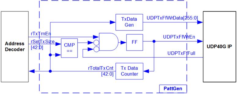
Figure 2‑10 PattGen block
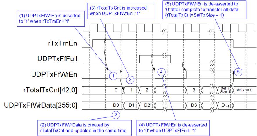
Figure 2‑11 PattGen Timing diagram
PattGen is designed to generate test data to UDP40G-IP. rTxTrnEn is asserted to ‘1’ when USER_CMD_REG[0] is set to ‘1’. When rTxTrnEn is ‘1’, UDPTxFfWrEn is controlled by UDPTxFfFull. UDPTxFfWrEn is de-asserted to ‘0’ when UDPTxFfFull is ‘1’. rTotalTxCnt is the data counter to check total data sent to UDP40G-IP. rTotalTxCnt is also used to generate 32-bit incremental data to UDPTxFfWrData signal. rTxTrnEn is de-asserted to ‘0’ when finishing transferring total data (total data is set by rSetTxSize).
Pattern Verification
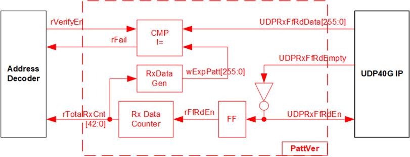
Figure 2‑12 PattVer block
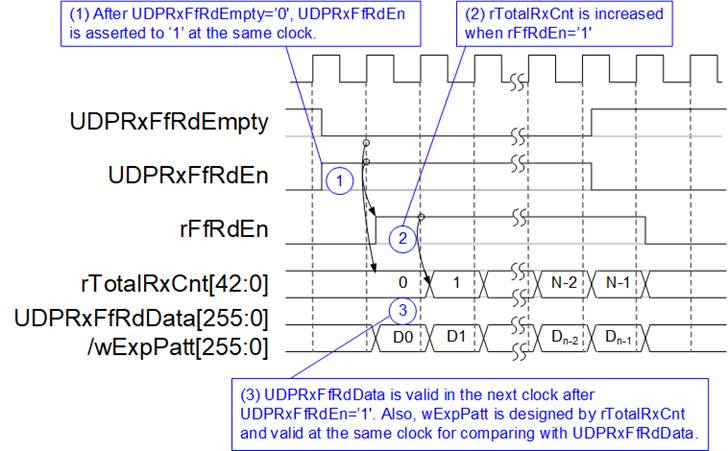
Figure 2‑13 PattVer Timing diagram
PattVer is designed to read test data from UDP40G-IP with or without data verification, depending on rVerifyEn flag. When rVerifyEn is set to ‘1’, data comparison is enabled to compare read data (UDPRxFfRdData) to the expected pattern (wExpPatt). When data verification is failed, rFail is asserted to ‘1’. UDPRxFfRdEn is designed by using NOT logic of UDPRxFfRdEmpty. UDPRxFfRdData is valid for data comparison in the next clock after asserting UDPRxFfRdEn to ‘1’. rRxFfRdEn which is one clock latency of UDPRxFfRdEn is applied to be counter enable of rTotalRxCnt to count total transfer size. rTotalRxCnt is used to generate wExpPatt.
3 CPU Firmware Sequence (FPGA)
After FPGA boot-up, 40G Ethernet link up status (USER_RST_REG[16]) is monitored. The CPU waits until link up is found. Next, welcome message is displayed and user selects the operation mode of UDP40G-IP to be client or server mode.
To initialize as client mode, UDP40G-IP sends ARP request to get the MAC address from the destination device. In server mode, UDP40G-IP waits until ARP request is received for decoding MAC address and returning ARP reply to finish initialization process.
When test environment uses two FPGA boards, the operation mode on two UDP40G-IPs must be different (one is client and another is server). To run with PC, it is recommended to set FPGA to as client mode. When PC receives ARP request, PC always returns ARP reply. It is not easy to force PC sending ARP request to FPGA.
The CPU firmware has two default parameters for each operation mode. Figure 3‑1 shows the example of the initialization sequence after system boot-up.
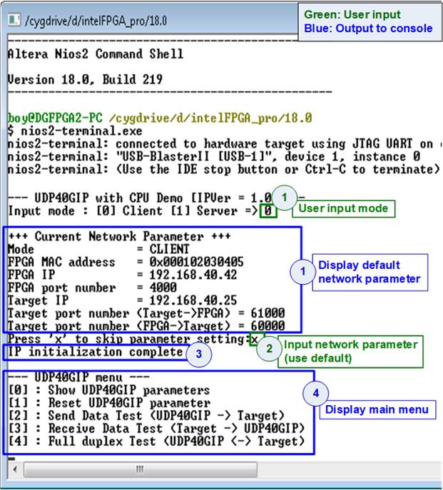
Figure 3‑1 Example of initialization sequence in client mode
There are four steps to complete initialization sequence as follows.
1) CPU receives the operation mode from user and displays default parameters on the console.
2) User inputs ‘x’ to complete initialization sequence by using default parameters. Other keys are set for changing some parameters. More details for changing some parameters are described in Reset IP menu (topic 3.2).
3) CPU waits until UDP40G-IP finishes initialization sequence (UDP40_CMD_REG[0]=’0’).
4) Main menu is displayed. There are five test operations for user selection. More details of each operation are described as follows.
3.1 Show parameters
This menu is used to show current parameters of UDP40G-IP, i.e. operation mode, FPGA MAC address, IP address, and port number. The step to display parameters is described as follows.
1) Read all network parameters from each variable in firmware.
2) Print out each variable.
3.2 Reset IP
This menu is used to change UDP40G-IP parameters such as IP address and source port number. After setting updated parameters to UDP40G-IP register, the CPU resets the IP to start re-initialization by using new parameters. Finally, the CPU monitors busy flag to wait until the initialization is completed. The step to reset IP is described as follows.
1) Display current parameter value to the console.
2) Receive initialization mode from user and confirm that input is valid. When the initialization mode is changed, the latest parameter set of the new mode is displayed on the console.
3) Receive remaining input parameters from user and check input value whether valid or not. When the input is invalid, the old value still be used.
4) Force reset to UDP40G-IP by setting UDP40_RST_REG[0]=’1’.
5) Set all parameters to UDP40G-IP register such as UDP40_SML/SMH_REG and UDP40_DIP_REG.
6) De-assert UDP40G-IP reset by setting UDP40_RST_REG[0]=’0’.
7) Reset UserReg by setting USER_RST_REG[0]=’1’.
8) Read UDP40G-IP busy flag (UDP40_CMD_REG[0]). Wait until busy flag is de-asserted to ‘0’ to confirm that initialization sequence is finished.
3.3 Send data test
User needs to input two parameters, i.e. total transmit length and packet size. The operation is cancelled when the input is invalid. 32-bit incremental pattern is generated from the logic and sent to the target (PC or FPGA). The received data is verified by the target (PC or FPGA). After all data are transferred completely, the operation is finished. More details of this menu are described as follows.
1) Receive transfer size and packet size from user and verify that all inputs are valid.
2) Set UserReg registers, i.e. transfer size (USER_TXLENL/H_REG), reset flag to clear start value of test pattern (USER_RST_REG[0]=’1’), and command register to start data pattern generator (USER_CMD_REG=0). After that, test pattern generator in UserReg generates test data to UDP40G-IP.
3) Display recommended parameter of test application running on PC from the current system parameters. Wait until user press any keys to start IP sending operation.
4) Set parameters to UDP40G-IP to start operation, i.e. Packet size to UDP40_PKL_REG and total size to UDP40_TDL/H_REG. After that, UDP40_CMD_REG is set to 1 to start IP sending data.
5) Wait until UDP40G-IP completes operation by monitoring IP busy flag (UDP40_CMD_REG[0] =’0’). During sending data, CPU reads current transfer size from user logic (USER_TXLENL/H_REG) and displays on the console every second.
6) When operation is finished, CPU calculates performance and displays test result on the console.
3.4 Receive data test
User needs to input two parameters, i.e. total received size and data verification mode (enable or disable). The operation is cancelled when the input is invalid. During the test, 32-bit incremental data is generated to verify the received data from PC/FPGA when data verification mode is enabled. The step of this test is described as follows.
1) Receive total transfer size and data verification mode from user and verify that all inputs are valid.
2) Set UserReg registers, i.e. reset flag to clear start value of test pattern (USER_RST_REG) and data verification mode (USER_CMD_REG[1]=’0’ or ‘1’).
3) Display recommended parameter of test application on PC (same as Step 3 of Send data test).
4) Wait until IP receives the first packet by monitoring current received size (USER_RXLENL/H_REG) that is not equal to ‘0’. After that, start timer.
5) Wait until received size (USER_RXLENL/H_REG) does not change more than 100 msec or total data are received. During waiting the data, CPU reads current received size from user logic (USER_RXLENL/H_REG) and displays on the console every second.
6) Stop timer. Check interrupt from timeout (USER_RST_REG[8]) and data verification flag (USER_CMD_REG[1]) register when verification mode is applied. When some errors are found, error message is displayed.
7) Calculate performance and display test result on the console.
3.5 Full duplex test
This menu is designed to run full duplex test by transferring data between FPGA and PC/FPGA in both directions by using different port number at the same time. Three inputs are received from user, i.e. total size for both directions, packet size for FPGA sending logic, and data verification mode for FPGA receiving logic.
To run full duplex test by using PC, user opens two “udpdatatest” applications on two consoles. First application is run to receive data with FPGA and another application is run to send data with FPGA. The port number using in two applications must be different. In case of two FPGAs test environment, only one port is applied to set to each FPGA. The step of this test is described as follows.
1) Receive total data size, packet size, and data verification mode from user and verify that all inputs are valid.
2) Set UserReg registers, i.e. transfer size (USER_TXLENL/H_REG), reset flag to clear start value of test pattern (USER_RST_REG), and command register to start data pattern generator with data verification mode (USER_CMD_REG=1 or 3).
3) Display the recommended parameter of test application running on PC from the current system parameters.
4) Set UDP40G-IP registers, i.e. packet size (UDP40_PKL_REG), total transfer size (UDP40_TDL/H_REG), and write command (UDP40_CMD_REG=1). After that, IP starts sending data operation. At the same time, IP is always ready to receive data without the additional setting.
5) Wait until the operation is finished for both sending and receiving direction.
a. In sending data, CPU waits until UDP40G-IP busy flag (UDP40_CMD_REG[0])=’0’.
b. In receiving data, CPU waits until total received size is equal to set value or total received size does not change for 100 msec (timeout condition).
During waiting the operation finishing, CPU reads current transfer size of both directions from user logic (USER_TXLENL/H_REG and USER_RXLENL/H_REG) and displays the result on the console every second.
6) Check interrupt from timeout (USER_RST_REG[8]) and data verification flag (USER_CMD_REG[1]) register when verification mode is applied. When some errors are found, error message is displayed.
7) Calculate performance and display test result on the console.
3.6 Function list in User application
This topic describes the function list to run UDP40G-IP operation.
|
void init_param(void) |
|
|
Parameters |
None |
|
Return value |
None |
|
Description |
Set network parameters to UDP40G-IP register from global parameters. After reset is de-asserted, it waits until UDP40G-IP busy flag is de-asserted to ‘0’. |
|
int input_param(void) |
|
|
Parameters |
None |
|
Return value |
0: Valid input, -1: Invalid input |
|
Description |
Receive network parameters from user, i.e. Mode, FPGA MAC address, FPGA IP address, FPGA port number, Target IP address, and Target port number for both transfer directions. When the input is valid, the parameters are updated. Otherwise, the value does not change. After receiving all parameters, the current value of each parameter is displayed. |
|
void show_cursize(void) |
|
|
Parameters |
None |
|
Return value |
None |
|
Description |
Read USER_TXLENL/H_REG and USER_RXLENL/H_REG, and then display the current transmitted and received size in Byte, KByte, or MByte unit |
|
void show_interrupt(void) |
|
|
Parameters |
None |
|
Return value |
None |
|
Description |
Read interrupt status from UDP40_TMO_REG and decode interrupt type to display the details of interrupt on the console. |
|
void show_param(void) |
|
|
Parameters |
None |
|
Return value |
None |
|
Description |
Display the current value of the network parameters set to UDP40G-IP such as IP address, MAC address, and port number. |
|
void show_result(void) |
|
|
Parameters |
None |
|
Return value |
None |
|
Description |
Read USER_TXLENL/H_REG and USER_RXLENL/H_REG to display total transmit size and total received size. Read the global parameters (timer_val and timer_upper_val) and calculate total time usage to display in usec, msec, or sec unit. Finally, transfer performance is calculated and displayed on MB/s unit. |
|
int udp40g_recv_test(void) |
|
|
Parameters |
None |
|
Return value |
0: The operation is successful -1: Receive invalid input or error is found |
|
Description |
Run Receive data test following description in topic 3.4. |
|
int udp40g_send_test(void) |
|
|
Parameters |
None |
|
Return value |
0: The operation is successful -1: Receive invalid input or error is found |
|
Description |
Run Send data test following description in topic 3.3. |
|
int udp40g_txrx_test(void) |
|
|
Parameters |
None |
|
Return value |
0: The operation is successful -1: Receive invalid input or error is found |
|
Description |
Run Full duplex test following described in topic 3.5. |
|
void wait_ethlink(void) |
|
|
Parameters |
None |
|
Return value |
None |
|
Description |
Read USER_RST_REG[16] and wait until ethernet is linked up |
4 Test Software (PC)
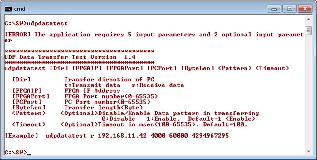
Figure 4‑1 udpdatatest application parameter
“udpdatatest” is an application on PC for sending or receiving UDP data. There are five parameters and two optional parameters. The parameter input should be matched to parameter set on FPGA. More details of each parameter input are as follows.
1) Dir : t – when PC sends data to FPGA
r – when PC receives data from FPGA
2) FPGAIP : IP address setting on FPGA (default value in FPGA is 192.168.40.42)
3) FPGAPort : Port number of FPGA (default value in FPGA is 4000)
4) PCPort : PC port number for sending or receiving data
(default is 60001 for PC to FPGA and 60000 for FPGA to PC)
5) ByteLen : Transfer length for sending or receiving in byte unit. This value must be
aligned to 32 from UDP40G-IP limitation.
6) Pattern (optional): Default value when user does not input this parameter is 1.
0 – Generate dummy data in transmit mode or disable data verification
in receive mode.
1 – Generate incremental data in transmit mode or enable data verification in receive mode.
7) Timeout (optional): Timeout for receiving data in msec unit.
Default value when user does not input this parameter is 100.
100 ms is recommended value for running with UDP40G-IP.
Receive data mode
The step when running the test application in receive mode is described as follows.
1) Get parameters from user and verify that the input is valid.
2) Create the socket and then set properties of received buffer.
3) Set IP address and port number from user parameter and then connect.
4) Repeat to read data until total data is equal to set value or no more data is received with timeout asserting. During reading data, the application prints total received data on the console every second.
a) When Pattern=1, the read data is verified by 32-bit incremental pattern which is increased every 4-byte received data.
b) When Pattern=0, the read data is not verified.
5) When the read loop is finished by timeout condition, “Timeout” message is displayed with total lost size and total received size.
6) After finishing the operation, the application displays performance as a test result.
Transmit data mode
The step when running the test application in transmit mode is described as follows.
1) Follow step (1)-(3) in Receive data mode.
2) Send data to the send buffer for sending out. During sending data, the application prints total sent data on the console every second.
a) When Pattern=1, the send buffer is filled by 32-bit incremental pattern.
b) When Pattern=0, the send buffer is not filled. Dummy data is applied in the test.
3) After finishing sending all data, the application displays performance with total data size as a test result.
5 Revision History
|
Revision |
Date |
Description |
|
1.0 |
22-Oct-19 |
Initial release |
Copyright: 2019 Design Gateway Co,Ltd.