AES256 IP Core Data Sheet

Core Facts |
|
|
Provided with Core |
|
|
Documentation |
User Guide, Design Guide |
|
Design File Formats |
Encrypted File |
|
Instantiation Templates |
VHDL |
|
Reference Designs & Application Notes |
Quartus Project, See Reference Design Manual |
|
Additional Items |
Demo on A10SoC, Agilex F-Series development kit |
|
Support |
|
|
Support Provided by Design Gateway Co., Ltd. |
|
Design Gateway Co.,Ltd
E-mail: ip-sales@design-gateway.com
URL: design-gateway.com
Features
· Support AES ECB mode standard.
· Support 256-bit key size.
· Support input data width128-bit.
· Throughput rate at 8.53 Mbits/MHz.
· Speed up to 3.41 Gbps @400MHz.
· 128-bit data calculation time is constant at 15 clock cycles.
Table 1: Example Implementation Statistics for Encryption
|
Family |
Example Device |
Fmax (MHz) |
ALMs |
Registers1 |
Design Tools |
|
Agilex F-Series |
AGFB014R24A2E2VR0 |
400 |
1349.7 |
649 |
Quartus 20.4 |
|
Arria10 SX |
10AS066N3F40E2SGE2 |
300 |
1265.2 |
386 |
Quartus 20.4 |
|
Stratix10 GX2 |
1SG280HU2F50E1VG |
325 |
1272.6 |
1447 |
Quartus 20.4 |
Table 2: Example Implementation Statistics for Decryption
|
Family |
Example Device |
Fmax (MHz) |
ALMs |
Registers1 |
Design Tools |
|
Agilex F-Series |
AGFB014R24A2E2VR0 |
400 |
1436.9 |
785 |
Quartus 20.4 |
|
Arria10 SX |
10AS066N3F40E2SGE2 |
300 |
1404.2 |
409 |
Quartus 20.4 |
|
Stratix10 GX2 |
1SG280HU2F50E1VG |
325 |
1394.5 |
2327 |
Quartus 20.4 |
Notes:
1) Actual logic resource is dependent on percentage of unrelated logic.
2) The results were obtained from implementation in the same environment, but have not been tested on the actual board.
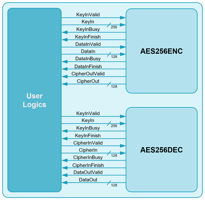
Figure 1: Block Diagram
General Description
AES256 IP Core (AES256IP) implement the advanced encryption standard (AES) algorithm which is widely used in many applications like file encryption, processor security, and secure file transfer protocol.
AES is a symmetric block cipher algorithm of the Rijndael family. Please find more details in the Federal Information Processing Standards Publication (FIPS PUB) 197.
AES256IP is consisted of AES256ENC module, that is encryption module and AES256DEC module, that is decryption module as shown in Figure 1.
Functional Description
1. AES256ENC
Table 3: Interface signals of AES256ENC
|
Signal name |
Dir |
Description |
|
RstB |
In |
IP core system reset. Active low. |
|
Clk |
In |
IP core system clock. |
|
Key setting signals |
||
|
KeyInValid |
In |
KeyInValid is a user signal to specify data valid of KeyIn. Assert to ‘1’ to indicate that KeyIn is valid and start key setting.
|
|
KeyIn[255:0] |
In |
KeyIn is 256-bit key data of key setting. KeyIn must be valid when KeyInValid is asserted to ‘1’.
|
|
KeyInBusy |
Out |
KeyInBusy specifies busy status of Key setting. Assert to ‘1’ after user set KeyInValid, until the last cycle of operation. KeyInValid or DataInValid will be ignored while KeyInBusy is ‘1’.
|
|
KeyInFinish |
Out |
KeyInFinish specifies finish status of Key setting. Assert to ‘1’ at the last cycle of operation.
|
|
Encryption control signals |
||
|
DataInValid |
In |
DataInValid is a user signal to specify data valid of DataIn. Assert to ‘1’ to indicate that DataIn is valid and start encryption process.
|
|
DataIn[127:0] |
In |
DataIn is 128-bit input data. DataIn must be valid when DataInValid is asserted to ‘1’.
|
|
DataInBusy |
Out |
DataInBusy specifies busy status of encryption. Assert to ‘1’ after user set DataInValid, until the last cycle of operation. KeyInValid or DataInValid will be ignored while DataInBusy is ‘1’.
|
|
DataInFinish |
Out |
DataInFinish specifies finish status of encryption. Assert to ‘1’ at the last cycle of operation. |
|
CipherOutValid |
Out |
CipherOutValid specify data valid for CipherOut. Assert to ‘1’ when encryption finished.
|
|
CipherOut[127:0] |
Out |
CipherOut is 128-bit data output of encryption. Valid when CipherOutValid is asserted to ‘1’.
|
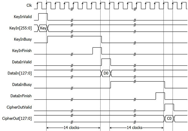
Figure 2: AES256ENC operation timing diagram
AES256ENC operation is as simple as 2 steps to use as below.
1.1. Key setting
Key setting is the first step to use AES256ENC. As shown in Figure 2, AES256ENC is started key setting process when KeyInValid=‘1’ and takes 14 clock cycles to finish the process (KeyInBusy=‘0’). After that, this KeyIn is used for every encryption and can be changed via KeyInValid is asserted to ‘1’.
1.2. Encryption control
As shown in Figure 2. After key setting, AES256ENC starts the process when DataInValid=‘1’. DataInBusy is set to be ‘1’ in next cycle and wait for 14 clock cycles, Process will finish when DataInBusy is set to be ‘0’. After that, Encrypted data is set to CipherOut[127:0] signal while CipherOutValid signal is set to be ‘1’.
For the best performance of encryption process, Figure 3 shows the timing diagram of continuous and pipelining encryption. User can used DataInFinish signal to generate DataInValid in the next cycle for start next encrytion.
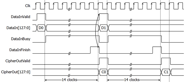
Figure 3: Continuous and pipelining encryption
2. AES256DEC
Table 4: Interface signals of AES256DEC
|
Signal name |
Dir |
Description |
|
RstB |
In |
IP core system reset. Active low. |
|
Clk |
In |
IP core system clock. |
|
Key setting signals |
||
|
KeyInValid |
In |
KeyInValid is a user signal to specify data valid of KeyIn. Assert to ‘1’ to indicate that KeyIn is valid and start key setting.
|
|
KeyIn[255:0] |
In |
KeyIn is 256-bit key data of key setting. KeyIn must be valid when KeyInValid is asserted to ‘1’.
|
|
KeyInBusy |
Out |
KeyInBusy specifies busy status of Key setting. Assert to ‘1’ after user set KeyInValid, until the last cycle of operation. KeyInValid or CipherInValid will be ignored while KeyInBusy is ‘1’.
|
|
KeyInFinish |
Out |
KeyInFinish specifies finish status of Key setting. Assert to ‘1’ at the last cycle of operation.
|
|
Decryption control signals |
||
|
CipherInValid |
In |
CipherInValid is a user signal to specify data valid of CipherIn. Assert to ‘1’ to indicate that CipherIn is valid and start decryption process.
|
|
CipherIn[127:0] |
In |
CipherIn is 128-bit encrypted input data. CipherIn must be valid when CipherInValid is asserted to ‘1’.
|
|
CipherInBusy |
Out |
CipherInBusy specifies busy status of decryption. Assert to ‘1’ after user set CipherInValid, until the last cycle of operation. KeyInValid or CipherInValid will be ignored while CipherInBusy is ‘1’.
|
|
CipherInFinish |
Out |
CipherInFinish specifies finish status of decryption. Assert to ‘1’ at the last cycle of operation.
|
|
DataOutValid |
Out |
DataOutValid specify data valid for DataOut. Assert to ‘1’ when decryption finished.
|
|
DataOut[127:0] |
Out |
DataOut is 128-bit data output of decryption. Valid when DataOutValid is asserted to ‘1’.
|
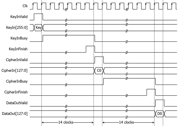
Figure 4: AES256DEC operation timing diagram
AES256DEC operation is as simple as 2 steps to use as below.
2.1. Key setting
Key setting is the first step to use AES256DEC. As shown in Figure 4, AES256DEC is started key setting process when KeyInValid=‘1’ and takes 14 clock cycles to finish the process (KeyInBusy=‘0’). After that, this KeyIn is used for every decryption and can be changed via KeyInValid is asserted to ‘1’.
2.2. Decryption control
As shown in Figure 4. After key setting, AES256DEC starts the process when CipherInValid=‘1’. CipherInBusy is set to be ‘1’ in next cycle and wait for 14 clock cycles, Process will finish when CipherInBusy is set to be ‘0’. After that, decrypted data is set to DataOut[127:0] signal while DataOutValid signal is set to be ‘1’.
For the best performance of decryption process, Figure 5 shows timing diagram of continuous and pipelining decryption. User can used CipherInFinish signal to generate CipherInValid in the next cycle for start next decryption.
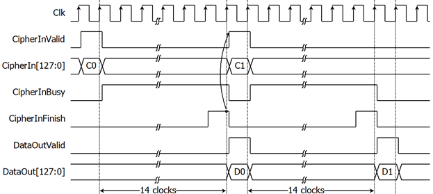
Figure 5: Continuous and pipelining decryption
Verification Methods
AES256 IP Core functionality were verified on real board design by using Agilex F-Series development kit and Arria10 SoC development board.
Recommended Design Experience
The user must be familiar with HDL design methodology to integrate this IP into system.
Ordering Information
This product is available directly from Design Gateway Co., Ltd. Please contact Design Gateway Co., Ltd. For pricing and additional information about this product using the contact information on the front page of this datasheet.
Revision History
|
Revision |
Date |
Description |
|
1.00 |
10/Sep/2021 |
New release |
|
1.02 |
26/Oct/2022 |
New design to improve performance |
|
1.03 |
15/Feb/2023 |
Add more resource information |