This document describes the instruction to demonstrate the operation of AES256IP on FPGA development boards. In the demonstration, AES256IP are used to encrypt and decrypt data between two memories in FPGA. User can fill memory with plain or cipher data patterns, set encryption/decryption key and control test operation via Nios II Command Shell.
1 Environment Setup
To operate AES256IP demo, please prepare following test environment.
1) FPGA development board
Agilex F-series development kit
Arria10 SoC Development board
2) Test PC.
3) Micro USB cable for JTAG connection connecting between FPGA boards and Test PC.
4) Quartus programmer for programming FPGA and Nios II command shell, installed on PC.
5) SOF file named “AES256.sof” (To download these files, please visit our web site at www.design-gateway.com)
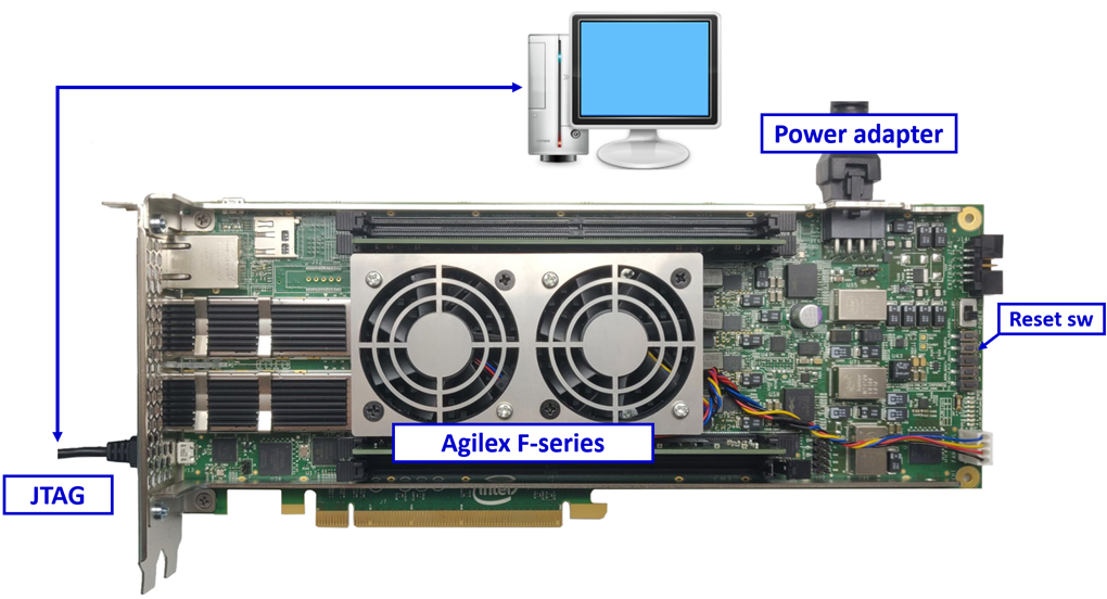
Figure 1‑1 AES256IP demo environment on Agilex F-series board
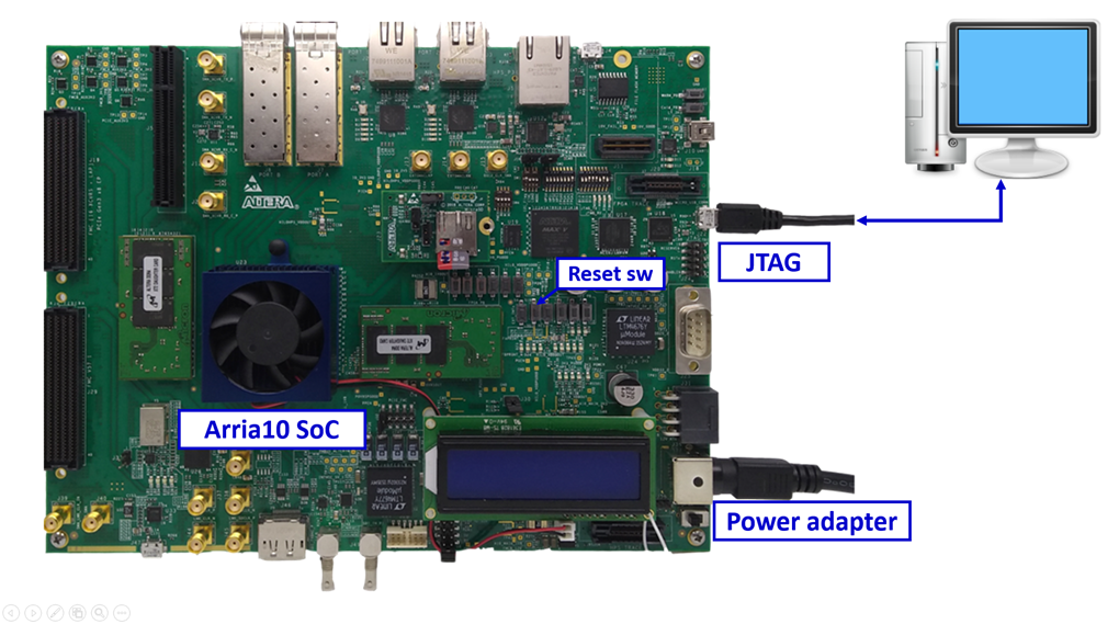
Figure 1‑2 AES256IP demo environment on Arria10 SoC board
2 FPGA development board setup
1) Make sure power switch is off and connect power supply to FPGA development board.
2) Connect USB cables between FPGA board and PC via micro-USB ports.
3) Turn on power switch for FPGA board.
4) Open Quartus Programmer to program FPGA through USB-1 by following step.
i) Click “Hardware Setup…” to select
AGF FPGA Development Kit [USB-1] for Agilex F-series
USB-BlasterII [USB-1] for Arria10 SoC
ii) Click “Auto Detect” and select FPGA number.
iii) Select FPGA device icon (Agilex or A10SoC).
iv) Click “Change File” button, select SOF file in pop-up window and click “open” button.
v) Check “program”.
vi) Click “Start” button to program FPGA.
vii) Wait until Progress status is equal to 100%.
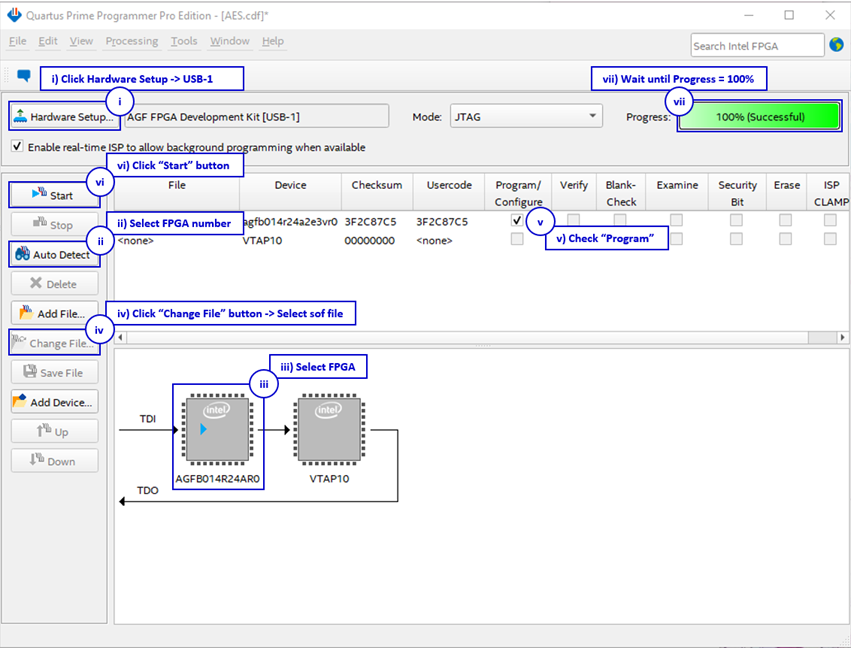
Figure 2‑1 FPGA Programmer for Agilex
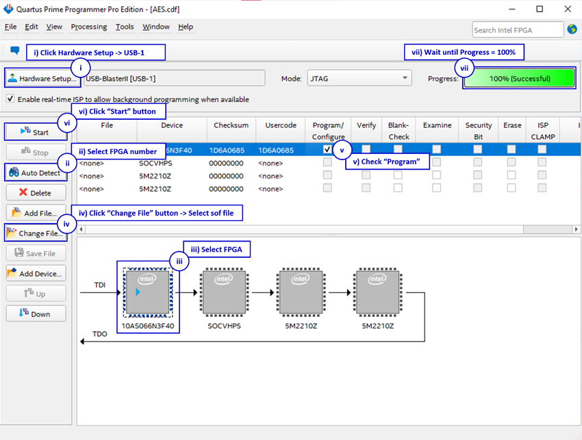
Figure 2‑2 FPGA Programmer for A10SoC
For A10SoC after program SOF file complete, Quartus Prime will show popup message of Intel FPGA IP Evaluation Mode Status as shown in Figure 2‑3. Please do not press cancel button.
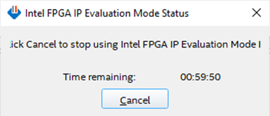
Figure 2‑3 Intel FPGA IP Evaluation Mode Status
3 Nios II Command Shell
User can fill RAMs with plain or cipher data patterns, set encryption/decryption key and control test operation via Nios II Command Shell. When configuration is completed, AES256demo command menu will be displayed as shown in Figure 3‑1. The detailed information of each menu is described in topic 4.
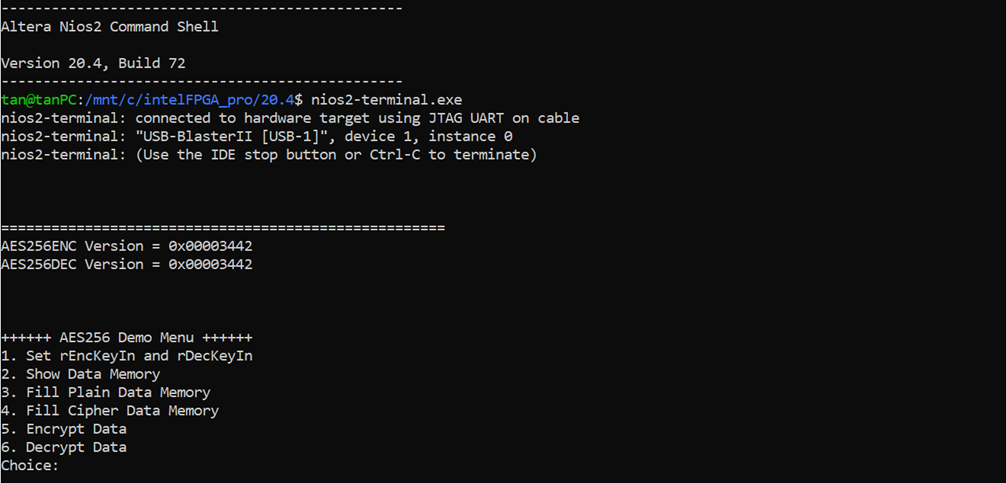
Figure 3‑1 Nios II Command Shell
4 Command detail and testing result
4.1 Set encryption/decryption key
Step to set encryption key and decryption key as follows
a) Select “1. Set rEncKeyIn and rDecKeyIn”.
b) Current encryption key will be displayed on Nios II Command Shell as shown in Figure 4‑1.
c) Set new encryption key: User is allowed to input new key in hex format or press “enter” to skip setting new key. Then the current encryption key is printed again.
d) Current decryption key will be displayed on Nios II Command Shell.
e) Set new decryption key: User is allowed to input new key in hex format or press “enter” to use rEncKeyIn as rDecKeyIn. Then the current decryption key is printed again.
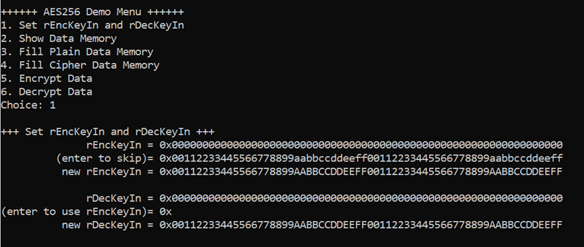
Figure 4‑1 Set rEncKeyIn and rDecKeyIn example
4.2 Show Data Memory
To show data in memory, user can select “2. Show Data Memory” and input the desired number of 128-bit data to show. Both plain data and cipher data will be displayed in table-form as shown in Figure 4‑2. User can press “enter” key to skip putting the number of data, then Nios II Command Shell will display five rows (default value) of 128-bit plain data and 128-bit cipher data at address 0x0000-0x004F.
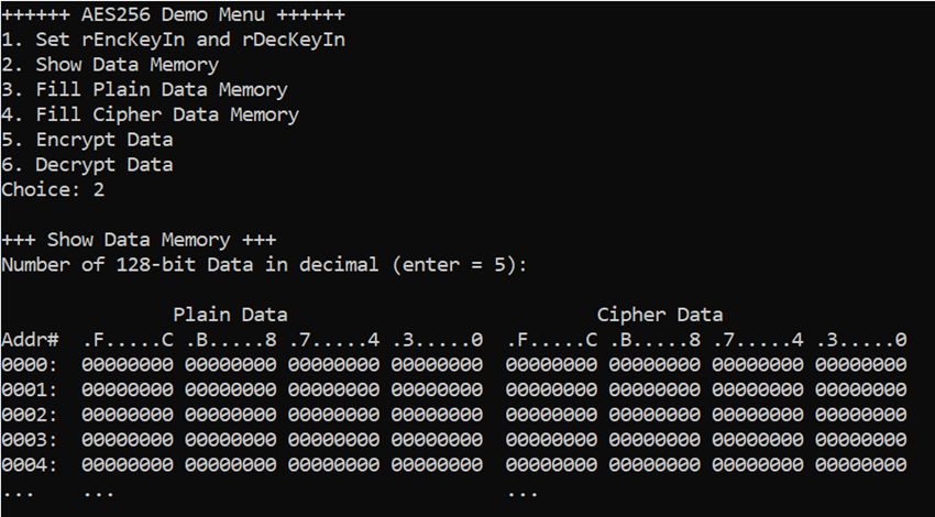
Figure 4‑2 Displayed Data when press “enter” key
4.3 Fill Plain Data Memory
Step to fill plain data in memory as follows
a) Select “3. Fill Plain Data Memory”.
b) There are four pattern to fill memory.
a. zero pattern
b. 8-bit counter
c. 16-bit counter
d. 32-bit counter
c) Whole plain-data memory is filled with selected data pattern.
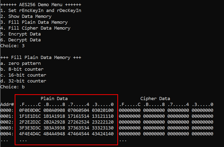
Figure 4‑3 Displayed Data when select pattern b
4.4 Fill Cipher Data Memory
Step to fill Cipher data in memory as follows
a) Select “4. Fill Cipher Data Memory”.
b) There are four pattern to fill memory.
a. zero pattern
b. 8-bit counter
c. 16-bit counter
d. 32-bit counter
c) Whole cipher-data memory is filled with selected data pattern.
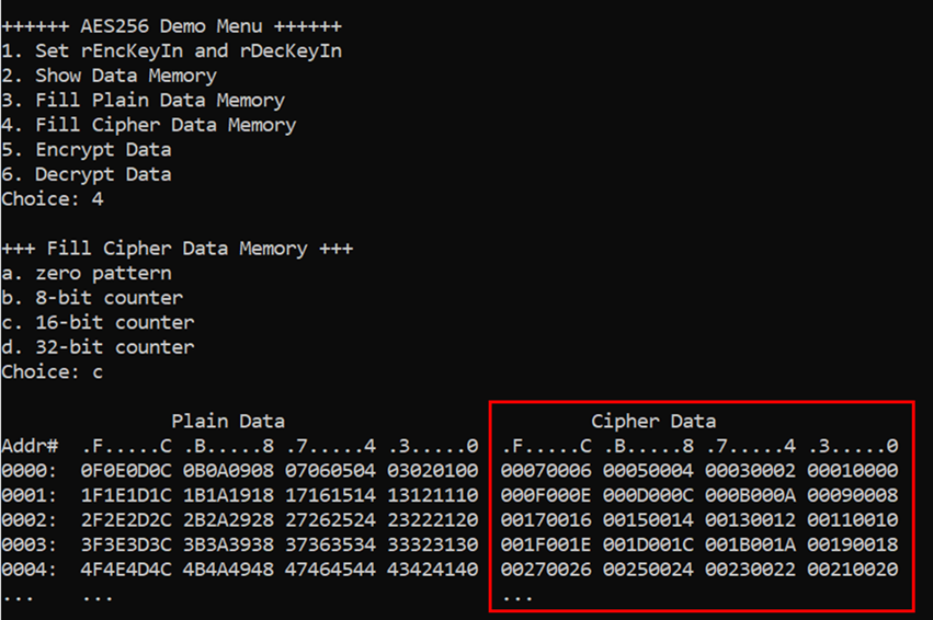
Figure 4‑4 Displayed Data when select pattern c
4.5 Encrypt
Select “5. Encrypt” to encrypt plain data in memory. User can input the desired number of plain data to encrypt or press “enter” key to encrypt five 128-bit plain data. When the encryption process is finished, DpRam2 will be filled with cipher data from AES256ENC.
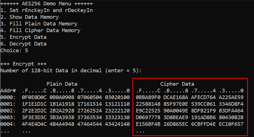
Figure 4‑5 Nios II Command Shell after finished encryption process
4.6 Decrypt
Select “6. Decrypt” to decrypt cipher data in memory. User can input the desired number of cipher data to decrypt or press “enter” key to decrypt five 128-bit Cipher data. When the decryption process is finished, DpRam1 will be filled with plain data from AES256DEC.
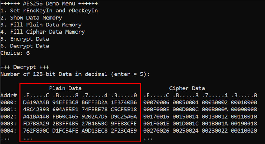
Figure 4‑6 Nios II Command Shell after finished decryption process
5 Revision History
|
Revision |
Date |
Description |
|
1.00 |
10-Sep-2021 |
Initial version release |
|
1.02 |
27-Oct-2022 |
Update description for new design |
|
1.03 |
15-Nov-2022 |
Correct reference figure number. |