Rev1.02 29-Aug-2023
3.1 Set encryption/decryption key
1 Introduction
This document describes the detail of AES256SSIP reference design. In this reference design, AES256SSIP are used to encrypt and decrypt data between two memories in FPGA. User can fill memory with plain or cipher data patterns, set encryption/decryption key and control test operation via serial console on test PC. More details of the hardware design and CPU firmware are described as follows.
2 Hardware Overview
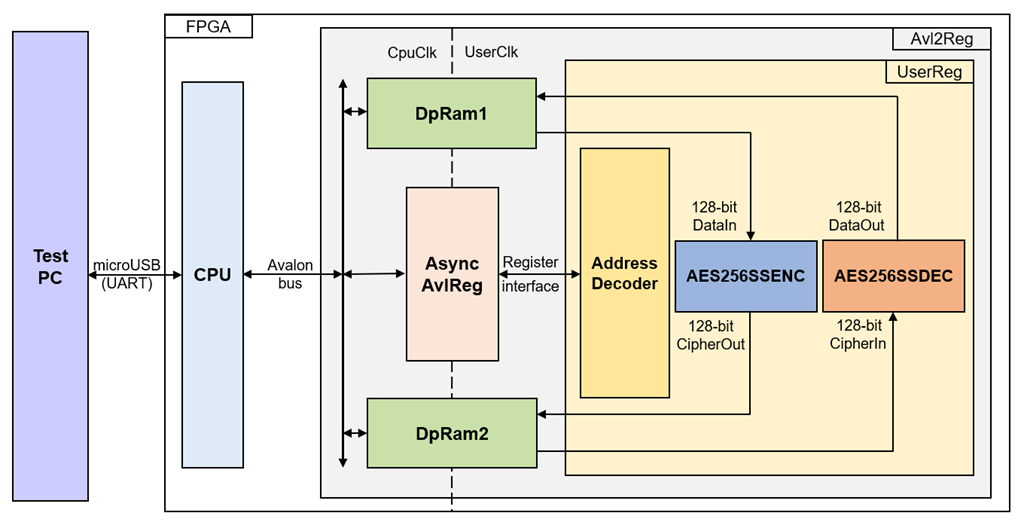
Figure 2‑1 AES256SSIP reference design block diagram
In this test environment, AES256SSENC and AES256SSDEC interface with two dual-port RAMs with asymmetric ports, which are DpRam1 and DpRam2, as shown in Figure 2‑1. AES256SSIP is sub-modules in UserReg module within Avl2Reg. CPU system is designed to interface with FPGA logic through Avalon-MM bus and interface with user through serial console in test PC.
For user control interface, there are registers in UserReg to store parameters from user such as encryption/decryption key, number of data to encrypt or decrypt. Input parameters are received from user via serial console.
For user data interface, UserReg is designed to be able to write pattern data or read data in RAMs following user’s command. DpRam1 is used to store the plain data from user which will be input data for AES256SSENC in encryption mode or the decrypted data which is output data from AES256SSDEC in decryption mode. DpRam2 is used to store the cipher data from user which will be input data for AES256SSDEC in decryption mode or encrypted data which is output data from AES256SSENC in encryption mode.
Because CPU system and AES256SSENC/AES256SSDEC run in different clock domain, AsyncAvlReg module inside Avl2Reg is designed as asynchronous circuit to support clock-crossing operation. Also, AsyncAvlReg converts Avalon-MM bus signal which is standard bus in CPU system to be register interface. The details of Avl2Reg module are described as follows.
2.1 Avl2Reg
Avl2Reg module is connected to CPU through Avalon-MM bus. The hardware registers are mapped to CPU memory address, as shown in Table 2-1. The control and status registers for CPU access are designed in Avl2Reg.
Avl2Reg consists of AsyncAvlReg, DpRam and UserReg. Avl2Reg selects the path for Avalon-MM signals during transmission to AsyncAvlReg or stored in DpRam. When CPU access to hardware, SAvlAddress [13:9] are used to decode that CPU accesses dual-port ram (DpRam) or AsyncAvlReg. If CPU accesses DpRam (SAvlAddress [13:9]=“00001” or “00010”), DpRam will be write or read data at Address SAvlAddress[8:0]. Otherwise, Avl2Reg will be transmission to AsyncAvlReg. Additionally, as shown in Figure 2-1, there are two clock domains applied in this block, i.e., CpuClk which is used to interface with CPU through Avalon-MM bus and UserClk which is user clock domain for AES256SSENC/AES256SSDEC. AsyncAvlReg includes asynchronous circuit between CpuClk and UserClk.
UserReg includes the register file of the parameters and the status signals of test logics, including AES256SSIP. Both data interface and control interface of AES256SSIP are connected to UserReg. More details of AsyncAvlReg and UserReg are described as follows.
2.2 AsyncAvlReg
AsyncAvlReg is designed to convert the Avalon-MM signals to be the simple register interface which has 32-bit data bus size (similar to Avalon-MM data bus size). Also, it enables two clock domains, CpuClk and UserClk domain, to communicate.
To write register, RegWrEn is asserted to ‘1’ with the valid signal of RegAddr (Register address in 32-bit unit), RegWrData (write data of the register), and RegWrByteEn (the byte enable of this access: bit[0] is write enable for RegWrData[7:0], bit[1] is used for RegWrData[15:8], …, and bit[3] is used for RegWrData[31:24]).
To read register, AsyncAvlReg asserts RegRdReq=’1’ with the valid value of RegAddr (the register address in 32-bit unit). After that, the module waits until RegRdValid is asserted to ‘1’ to get the read data through RegRdData signal at the same clock.
2.3 UserReg
This module is designed to write/read data in RAMs, control and check status of AES256SSENC/AES256SSDEC corresponding with write register access or read register request from AsyncAvlReg module. Memory map of data, control and status signals inside UserReg module is shown in Table 2-1. Timing diagram of register interface is shown in Figure 2-2.
Table 2-1 Register map Definition
|
Address offset |
Register Name |
Rd/Wr |
Description |
|
0x0000 |
ADDR_A1_REG |
Rd/Wr |
[6:0] – address A of DpRam1 (rAddrA1[6:0]). |
|
0x0004 |
ADDR_A2_REG |
Rd/Wr |
[6:0] – address A of DpRam2 (rAddrA2[6:0]). |
|
0x0008 |
ENC_CNT_REG |
Rd |
[8] – AES256SSENC KeyIn busy flag (wEncKeyInBusy). [7] – AES256SSENC DataIn busy flag (wEncDataInBusy). [6:0] – Current remaining data to encrypt (rEncCnt[6:0]). |
|
Wr |
[6:0] – Number of data to encrypt (rEncCnt[6:0]). |
||
|
0x000C |
DEC_CNT_REG |
Rd |
[8] – AES256SSENC KeyIn busy flag (wDecKeyInBusy). [7] – AES256SSDEC CipherIn busy flag (wDecCipherInBusy). [6:0] – Current remaining data to decrypt (rDecCnt[6:0]). |
|
Wr |
[6:0] – Number of data to decrypt(rDecCnt[6:0]). |
||
|
0x0018 |
ENC_VER_REG |
Rd |
[31:0] – AES256SSENC IP version (wEncVersion). |
|
0x001C |
DEC_VER_REG |
Rd |
[31:0] – AES256SSDEC IP version (wDecVersion). |
|
ENC_KEYIN_0_REG |
Rd/Wr |
[31:0] – Encryption key (rEncKeyIn[31:0]). |
|
|
0x0024 |
ENC_KEYIN_1_REG |
Rd/Wr |
[31:0] – Encryption key (rEncKeyIn[63:32]). |
|
0x0028 |
ENC_KEYIN_2_REG |
Rd/Wr |
[31:0] – Encryption key (rEncKeyIn[95:64]). |
|
0x002C |
ENC_KEYIN_3_REG |
Rd/Wr |
[31:0] – Encryption key (rEncKeyIn[127:96]). |
|
0x0030 |
ENC_KEYIN_4_REG |
Rd/Wr |
[31:0] – Encryption key (rEncKeyIn[159:128]). |
|
0x0034 |
ENC_KEYIN_5_REG |
Rd/Wr |
[31:0] – Encryption key (rEncKeyIn[191:160]). |
|
0x0038 |
ENC_KEYIN_6_REG |
Rd/Wr |
[31:0] – Encryption key (rEncKeyIn[223:192]). |
|
0x003C |
ENC_KEYIN_7_REG |
Rd/Wr |
[31:0] – Encryption key (rEncKeyIn[255:224]). |
|
0x0040 |
DEC_KEYIN_0_REG |
Rd/Wr |
[31:0] – Decryption key (rDecKeyIn[31:0]). |
|
0x0044 |
DEC_KEYIN_1_REG |
Rd/Wr |
[31:0] – Decryption key (rDecKeyIn[63:32]). |
|
0x0048 |
DEC_KEYIN_2_REG |
Rd/Wr |
[31:0] – Decryption key (rDecKeyIn[95:64]). |
|
0x004C |
DEC_KEYIN_3_REG |
Rd/Wr |
[31:0] – Decryption key (rDecKeyIn[127:96]). |
|
0x0050 |
DEC_KEYIN_4_REG |
Rd/Wr |
[31:0] – Decryption key (rDecKeyIn[159:128]). |
|
0x0054 |
DEC_KEYIN_5_REG |
Rd/Wr |
[31:0] – Decryption key (rDecKeyIn[191:160]). |
|
0x0058 |
DEC_KEYIN_6_REG |
Rd/Wr |
[31:0] – Decryption key (rDecKeyIn[223:192]). |
|
0x005C |
DEC_KEYIN_7_REG |
Rd/Wr |
[31:0] – Decryption key (rDecKeyIn[255:224]). |
|
0x0800~0x0FFF |
PLAIN_BASE_ADDR |
Rd/Wr |
[31:0] – Plain data in DpRam1 (wRdDataB1). |
|
0x1000~0x17FF |
CIPHER_BASE_ADDR |
Rd/Wr |
[31:0] – Cipher data in DpRam2 (wRdDataB2). |
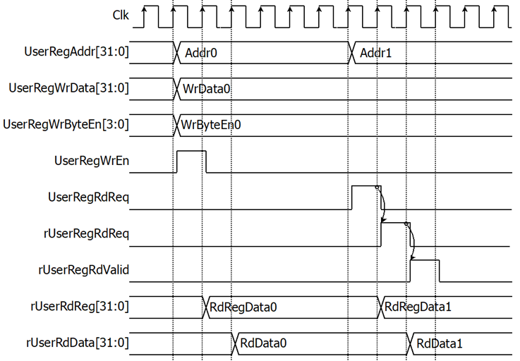
Figure 2‑2 Register interface timing diagram
To write register, UserRegWrEn is asserted to ‘1’ with the valid of UserRegAddr. UserRegAddr[15:11] are used to decode that CPU accesses dual-port ram (DpRam) or internal register area. If CPU accesses or internal register area (UserRegAddr[15:11]=“00000”), UserRegWrData is loaded to internal register which has matched UserRegAddr[10:0]. For example, rAddrA1 is loaded by UserRegWrData when UserRegAddr=0x0000.
To read register, one multiplexer is designed to select the read data within each address area. UserRegAddr[10:2] is applied in each Register area to select the data. Next, the address decoder uses UserRegAddr[15:11] to select the read data from each area for returning to CPU. As shown in Figure 2-2, read data is valid in next two clock cycles. When UserRegRdReq is active, rUserRegRdReq is asserted to ‘1’. Then rUserRdValid is active with the valid read value of UserRegAddr.
In this reference design, there are three main operations which are key setting, encryption and decryption. Each operation is described as follows.
2.3.1 Key setting
For encryption key setting, rEncKeyIn is set by writing register UserRegAddr=0x0020-0x003F as shown in Table 2-1. When ENC_KEYIN_0_REG is written (UserRegAddr=0x0020), rEncKeyIn[31:0] is set. Then rEncKeyInValid is asserted to ‘1’ as shown in Figure 2-3. The encryption key setting takes 14 clocks cycles to finish.
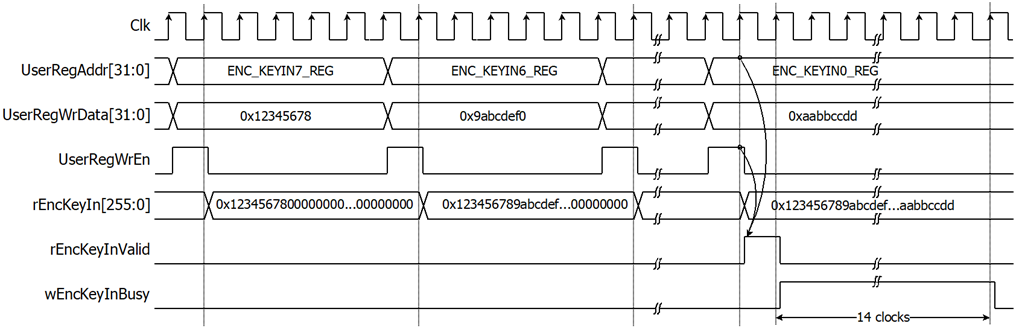
Figure 2‑3 Timing diagram of encryption key setting process
For decryption key setting, rDecKeyIn is set by writing register UserRegAddr=0x0040-0x005F as shown in Table 2-1. When DEC_KEYIN_0_REG is written (UserRegAddr=0x0040), rDecKeyIn[31:0] is set. Then rDecKeyInValid is asserted to ‘1’ and decryption key setting process is started as shown in Figure 2-4. The decryption key setting takes 14 clocks cycles to finish.
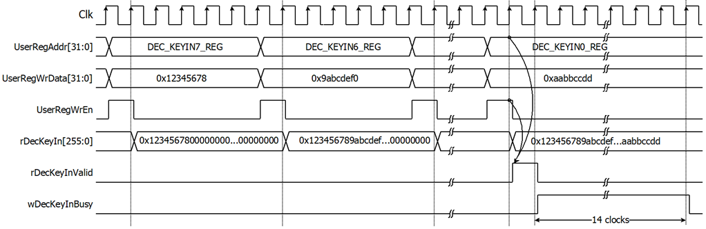
Figure 2‑4 Timing diagram of decryption key setting process
2.3.2 Encryption
For encryption process, 128-bit plain data, which will be input data for AES256SSENC, are stored in DpRam1. Before starting encryption process, address A of DpRam1 (rAddrA1) is set to 0x00 to access the first plain data. As shown in Figure 2-5, when UserRegAddr=0x0008 (ENC_CNT_REG) is written, UserRegWrData is loaded to rEncCnt as the number of data to encrypt, and rRamRdA1 is asserted to ‘1’ when rEncCnt>0. Then rAddrA1 is increased by 1 to access next plain data in. rEncDataInValid is delayed two clock cycle from rRamRdA1. When rEncCnt=0, no remaining data to encrypt and rRamRdA1 is cleared to ‘0’ in the next cycle.
Cipher data from AES256SSENC is stored in DpRam2. Before starting encryption process, address A of DpRam2 (rAddrA2) is set to 0x00 for writing the first output cipher data. When wEncCipherOut is active, wEncCipherOut is loaded to DpRam2. Then rAddrA2 is increased by 1 prepared for next cipher output.
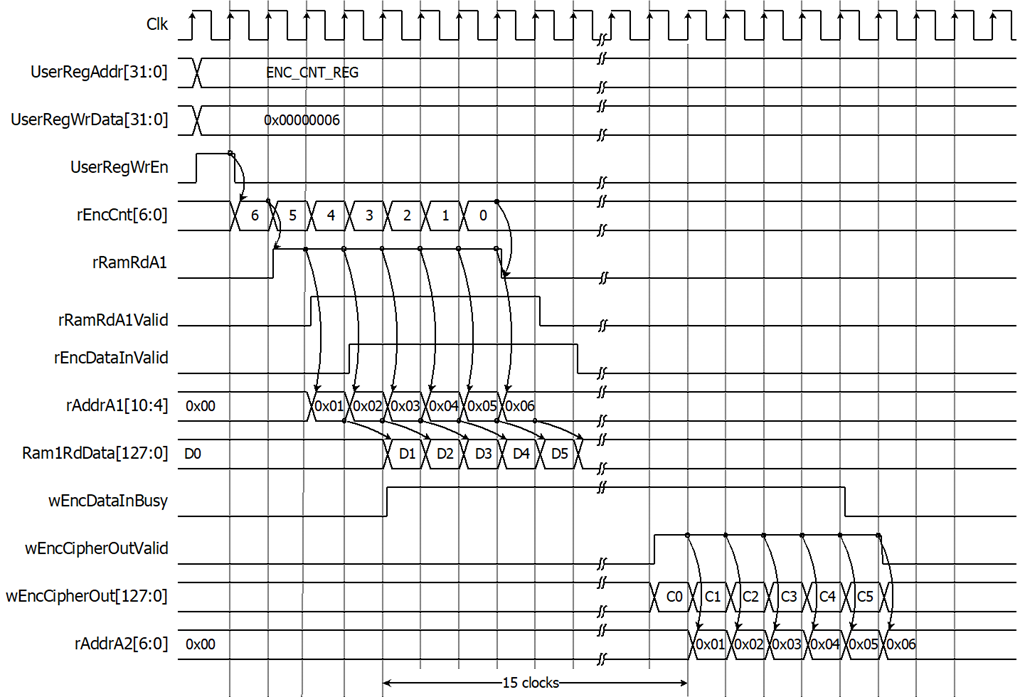
Figure 2‑5 Timing diagram of encryption process
Note: DpRam1/DpRam2 are designed for 2 clock latency of read.
2.3.3 Decryption
For decryption process, 128-bit cipher data, which will be input data for AES256SSDEC, are stored in DpRam2. Before starting decryption process, address A of DpRam2 (rAddrA2) is set to 0x00 to access the first cipher data. As shown in Figure 2-6, when UserRegAddr=0x000C (DEC_CNT_REG) is written, UserRegWrData is loaded to rDecCnt as the number of data to decrypt, and rRamRdA2 is asserted to ‘1’ when rDecCnt>0. Then rAddrA2 is increased by 1 to access next cipher data in. rDecCipherInValid is delayed two clock cycle from rRamRdA2. When rDecCnt=0, no remaining data to decrypt and rRamRdA2 is cleared to ‘0’ in the next cycle.
Decrypted data from AES256SSDEC is stored in DpRam1. Before starting decryption process, address A of DpRam1 (rAddrA1) is set to 0x00 for writing the first output plain data. When wDecDataOut is active, wDecDataOut is loaded to DpRam1. Then rAddrA1 is increased by 1 prepared for next plain output.
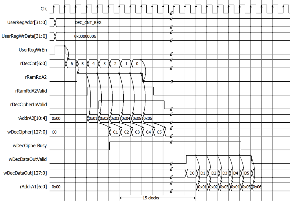
Figure 2‑6 Timing diagram of decryption process
3 CPU Firmware
After system boot up, CPU initializes its peripherals such as UART and Timer and shows IP version of AES256SSENC and AES256SSDEC. Then main menu is displayed. Main function runs in an infinite loop to show the main menu and get keyboard input from user. User can select each menu via serial console that will call the related functions. After functions finished running, the main menu is displayed again. More details of the sequence in each menu are described as follows.
3.1 Set encryption/decryption key
This menu is used to set encryption/decryption key. The sequence of the firmware is as follows.
1) Call change_key_set function to change encryption/decryption key set. User can input “enter” key to skip input encryption key and not change current enc_key_set or to skip input decryption key and change dec_key_set similar to enc_key_set.
2) Call set_enc_key function and set_dec_key function inside change_key_set function to set enc_key_set and dec_key_set to mapped registers.
change_key_set function, set_enc_key function and set_dec_key function is described in Table 3-1, Table 3-2 and Table 3-3, respectively.
Table 3-1 change_key_set function
|
void change_key_set(unsigned int *enc_key_set, unsigned int *dec_key_set) |
|
|
Parameter |
enc_key_set: pointer of array storing 256-bit encryption key dec_key_set: pointer of array storing 256-bit decryption key |
|
Return value |
None |
|
Description |
This function displays current encryption key on the console. Receive input new encryption key in hexadecimal format or “enter” key to skip. User’s input will be ignored if it is not hexadecimal format. The encryption/decryption key is stored in enc_key_set/dec_key_set. Then set_enc_key function and set_dec_key function is called, respectively. |
Table 3-2 set_enc_key set function
|
void set_enc_key(unsigned int *enc_key_set) |
|
|
Parameter |
enc_key_set: pointer of array storing 256-bit encryption key |
|
Return value |
None |
|
Description |
This function sets 256-bit encryption key to mapped registers which are ENC_KEYIN_7_REG, ENC_KEYIN_6_REG, ENC_KEYIN_5_REG, ENC_KEYIN_4_REG, ENC_KEYIN_3_REG, ENC_KEYIN_2_REG, ENC_KEYIN_1_REG and ENC_KEYIN_0_REG.When ENC_KEYIN_0_REG is set, rEncKeyInValid is asserted to ‘1’. Monitor AES256SSENC status until the key setting is completed. (*ENC_CNT_REG=0) |
Table 3-3 set_dec_key set function
|
void set_dec_key(unsigned int *dec_key_set) |
|
|
Parameter |
dec_key_set: pointer of array storing 256-bit decryption key |
|
Return value |
None |
|
Description |
This function sets 256-bit decryption key to mapped registers which are DEC_KEYIN_7_REG, DEC_KEYIN_6_REG, DEC_KEYIN_5_REG, DEC_KEYIN_4_REG, DEC_KEYIN_3_REG, DEC_KEYIN_2_REG, DEC_KEYIN_1_REG and DEC_KEYIN_0_REG. When DEC_KEYIN_0_REG is set, rDecKeyInValid is asserted to ‘1’. Monitor AES256SSDEC status until the key setting is completed. (*DEC_CNT_REG=0) |
3.2 Show Data Memory
This menu is used to show data in memory. User can set the number of 128-bit data to show on console. The sequence of the firmware is as follows.
1) Receive the number of 128-bit data in decimal format or “enter” key to use default value. If user input ‘0’, the number of 128-bit data to show will be default value. The number of 128-bit data to show is stored in length128.
2) Call show_data function to show data in memory with length128 as its parameter. show_data function is described in Table 3-4.
Table 3-4 show_data function
|
void show_data(unsigned int length128) |
|
|
Parameter |
length128: number of 128-bit data to show |
|
Return value |
None |
|
Description |
This function shows data in both DpRam1 and DpRam2 corresponding to length. CPU firmware reads data in DpRam1, starting at PLAIN_BASE_ADDR, and shows on console. Also, CPU firmware reads data in DpRam2, starting at CIPHER_BASE_ADDR, and shows on console. If length is too large, length will be set to the size of memory. |
3.3 Fill Plain Data Memory
This menu is used to fill DpRam1 with plain data pattern. The sequence of the firmware is as follows.
1) Call fill_data function to choose data pattern and fill DpRam1 with selected pattern. The input parameter of fill_data is PLAIN_BASE_ADDR which is base address for DpRam1. fill_data function is described in Table 3-5.
2) Call show_data function to show data in both DpRam1 and DpRam2 corresponding to default number of showing data (DEFAULT_SHOW_AFTER_FILL).
Table 3-5 fill_data function
|
void fill_data(unsigned int base_addr) |
|
|
Parameter |
base_addr: base address to access memory |
|
Return value |
None |
|
Description |
This function fills the selected pattern in memory corresponding to base_addr. Before filling memory, the function shows data pattern choices on serial console and waits for user’s input. For invalid choice, the console will display the error message and wait until user input new valid choice. Then selected data pattern is filled into memory by writing register from address base_addr+0x0000 to base_addr+0x07FF. |
According to Table 3-5, there are four data pattern choices to fill memory that are zero pattern, 8-bit counter pattern, 16-bit pattern and 32-bit pattern. For zero pattern, user can select this choice to clear data memory. It makes user see the output of encryption/decryption more clearly.
3.4 Fill Cipher Data Memory
This menu is used to fill DpRam2 with cipher data pattern. The sequence of the firmware is as follows.
1) Call fill_data function to choose data pattern and fill DpRam2 with selected pattern. The input parameter of fill_data is CIPHER_BASE_ADDR which is base address for DpRam2.
2) Call show_data function to show data in both DpRam1 and DpRam2 corresponding to default number of showing data (DEFAULT_SHOW_AFTER_FILL).
3.5 Encrypt
This menu is used to set the number of 128-bit plain data to encrypt and start encryption process. The sequence of the firmware is as follows.
1) Receive the number of 128-bit plain data in decimal format or “enter” key to use default value. If user input ‘0’, the number of 128-bit data to encrypt will be default value. The number of 128-bit data to encrypt is stored in length128.
2) Call aes_command function to set the starting address, number of data to encrypt and check status. ENC_CNT_REG and length128 are input parameters. aes_command function is described in Table 3-6.
3) Call show_data function to show data memory.
Table 3-6 aes_command function
|
void aes_command(unsigned int *CMD_REG, unsigned int length128) |
|
|
Parameter |
CMD_REG: register for setting the number of 128-bit data to operate and checking status length128: the number of 128-bit data to operate |
|
Return value |
None |
|
Description |
This function resets the starting address of DpRam1 and DpRam2 by writing register ADDR_A1_REG and ADDR_A2_REG, respectively. Then CMD_REG is written with length128 to set the number of 128-bit data to operate. Also, CMD_REG is monitored to check whether operation finish. When operation finished, *CMD_REG=0 which means no remaining data to operate (*CMD_REG[6:0]=0) and AES256SSIP is not busy. (*CMD_REG[7]= ‘0’) |
3.6 Decrypt
This menu is used to set the number of 128-bit cipher data to decrypt and start decryption process. The sequence of the firmware is as follows.
1) Receive the number of 128-bit cipher data in decimal format or “enter” key to use default value. If user input ‘0’, the number of 128-bit data to decrypt will be default value. The number of 128-bit data to decrypt is stored in length128.
2) Call aes_command function to set the starting address, number of data to decrypt and check status. DEC_CNT_REG and length128 are input parameters.
3) Call show_data function to show data memory.
4 Revision History
|
Revision |
Date |
Description |
|
1.00 |
1-Sep-2022 |
Initial version release |
|
1.02 |
27-Oct-2022 |
Update description for new design |