Rev1.00 30-Aug-2023
3.3 Set encryption/decryption IV
1 Introduction
This document describes the detail of AES256XTSIP reference design. In this reference design, AES256XTSIP are used to encrypt and decrypt data between two memories in FPGA. User can fill memory with plain or cipher data patterns, set encryption key, tweakable key, Initialization Vector (IV) and control test operation via serial console on test PC. More details of the hardware design and CPU firmware are described as follows.
2 Hardware Overview
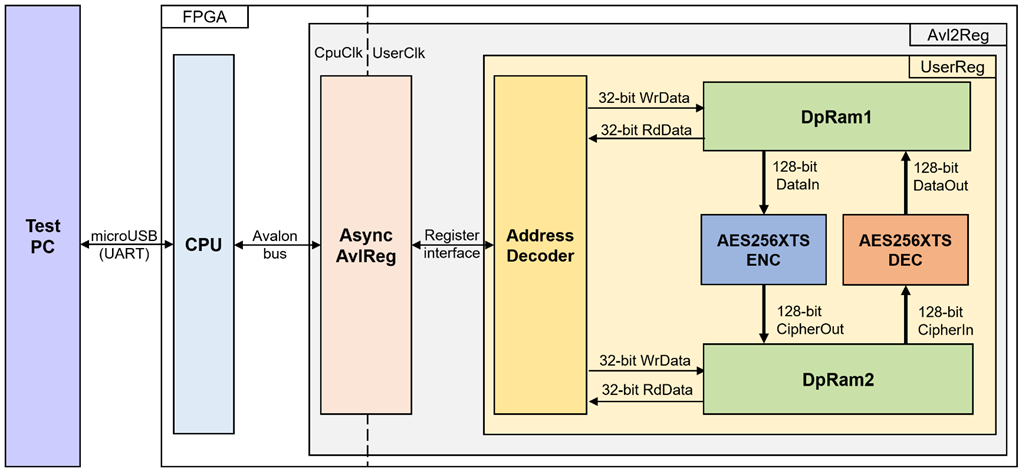
Figure 2‑1 AES256XTSIP reference design block diagram
In this test environment, two AES256XTSIP, called AES256XTSENC and AES256XTSDEC, interface with two dual-port RAMs with asymmetric ports, which are DpRam1 and DpRam2, as shown in Figure 2‑1. AES256XTSIP and two RAMs are sub-modules in UserReg module within Avl2Reg. CPU system is designed to interface with FPGA logic through Avalon-MM bus and interface with user through serial console in test PC.
For user control interface, there are registers in UserReg to store parameters from user such as encryption key, tweakable key, Initialization Vector (IV), number of data to encrypt or decrypt. Input parameters are received from user via serial console.
For user data interface, UserReg is designed to be able to write pattern data or read data in RAMs following user’s command. DpRam1 is used to store the plain data from user which will be input data for AES256XTSENC in encryption mode or the decrypted data which is output data from AES256XTSDEC in decryption mode. DpRam2 is used to store the cipher data from user which will be input data for AES256XTSDEC in decryption mode or encrypted data which is output data from AES256XTSENC in encryption mode.
Because CPU system and AES256XTSENC/AES256XTSDEC run in different clock domain, AsyncAvlReg module inside Avl2Reg is designed as asynchronous circuit to support clock-crossing operation. Also, AsyncAvlReg converts Avalon-MM bus signal which is standard bus in CPU system to be register interface. The details of Avl2Reg module are described as follows.
2.1 Avl2Reg
Avl2Reg module is connected to CPU through Avalon-MM bus. The hardware registers are mapped to CPU memory address, as shown in Table 2‑1. The control and status registers for CPU access are designed in Avl2Reg.
Avl2Reg consists of AsyncAvlReg and UserReg. AsyncAvlReg is designed to convert the Avalon-MM signals to be the simple register interface which has 32-bit data bus size (similar to Avalon-MM data bus size). Additionally, as shown in Figure 2-1, there are two clock domains applied in this block, i.e., CpuClk which is used to interface with CPU through Avalon-MM bus and UserClk which is user clock domain for AES256XTSENC/AES256XTSDEC. AsyncAvlReg includes asynchronous circuit between CpuClk and UserClk.
UserReg includes the register file of the parameters and the status signals of test logics, including dual-port rams and AES256XTSIP. Both data interface and control interface of AES256XTSIP are connected to UserReg. More details of AsyncAvlReg and UserReg are described as follows.
2.2 AsyncAvlReg
This module is designed to convert the signal interface of Avalon-MM to be register interface. Also, it enables two clock domains, CpuClk and UserClk domain, to communicate.
To write register, RegWrEn is asserted to ‘1’ with the valid signal of RegAddr (Register address in 32-bit unit), RegWrData (write data of the register), and RegWrByteEn (the byte enable of this access: bit[0] is write enable for RegWrData[7:0], bit[1] is used for RegWrData[15:8], …, and bit[3] is used for RegWrData[31:24]).
To read register, AsyncAvlReg asserts RegRdReq=’1’ with the valid value of RegAddr (the register address in 32-bit unit). After that, the module waits until RegRdValid is asserted to ‘1’ to get the read data through RegRdData signal at the same clock.
2.3 UserReg
This module is designed to write/read data in RAMs, control and check status of AES256XTSENC and AES256XTSDEC corresponding with write register access or read register request from AsyncAvlReg module. Memory map inside UserReg module is shown in Table 2‑1. Timing diagram of register interface is shown in Figure 2‑2.
Table 2‑1 Register map Definition
|
Address offset |
Register Name |
Rd/Wr |
Description |
|
0x0000 |
ADDR_A1_REG |
Rd/Wr |
[10:4] – address A of DpRam1 (rAddrA1[10:4]). |
|
0x0004 |
ADDR_A2_REG |
Rd/Wr |
[10:4] – address A of DpRam2 (rAddrA2[10:4]). |
|
0x0010 |
ENC_DATAINCNT_REG |
Rd |
[2] – AES256XTSENC EKeyIn busy flag (wEncEKeyInBusy). |
|
Wr |
[15:0] – length of plain data for encryption (rEncDataInCnt[15:0]). rEncStart is asserted to ‘1’ and encryption process is started. |
||
|
0x0014 |
DEC_DATAINCNT_REG |
Rd |
[2] – AES256XTSDEC EKeyIn busy flag (wDecEKeyInBusy). |
|
Wr |
[15:0] – length of cipher data for decryption (rDecDataInCnt[15:0]). rDecStart is asserted to ‘1’ and decryption process is started. |
||
|
0x0018 |
ENC_VER_REG |
Rd |
[31:0] – AES256XTSENC IP version (wEncVersion). |
|
0x001C |
DEC_VER_REG |
Rd |
[31:0] – AES256XTSDEC IP version (wDecVersion). |
|
Rd/Wr |
[31:0] – AES256XTSENC Ekey
(rEncEKeyIn[31:0]). |
||
|
0x0024 |
Rd/Wr |
[31:0] – AES256XTSENC Ekey (rEncEKeyIn[63:32]). |
|
|
0x0028 |
ENC_EKEYIN_2_REG |
Rd/Wr |
[31:0] – AES256XTSENC Ekey (rEncEKeyIn[95:64]). |
|
0x002C |
ENC_EKEYIN_3_REG |
Rd/Wr |
[31:0] – AES256XTSENC Ekey (rEncEKeyIn[127:96]). |
|
0x0030 |
ENC_EKEYIN_4_REG |
Rd/Wr |
[31:0] – AES256XTSENC Ekey (rEncEKeyIn[159:128]). |
|
0x0034 |
ENC_EKEYIN_5_REG |
Rd/Wr |
[31:0] – AES256XTSENC Ekey (rEncEKeyIn[191:160]). |
|
0x0038 |
ENC_EKEYIN_6_REG |
Rd/Wr |
[31:0] – AES256XTSENC Ekey (rEncEKeyIn[223:192]). |
|
0x003C |
ENC_EKEYIN_7_REG |
Rd/Wr |
[31:0] – AES256XTSENC Ekey (rEncEKeyIn[255:224]). |
|
0x0040 |
DEC_EKEYIN_0_REG |
Rd/Wr |
[31:0] – AES256XTSDEC Ekey (rDecEKeyIn[31:0]). |
|
0x0044 |
DEC_EKEYIN_1_REG |
Rd/Wr |
[31:0] – AES256XTSDEC Ekey (rDecEKeyIn[63:32]). |
|
0x0048 |
DEC_EKEYIN_2_REG |
Rd/Wr |
[31:0] – AES256XTSDEC Ekey (rDecEKeyIn[95:64]). |
|
0x004C |
DEC_EKEYIN_3_REG |
Rd/Wr |
[31:0] – AES256XTSDEC Ekey (rDecEKeyIn[127:96]). |
|
0x0050 |
DEC_EKEYIN_4_REG |
Rd/Wr |
[31:0] – AES256XTSDEC Ekey (rDecEKeyIn[159:128]). |
|
0x0054 |
DEC_EKEYIN_5_REG |
Rd/Wr |
[31:0] – AES256XTSDEC Ekey (rDecEKeyIn[191:160]). |
|
0x0058 |
DEC_EKEYIN_6_REG |
Rd/Wr |
[31:0] – AES256XTSDEC Ekey (rDecEKeyIn[223:192]). |
|
0x005C |
DEC_EKEYIN_7_REG |
Rd/Wr |
[31:0] – AES256XTSDEC Ekey (rDecEKeyIn[255:224]). |
|
0x0060 |
ENC_TKEYIN_0_REG |
Rd/Wr |
[31:0] – AES256XTSENC Tkey (rEncTKeyIn[31:0]). |
|
0x0064 |
ENC_TKEYIN_1_REG |
Rd/Wr |
[31:0] – AES256XTSENC Tkey (rEncTKeyIn[63:32]). |
|
0x0068 |
ENC_TKEYIN_2_REG |
Rd/Wr |
[31:0] – AES256XTSENC Tkey (rEncTKeyIn[95:64]). |
|
0x006C |
ENC_TKEYIN_3_REG |
Rd/Wr |
[31:0] – AES256XTSENC Tkey (rEncTKeyIn[127:96]). |
|
0x0070 |
ENC_TKEYIN_4_REG |
Rd/Wr |
[31:0] – AES256XTSENC Tkey (rEncTKeyIn[159:128]). |
|
0x0074 |
ENC_TKEYIN_5_REG |
Rd/Wr |
[31:0] – AES256XTSENC Tkey (rEncTKeyIn[191:160]). |
|
0x0078 |
ENC_TKEYIN_6_REG |
Rd/Wr |
[31:0] – AES256XTSENC Tkey (rEncTKeyIn[223:192]). |
|
0x007C |
ENC_TKEYIN_7_REG |
Rd/Wr |
[31:0] – AES256XTSENC Tkey (rEncTKeyIn[255:224]). |
|
0x0080 |
DEC_TKEYIN_0_REG |
Rd/Wr |
[31:0] – AES256XTSDEC Tkey (rDecTKeyIn[31:0]). |
|
0x0084 |
DEC_TKEYIN_1_REG |
Rd/Wr |
[31:0] – AES256XTSDEC Tkey (rDecTKeyIn[63:32]). |
|
0x0088 |
DEC_TKEYIN_2_REG |
Rd/Wr |
[31:0] – AES256XTSDEC Tkey (rDecTKeyIn[95:64]). |
|
0x008C |
DEC_TKEYIN_3_REG |
Rd/Wr |
[31:0] – AES256XTSDEC Tkey (rDecTKeyIn[127:96]). |
|
0x0090 |
DEC_TKEYIN_4_REG |
Rd/Wr |
[31:0] – AES256XTSDEC Tkey (rDecTKeyIn[159:128]). |
|
0x0094 |
DEC_TKEYIN_5_REG |
Rd/Wr |
[31:0] – AES256XTSDEC Tkey (rDecTKeyIn[191:160]). |
|
0x0098 |
DEC_TKEYIN_6_REG |
Rd/Wr |
[31:0] – AES256XTSDEC Tkey (rDecTKeyIn[223:192]). |
|
0x009C |
DEC_TKEYIN_7_REG |
Rd/Wr |
[31:0] – AES256XTSDEC Tkey (rDecTKeyIn[255:224]). |
|
0x00A0 |
Rd/Wr |
[31:0] – AES256XTSENC IV (rEncIvIn[31:0]). |
|
|
0x00A4 |
ENC_IVIN_1_REG |
Rd/Wr |
[31:0] – AES256XTSENC IV (rEncIvIn[63:32]). |
|
0x00A8 |
ENC_IVIN_2_REG |
Rd/Wr |
[31:0] – AES256XTSENC IV (rEncIvIn[95:64]). |
|
0x00AC |
ENC_IVIN_3_REG |
Rd/Wr |
[31:0] – AES256XTSENC IV (rEncIvIn[127:96]). |
|
0x00C0 |
DEC_IVIN_0_REG |
Rd/Wr |
[31:0] – AES256XTSDEC IV (rDecIvIn[31:0]). |
|
0x00C4 |
DEC_IVIN_1_REG |
Rd/Wr |
[31:0] – AES256XTSDEC IV (rDecIvIn[63:32]). |
|
0x00C8 |
DEC_IVIN_2_REG |
Rd/Wr |
[31:0] – AES256XTSDEC IV (rDecIvIn[95:64]). |
|
0x00CC |
DEC_IVIN_3_REG |
Rd/Wr |
[31:0] – AES256XTSDEC IV (rDecIvIn[127:96]). |
|
0x2000~ |
PLAIN_BASE_ADDR |
Rd/Wr |
[31:0] – Plain data in DpRam1 (wRdDataB1). |
|
0x4000~ |
CIPHER_BASE_ADDR |
Rd/Wr |
[31:0] – Cipher data in DpRam2 (wRdDataB2). |
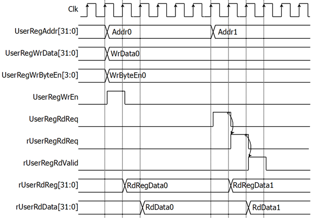
Figure 2‑2 Register interface timing diagram
To read register, the multiplexer is designed to select the read data within each address area. UserRegAddr[10:2] is applied in each register area to select the data. Next, the address decoder uses UserRegAddr[15:13] to select the read data from each area for returning to CPU. As shown in Figure 2‑2, read data is valid in next two clock cycles. When UserRegRdReq is active, rUserRegRdReq is asserted to ‘1’. Then rUserRdValid is active with the valid read value of UserRegAddr.
To write register, UserRegWrEn is asserted to ‘1’ with the valid of UserRegAddr. UserRegAddr[15:13] is used to decode that CPU accesses dual-port ram (DpRam) or internal register area. When CPU accesses DpRam (UserRegAddr[15:13]=“001” or “010”), UserRegAddr[12:2] is set to be the address of DpRam. For example, when UserRegAddr[15:0]=0x2004 and UserRegWrEn=’1’, DpRam1 will be filled with UserRegWrData at Address 0x01. Otherwise, UserRegWrData is loaded to internal register which has matched UserRegAddr[10:0]. For example, rAddrA1 is loaded by UserRegWrData when UserRegAddr=0x0000.
UserRegWrByteEn signal is used when CPU firmware needs to access DpRam by using 64-bit, 32-bit, 16-bit or 8-bit pointer. UserRegWrByteEn[3:0] is mapped to Byte Write Enable port of DpRam.
In this reference design, there are three main operations which are parameter setting, encryption and decryption. Each operation is described as follows.
2.3.1 Encryption key setting
For AES256XTSENC encryption key setting, rEncEKeyIn is set by writing register UserRegAddr=0x0020-0x003F as shown in Table 2‑1. When ENC_EKEYIN_0_REG is written (UserRegAddr=0x0020), rEncEKeyIn[31:0] is set. Then rEncEKeyInValid is asserted to ‘1’ as shown in Figure 2‑3. AES256XTSENC encryption key setting takes 14 clocks cycles to finish.
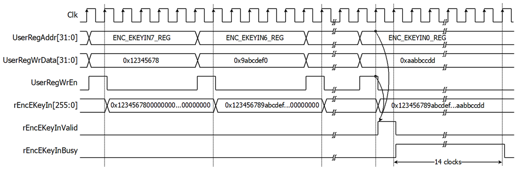
Figure 2‑3 Timing diagram of AES256XTSENC encryption key setting process
For AES256XTSDEC encryption key setting, rDecEKeyIn is set by writing register UserRegAddr=0x0040-0x005F as shown in Table 2‑1. When DEC_EKEYIN_0_REG is written (UserRegAddr=0x0040), rDecEKeyIn[31:0] is set. Then rDecEKeyInValid is asserted to ‘1’ as shown in Figure 2‑4. AES256XTSDEC encryption key setting takes 14 clocks cycles to finish.
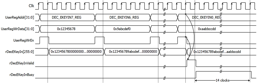
Figure 2‑4 Timing diagram of AES256XTSDEC decryption key setting process
2.3.2 Tweakable key setting
For AES256XTSENC tweakable key setting, rEncTKeyIn is set by writing register UserRegAddr=0x0060-0x007F as shown in Table 2‑1. When ENC_TKEYIN_0_REG is written (UserRegAddr=0x0060), rEncTKeyIn[31:0] is set. Then rEncTKeyInValid is asserted to ‘1’ as shown in Figure 2‑3. AES256XTSENC tweakable key setting takes 14 clocks cycles to finish.
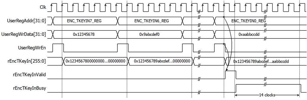
Figure 2‑5 Timing diagram of AES256XTSENC tweakable key setting process
For AES256XTSDEC tweakable key setting, rDecTKeyIn is set by writing register UserRegAddr=0x0080-0x009F as shown in Table 2‑1. When DEC_TKEYIN_0_REG is written (UserRegAddr=0x0080), rDecTKeyIn[31:0] is set. Then rDecTKeyInValid is asserted to ‘1’ as shown in Figure 2‑4. AES256XTSDEC tweakable key setting takes 14 clocks cycles to finish.
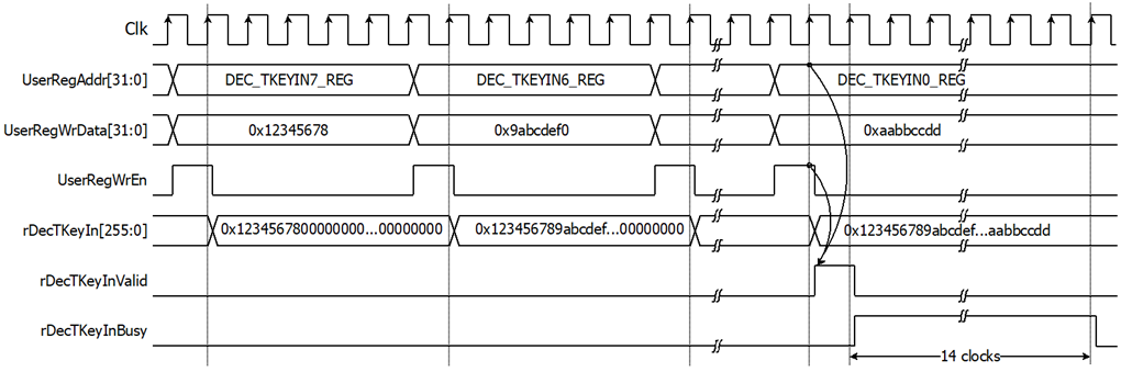
Figure 2‑6 Timing diagram of AES256XTSDEC tweakable key setting process
2.3.3 parameter setting
For encryption process, encryption IV is set by writing ENC_IVIN_0_REG to ENC_IVIN_3_REG. plain data, which will be input data for AES256XTSENC, are stored in DpRam1. Before starting encryption process, address A of DpRam1 (rAddrA1) is set to 0x00 to access the first plain data. Encrypted data from AES256XTSENC is stored in DpRam2. Before starting encryption process, address A of DpRam2 (rAddrA2) is set to 0x00 for writing the first output encrypted data. For setting length of plain data, rEncDataInCnt, ENC_DATAINCNT_REG is written and then rEncStart is asserted to ‘1’ to start encryption as shown in Figure 2‑7.
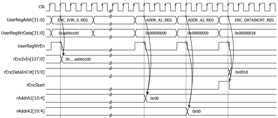
Figure 2‑7 Timing diagram example of encryption parameter setting
For decryption process, decryption IV is set by writing DEC_IVIN_0_REG to DEC_IVIN_3_REG. cipher data, which will be input data for AES256XTSDEC, are stored in DpRam2. Before starting decryption process, address A of DpRam2 (rAddrA2) is set to 0x00 to access the first cipher data. Decrypted data from AES256XTSDEC is stored in DpRam1. Before starting decryption process, address A of DpRam1 (rAddrA1) is set to 0x00 for writing the first output decrypted data. For setting length of cipher data, rDecDataInCnt, DEC_DATAINCNT_REG is written and then rDecStart is asserted to ‘1’ to start decryption as shown in Figure 2‑8.

Figure 2‑8 Timing diagram example of decryption parameter setting
2.3.4 Encryption
For encryption process, 128-bit plain data, which will be input data for AES256XTSENC, are stored in DpRam1. Before starting encryption process, address A of DpRam1 (rAddrA1) is set to 0x00 to access the first plain data. DpRam1 has wRdEnA1 as the read enable signal of the ram and wRdEnA1 is asserted to ‘1’ when rEncStart=‘1’ or wEncDataInRd=‘1’. As shown in Figure 2‑9, when wRdEnA1 is active, rAddrA1 is increased by 1 to access next 128-bit plain data.
Before starting encryption process, address A of DpRam2 (rAddrA2) is set to 0x00 for writing the first encrypted data. When wEncDataOutValid is active, wEncDataOut is loaded to DpRam2. Then rAddrA2 is increased by 1 prepared for next encrypted output as shown in Figure 2‑9.
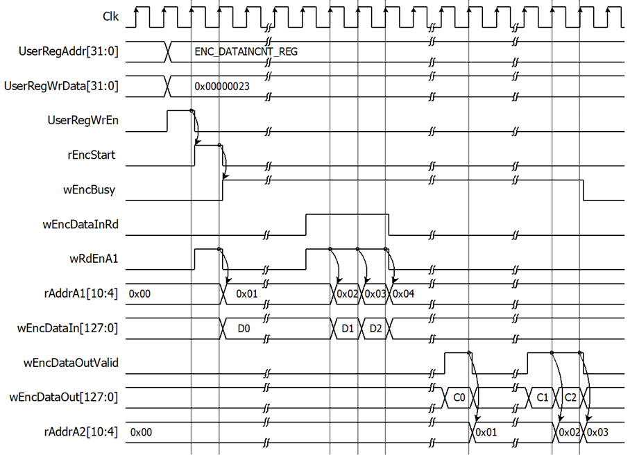
Figure 2‑9 : Example of a 35-byte data encryption timing diagram
2.3.5 Decryption
For decryption process, 128-bit cipher data, which will be input data for AES256XTSDEC, are stored inDpRam2. Before starting decryption process, address A of DpRam2 (rAddrA2) is set to 0x00 to access the first cipher data. DpRam2 has wRdEnA2 as the read enable signal of the ram and wRdEnA2 is asserted to ‘1’ when rDecStart=‘1’ or wDecDataInRd=‘1’. As shown in Figure 2‑10, when wRdEnA2 is active, rAddrA2 is increased by 1 to access next 128-bit cipher data.
Before starting decryption process, address A of DpRam1 (rAddrA1) is set to 0x00 for writing the first decrypted data. When wDecDataOutValid is active, wDecDataOut is loaded to DpRam1. Then rAddrA1 is increased by 1 prepared for next decrypted output as shown in Figure 2‑10.
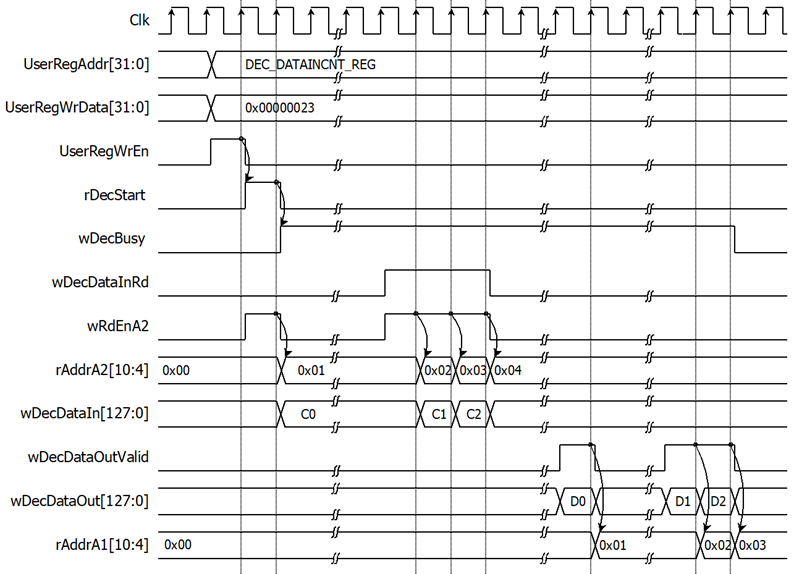
Figure 2‑10 Example of a 35-byte data decryption timing diagram
3 CPU Firmware
After system boot-up, CPU initializes its peripherals such as UART and Timer and shows IP version of AES256XTSIP. Then main menu is displayed. Main function runs in an infinite loop to show the main menu and get keyboard input from user. User can select each menu via serial console that will call the related functions. After functions finished running, the main menu is displayed again. More details of the sequence in each menu are described as follows.
3.1 Set encryption key
This menu is used to set encryption key for encryption module and decryption module. set_key_or_iv function is called to change Ekey set. User can input “enter” key to skip input Ekey and not change current key for encryption module or to skip input Ekey and change key similar to encryption module for decryption module. ENC_EKEYIN_0_REG, DEC_EKEYIN_0_REG, 64-character, “rEncEKeyIn”, “rDecEKeyIn” are input parameters. set_key_or_iv function is described in Table 3‑1.
Table 3‑1 set_key_or_iv function
|
void set_key_or_iv(unsigned int *enc_addr, unsigned int *dec_addr, unsigned int length_hex, char *enc_label, char *dec_label) |
|
|
Parameter |
enc_addr: register for set key or iv of encryption module dec_addr: register for set key or iv of decryption module length_hex: length character of key or iv enc_label: name of signal for encryption module dec_label: name of signal for decryption module |
|
Return value |
None |
|
Description |
This function displays current key or iv on the console. Receive input new key or iv in hexadecimal format or “enter” key to skip. User’s input will be ignored if it is not hexadecimal format. Then the function monitors busy status until busy status is not active. Then set the registers. |
3.2 Set tweakable key
This menu is used to set tweakable key for encryption module and decryption module. set_key_or_iv function is called to change Tkey set. User can input “enter” key to skip input Tkey and not change current key for encryption module or to skip input Tkey and change key similar to encryption module for decryption module. ENC_TKEYIN_0_REG, DEC_TKEYIN_0_REG, 64-character, “rEncTKeyIn”, “rDecTKeyIn” are input parameters.
3.3 Set encryption/decryption IV
This menu is used to set Initialization Vector (IV) for encryption module and decryption module. set_key_or_iv function is called to change iv set. User can input “enter” key to skip input iv and not change current key for encryption module or to skip input iv and change key similar to encryption module for decryption module. ENC_IVIN_0_REG, DEC_IVIN_0_REG, 32-character, “rEncIvIn”, “rDecIvIn” are input parameters.
3.4 Show Data Memory
This menu is used to show data in memory. User can set the number of data to show on console in byte unit. The sequence of the firmware is as follows.
1) Receive the length of data in decimal format or “enter” key to use default value. The length of data to show is stored in length.
2) Call show_data function to show data in memory with PLAIN_BASE_ADDR and length as input parameters. show_data function is described in Table 3‑2.
Table 3‑2 show_data function
|
void show_data(unsigned int base_addr, unsigned int length) |
|
|
Parameter |
base_addr: base address to access memory length: length of data to show |
|
Return value |
None |
|
Description |
This function shows data in both DpRam1 and DpRam2 corresponding to length. CPU firmware reads data in DpRam1, starting at PLAIN_BASE_ADDR, and shows on console. Also, CPU firmware reads data in DpRam2, starting at CIPHER_BASE_ADDR, and shows on console. If length is too large, length will be set to the size of memory. |
3.5 Fill Plain Data Memory
This menu is used to fill DpRam1 with plain data pattern. The sequence of the firmware is as follows.
1) Receive the length of plain data in decimal format or “enter” key to set length of data to default value. If user input less than 16 bytes, the length of data will be 16 bytes. The number of data to encrypt is stored in enc_data_cnt.
2) Call fill_data function to choose data pattern and fill DpRam1 with selected pattern. The input parameter of fill_data is PLAIN_BASE_ADDR which is base address for DpRam1 and enc_data_cnt.
3) Call show_data function to show data in both DpRam1 and DpRam2 corresponding to enc_data_cnt.
According to Table 3‑3, there are four data pattern choices to fill memory that are zero pattern, 8-bit counter pattern, 16-bit counter pattern and 32-bit counter pattern. For zero pattern, user can select this choice to clear data memory. It makes user see the output of encryption/decryption more clearly.
Table 3‑3 fill_data function
|
void fill_data(unsigned int base_addr, unsigned int data_length) |
|
|
Parameter |
base_addr: base address to access memory data_length: length of data to fill data pattern |
|
Return value |
None |
|
Description |
This function fills the selected pattern in memory corresponding to base_addr. Before filling memory, the function shows data pattern choices on serial console and waits for user’s input. For invalid choice, the console will display the error message and wait until user input new valid choice. Then selected data pattern is filled into memory by the length of data (data length) and filled zeros into the remaining memory from address base_addr+0x0000 to base_addr+0x1FFF. |
3.6 Encrypt
This menu is used to start encryption process with current encryption parameters. The sequence of the firmware is as follows.
1) Call aes_command function to set the starting address, number of data to encrypt and check status. ENC_CNT_REG and enc_data_cnt are input parameters. aes_command function is described in Table 3-7.
2) Print plain data length and call show_data function to show data in memory by the number of plain data.
Table 3-7 aes_command function
|
void aes_command(unsigned int *DATACNT_REG, unsigned int data_cnt) |
|
|
Parameter |
DATACNT_REG: register for data length data_cnt: the number of data to operate |
|
Return value |
None |
|
Description |
This function sets the starting address of DpRam1 and DpRam2 by writing register ADDR_A1_REG and ADDR_A2_REG, respectively. Then DATACNT_REG is written with data_cnt to set the number of data to operate. Also, DATACNT_REG is monitored to check whether operation finish. When operation finished, *DATACNT_REG=0 which means AES256XTSIP is not busy. |
3.7 Fill Cipher Data Memory
This menu is used to fill DpRam2 with cipher data pattern. The sequence of the firmware is as follows.
1) Receive the length of cipher data in decimal format or “enter” key to set length of data to default value. If user input less than 16 bytes, the length of data will be 16 bytes. The number of data to decrypt is stored in dec_data_cnt.
2) Call fill_data function to choose data pattern and fill DpRam2 with selected pattern. The input parameter of fill_data is CIPHER_BASE_ADDR which is base address for DpRam2 and dec_data_cnt.
3) Call show_data function to show data in both DpRam1 and DpRam2 corresponding to dec_data_cnt.
3.8 Decrypt
This menu is used to start decryption process with current decryption parameters. The sequence of the firmware is as follows.
1) Call aes_command function to set the starting address, number of data to decrypt and check status. DEC_CNT_REG and dec_data_cnt are input parameters.
2) Print cipher
data length and call show_data function to show data in memory by the number of
cipher data.
4 Revision History
|
Revision |
Date |
Description |
|
1.00 |
30-Nov-2022 |
Initial version release |