ChaCha20Poly1305-IP Reference Design
2.3.3 Encryption/Decryption/Bypass Operation
3.2 Set Encryption/Decryption Key
3.3 Set Encryption/Decryption IV
1 Introduction
This document describes the detail of ChaCha20Poly1305-IP reference design. In this reference design, ChaCha20Poly1305-IP is used to encrypt and decrypt data between two memories in FPGA and provide authentication tag. User can fill memory with Additional Authenticated Data (AAD), plain or cipher data, set encryption/decryption key, Initialization Vector (IV), and control the test operation and monitor results via serial console on a test PC. More details of the hardware design and CPU firmware are described as follows.
2 Hardware Overview
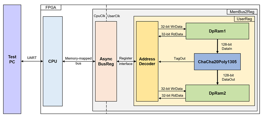
Figure 1 ChaCha20Poly1305-IP reference design block diagram
In this test environment, the ChaCha20Poly1305-IP interface with two dual-port RAMs with asymmetric ports, which are DpRam1 and DpRam2, as shown in Figure 1. ChaCha20Poly1305-IP and two RAMs are sub-modules in UserReg module within MemBus2Reg. CPU system is designed to interface with FPGA logic through memory-mapped bus (AXI4-Lite) and interface with user through serial console in test PC.
For user control interface, there are registers in UserReg to store parameters from user such as encryption and decryption keys, initialization vector (IV), the number of AAD and data to encrypt or decrypt. Input parameters are received from user via serial console.
For user data interface, UserReg is designed to be able to write or read data in RAMs following user’s command and read authentication tag. DpRam1 is used to store AAD and the DataIn from user which will be input data for ChaCha20Poly1305-IP. DpRam2 is used to store output data from ChaCha20Poly1305-IP. Authentication tag is stored in registers which user can read.
Because CPU system and ChaCha20Poly1305-IP run in different clock domain, AsyncBusReg module inside MemBus2Reg is designed as asynchronous circuit to support clock-crossing operation. Also, AsyncBusReg converts memory-mapped bus signal which is standard bus in CPU system to be register interface. The details of MemBus2Reg module are described as follows.
2.1 MemBus2Reg Module
The MemBus2Reg module interfaces with the CPU through a memory-mapped bus, such as AXI4-Lite. The hardware registers within MemBus2Reg are mapped to specific CPU memory addresses, as shown in Table 1. These registers include control and status registers that enable the CPU to access and manage the module.
MemBus2Reg consists of two main sub-modules: AsyncBusReg and UserReg. The AsyncBusReg sub-module is responsible for converting the signals from the memory-mapped bus into a simple register interface that uses a 32-bit data bus, maintaining consistency with the bus’s data size. As shown in Figure 1, the MemBus2Reg module operates with two clock domains: CpuClk, which interfaces with the CPU, and UserClk, which operates in the user-defined clock domain. The AsyncBusReg sub-module includes circuitry to handle asynchronous communication between these two clock domains.
2.2 AsyncBusReg
This module is designed to convert the signal interface of a memory-mapped bus into a register interface. Also, it enables two clock domains, CpuClk and UserClk domain, to communicate.
To write register, RegWrEn is asserted to ‘1’ with the valid signal of RegAddr (Register address in 32-bit unit), RegWrData (write data of the register), and RegWrByteEn (the byte enable of this access: bit[0] is write enable for RegWrData[7:0], bit[1] is used for RegWrData[15:8], …, and bit[3] is used for RegWrData[31:24]).
To read register, AsyncBusReg asserts RegRdReq=‘1’ with the valid value of RegAddr (the register address in 32-bit unit). After that, the module waits until RegRdValid is asserted to ‘1’ to get the read data through RegRdData signal at the same clock.
2.3 UserReg
This module is designed to write/read data in RAMs, read tag, control and check status of ChaCha20Poly1305-IP corresponding with write register access or read register request from AsyncBusReg module. Memory map inside UserReg module is shown in Table 1. Timing diagram of register interface is shown in Figure 2.
Table 1 Register map Definition
|
Address offset |
Register Name |
Rd/Wr |
Description |
|
0x0000 |
STATUS_ADDR |
Rd |
[0] – ChaCha20Poly130-IP busy flag (!rOperationEn). |
|
0x0100 |
PARAMS_ADDR |
Rd/Wr |
[2] – Enable
Speed test mode (rSpeedTestEn). |
|
0x0200 |
AAD_CNT_ADDR0 |
Rd/Wr |
[31:0] – length of AAD for encryption/decryption (rAadCnt [31:0]). |
|
0x0204 |
AAD_CNT_ADDR1 |
Rd/Wr |
[31:0] – length of AAD for encryption/decryption (rAadCnt [63:32]). |
|
0x0300 |
DATA_CNT_ADDR0 |
Rd/Wr |
[31:0] – length of Plaintext or Ciphertext (rDataCnt [31:0]). |
|
0x0304 |
DATA_CNT_ADDR1 |
Rd/Wr |
[31:0] – length of Plaintext or Ciphertext (rDataCnt [63:32]). |
|
0x0400 |
INPUT_RD_ADDR |
Wr |
[0] – Set rOperationEn to ‘1’ then KeyValid will be asserted when KeyReady = ‘1’ to start operation. |
|
0x0500 |
KEY_IN_ADDR0 |
Rd/Wr |
[31:0] – Encryption/Decryption key (rKeyIn[31:0]). |
|
0x0504 |
KEY_IN_ADDR1 |
Rd/Wr |
[31:0] – Encryption/Decryption key (rKeyIn[63:32]). |
|
0x0508 |
KEY_IN_ADDR2 |
Rd/Wr |
[31:0] – Encryption/Decryption key (rKeyIn[95:64]). |
|
0x050C |
KEY_IN_ADDR3 |
Rd/Wr |
[31:0] – Encryption/Decryption key (rKeyIn[127:96]). |
|
0x0510 |
KEY_IN_ADDR4 |
Rd/Wr |
[31:0] – Encryption/Decryption key (rKeyIn[159:128]). |
|
0x0514 |
KEY_IN_ADDR5 |
Rd/Wr |
[31:0] – Encryption/Decryption key (rKeyIn[191:160]). |
|
0x0518 |
KEY_IN_ADDR6 |
Rd/Wr |
[31:0] – Encryption/Decryption key (rKeyIn[223:192]). |
|
0x051C |
KEY_IN_ADDR7 |
Rd/Wr |
[31:0] – Encryption/Decryption key (rKeyIn[255:224]). |
|
0x0600 |
IV_IN_ADDR0 |
Rd/Wr |
[31:0] – Encryption/Decryption IV (rIvIn[31:0]). |
|
0x0604 |
IV_IN_ADDR1 |
Rd/Wr |
[31:0] – Encryption/Decryption IV (rIvIn[63:32]). |
|
0x0608 |
IV_IN_ADDR2 |
Rd/Wr |
[31:0] – Encryption/Decryption IV (rIvIn[95:64]). |
|
0x0700 |
TAG_OUT_ADDR0 |
Rd |
[31:0] – Authentication tag (rTagOut[31:0]). |
|
0x0704 |
TAG_OUT_ADDR1 |
Rd |
[31:0] – Authentication tag (rTagOut[63:32]). |
|
0x0708 |
TAG_OUT_ADDR2 |
Rd |
[31:0] – Authentication tag (rTagOut[95:64]). |
|
0x070C |
TAG_OUT_ADDR3 |
Rd |
[31:0] – Authentication tag (rTagOut[127:96]). |
|
0x0800 |
IPVERSION_REG |
Rd |
[31:0] – ChaCha20Poly1305-IP version (wVersion). |
|
0x4000~0x4FFF |
DATA_IN_ADDR |
Rd/Wr |
[31:0] – Data in DpRam1 (wRdDataB1). |
|
0x8000~0x8FFF |
DATA_OUT_ADDR |
Rd/Wr |
[31:0] – Data in DpRam2 (wRdDataB2). |
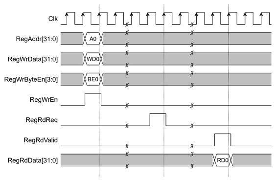
Figure 2 Register interface timing diagram
To read register, one multiplexer is designed to select the read data within each address area. UserRegAddr[10:2] is applied in each register area to select the data. Next, the address decoder uses UserRegAddr[15:11] to select the read data from each area for returning to CPU. As shown in Figure 2, read data is valid in next two clock cycles. When UserRegRdReq is active, rUserRegRdReq is asserted to ‘1’. Then rUserRdValid is active with the valid read value of UserRegAddr.
To write register, UserRegWrEn is asserted to ‘1’ with the valid of UserRegAddr. UserRegAddr[15:11] is used to decode that CPU accesses dual-port ram (DpRam) or internal register area. When CPU accesses DpRam (UserRegAddr[15:11]=“00100” or “01000”), UserRegAddr[10:2] is set to be the address of DpRam. For example, when UserRegAddr[15:0]=0x4004 and UserRegWrEn=’1’, DpRam1 will be filled with UserRegWrData at Address 0x01. Otherwise, UserRegWrData is loaded to internal register which has matched UserRegAddr[10:2]. For example, rAadCnt is loaded by UserRegWrData when UserRegAddr=0x0200.
UserRegWrByteEn signal is used when CPU firmware needs to access DpRam by using 32-bit, 16-bit or 8-bit pointer. UserRegWrByteEn[3:0] is mapped to Byte Write Enable port of DpRam.
In this reference design, there are three main operations which are parameter setting, encryption/decryption/bypass. Each operation is described as follows.
2.3.1 Key/IV Setting
For key configuration, rKeyIn is configured by writing to registers KEY_IN_ADDR7 through KEY_IN_ADDR0, and rIvIn is configured by writing to registers IV_IN_ADDR2 through IV_IN_ADDR0. The timing diagram is shown in
Figure 3.
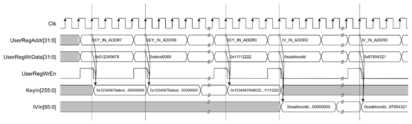
Figure 3 Timing diagram of Key/IV setting process
2.3.2 Parameter Setting
The operation mode is configured through the PARAMS_ADDR register.
· 0x00 : Encryption mode
· 0x01 : Decryption mod
· 0x02 : Bypass mode
· 0x04 : SpeedTest mode
The AAD length is set by writing to AAD_CNT_ADDR0 and AAD_CNT_ADDR1. The Data length is set by writing to DATA_CNT_ADDR0 and DATA_CNT_ADDR1. The timing diagram is shown in Figure 4.
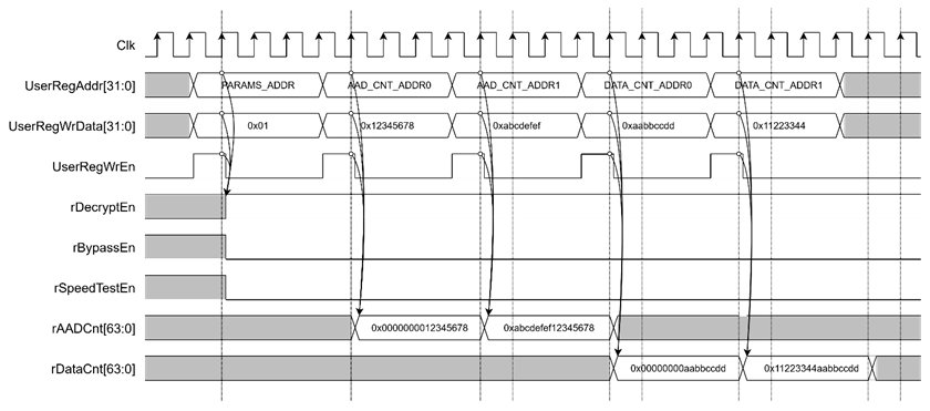
Figure 4 Timing diagram example of parameter setting
2.3.3 Encryption/Decryption/Bypass Operation
For encryption, decryption, or bypass operations, the rDecryptEn, rBypassEn, and rSpeedTestEn registers are used to define the operation type. wAddrB is set to 0x00 to access the first 128-bit block of DataIn. Then, wAddrB increments by 1 to access next 128-bit DataIn blocks from DpRam1. When either wAADOutValid or wDataOutValid becomes active, wDataOut is stored in DpRam2, and rAddrB2 is incremented by 1 to prepare for the next DataOut as shown in Figure 5.
The operation begins by writing ‘1’ to bit 0 of the INPUT_RD_ADDR register (which sets rOperationEn to ‘1’). The signal wKeyInValid becomes active when both rOperationEn and wKeyInReady are ‘1’. Once wKeyInValid is asserted, the ChaCha20Poly1305-IP will be ready to receive data within a few clock cycles.
The authentication tag is stored in a register (rTagOut) after wTagOutValid is active, and the user can access this tag by reading TAG_OUT_ADDR0 to TAG_OUT_ADDR3.
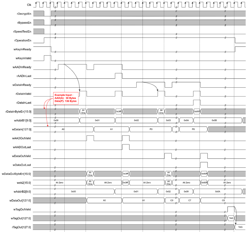
Figure 5 Example timing diagram of encryption mode
Note: For bypass mode, wTagOutValid will not be active, and rTagOut is not valid.
2.3.4 SpeedTest Operation
When the operation begins in SpeedTest mode, wDataIn is fixed at 0, and all control signals such as rDataInValid, rAADInLast, and rDataInLast behave as shown in Figure 6. The wDataCtr signal counts the number of bytes that the IP core receives as DataIn. The rAADInLast and rDataInLast signals become active when their conditions are met, as indicated in the timing diagram.
The authentication tag is calculated using the ChaCha20Poly1305-IP encryption mode, and the user can access this tag by reading from TAG_OUT_ADDR0 to TAG_OUT_ADDR3.
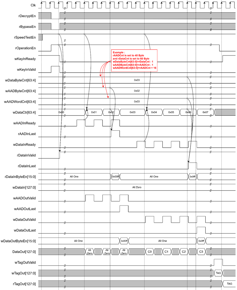
Figure 6 Example timing diagram of SpeedTest mode
3 CPU Firmware
Table 2 init_params function
|
void init_params() |
|
|
Parameter |
None |
|
Return value |
None |
|
Description |
This function initializes the ChaCha20Poly1305-IP with default test parameters from RFC 8439. It writes a 256-bit test key to KEY_IN_ADDR registers, writes a 96-bit test IV to IV_IN_ADDR registers, and fills DATA_IN_ADDR memory with test AAD and input data. The function calculates the number of 16-byte blocks needed for AAD and data, then writes them to memory with proper padding. Length is written to AAD_CNT_ADDR and DATA_CNT_ADDR registers store the data length. |
3.1 Change Mode
This menu is used to set operation mode from user input by writing down PARAMS_ADDR register. If user switches from SPEED TEST mode to any other mode (ENCRYPT/DECRYPT/BYPASS), the firmware automatically calls init_params() to restore default test parameters (key, IV, AAD, and data). This is necessary because SPEED TEST mode only stores data sizes, not actual data values.
3.2 Set Encryption/Decryption Key
This menu is used to set the encryption/decryption key. Prompt user to enter new key value in hexadecimal format. Call getHex() function with KEY_IN_ADDR as base address and maximum length of 64 characters to receive user input. User can press "Enter" to skip input and retain current key. If the user input is less than 256 bits, zero-padding is applied to the remaining key registers.
Table 3 getHex function
|
uint8_t getHex(uint32_t *str, uint64_t *strLen, uint64_t Max_length) |
|
|
Parameter |
str: Pointer to where converted hex values will be stored strLen: Pointer to where the number of bytes written will be stored Max_length: Maximum length allowed for input in hexadecimal characters |
|
Return value |
0: Successful input - user pressed Enter 1: ESC key pressed (cancel operation) |
|
Description |
This function continuously reads hexadecimal characters from UART and stores them in an array until the number of input characters reaches Max_length. The function terminates when Enter or ESC is pressed. When the user presses Enter, the function processes all stored data by taking 4 bytes (8 hex characters) at a time, converting each group to a 32-bit unsigned integer with endian swapping, and storing the results directly in the provided uint32_t *str. If there is an odd number of hex digits, the function pads with '0' on the right. If ESC is pressed, the function terminates without writing any values. |
3.3 Set Encryption/Decryption IV
3.4 Edit AAD & Data Memory
This menu is used to set the length and fill the memory for AAD and input data. The behavior differs based on the current operation mode. The sequence of the firmware is as follows:
For SPEED TEST Mode:
1) Receive the length of AAD in byte unit or "Enter" key to set AAD length to zero.
2) Set AAD count by writing to AAD_CNT_ADDR register.
3) Receive the length of Data in byte unit or "Enter" key to set Data length to zero.
4) Set Data count by writing to DATA_CNT_ADDR register.
For Other Modes (ENCRYPT/DECRYPT/BYPASS):
1) Prompt user to enter AAD value in hexadecimal format. Call getHex() function with DATA_IN_ADDR as base address and maximum length of 16KB to receive user input. User can press "Enter" to set AAD to zero or "ESC" to keep current value.
2) Write AAD length to AAD_CNT_ADDR register. If AAD length is not a multiple of 16 bytes and is non-zero, perform zero-padding to the next 16-byte boundary and calculate aad_pad as the AAD length with zero padding.
3) Prompt user to enter Data value in hexadecimal format. Call getHex() function with DATA_IN_ADDR + aad_pad as base address and data_left ((16KB – aad_pad)*2) as maximum length. User can press "Enter" to set Data to zero or "ESC" to clear current value.
4) Write Data length to DATA_CNT_ADDR register. If Data length is not a multiple of 16 bytes and is non-zero, perform zero-padding to the next 16-byte boundary.
3.5 Show AAD & Data Memory
This menu is used to display the contents of Input Data memory. User can specify the number of bytes to display. The sequence of the firmware is as follows:
1) Check current mode - if in SPEED TEST mode, skip display (return to main menu) as no actual data is stored in this mode.
2) Prompt user to enter the number of bytes to display, or press "Enter" to display all data.
3) Call print_col() function to display memory contents starting from DATA_IN_ADDR with the specified length.
Table 4 print_col function
|
void print_col(const uint8_t *col, const uint64_t col_len) |
|
|
Parameter |
col: Pointer to the data array to display col_len: Number of bytes to display |
|
Return value |
None |
|
Description |
This function displays memory contents in a formatted hexadecimal table. It prints a header row showing column positions (0 through F) in cyan color, followed by rows of data. Each row starts with an 8-digit hexadecimal address offset in cyan, followed by up to 16 bytes of data in hexadecimal format with spacing after every 4 bytes for readability. |
3.6 Execute Operation
This menu is used to start the operation process based on the currently selected mode. The firmware executes encryption, decryption, bypass, or speed test operation.
The sequence is as follows:
1) Start timer.
2) Write 1 to INPUT_RD_ADDR register to signal the ChaCha20Poly1305-IP to begin processing.
3) Poll STATUS_ADDR register continuously, waiting for STATUS_TAG_OUT_VALID bit (bit 0) to become ’1’.
4) When operation completes, stop timer and calculate execution time.
5) Display operation result
For SPEED TEST Mode:
a) Display generated 128-bit authentication tag from TAG_OUT_ADDR registers
b) Show execution time and calculated throughput in Mbps
For Other Modes (ENCRYPT/DECRYPT/BYPASS):
a) Display side-by-side comparison of Input Data and Output Data using print_col_diff() function
b) Display generated 128-bit authentication tag from TAG_OUT_ADDR registers (not applicable in bypass mode)
c) Show execution time and calculated throughput in Mbps
Table 5 print_col_diff function
|
void print_col_diff(const uint8_t *col1, const uint8_t *col2, const uint64_t col_len) |
|
|
Parameter |
col1: Pointer to first byte array (Input Data) col2: Pointer to second byte array (Output Data) col_len: Number of bytes to display |
|
Return value |
None |
|
Description |
This function displays two memory regions side-by-side for comparison. It prints a double-width header showing column positions for both data columns in cyan. Each row begins with an 8-digit hexadecimal address offset in cyan, followed by up to 16 bytes from col1 in hexadecimal format, then spacing, then up to 16 bytes from col2 with the same formatting. This allows direct visual comparison between input and output data. |
4 Revision History
|
Revision |
Date (D-M-Y) |
Description |
|
1.00 |
14-Oct-25 |
Initial version release |