ChaCha20Poly1305Lite-IP Demo Instruction
2 FPGA Development Board Setup
4 Command Details and Test Results
1 Environment Setup
To operate ChaCha20Poly1305Lite-IP demo, please prepare the following test environment.
1) FPGA development board
2) Test PC.
3) Micro USB cable for JTAG connection between FPGA board and Test PC.
4) Quartus programmer for programming FPGA and Nios command shell, installed on PC.
5) Demo configuration file (To download this file, please visit our web site at www.design-gateway.com).
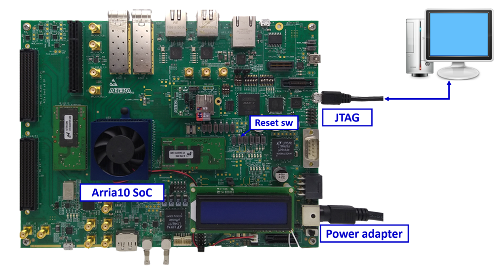
Figure 1 ChaCha20Poly1305Lite-IP demo environment on Arria10 SoC board
2 FPGA Development Board Setup
1) Make sure power switch is off and connect power supply to FPGA development board.
2) Connect USB cables between FPGA board and PC via micro-USB ports.
3) Turn on power switch for FPGA board.
4) Open Quartus Programmer to program FPGA through USB-1 by following step.
i). Click “Hardware Setup…” to select USB-BlasterII [USB-1]
ii). Click “Auto Detect” and select FPGA number.
iii). Select FPGA device icon.
iv). Click “Change File” button, select SOF file in pop-up window and click “open” button.
v). Check “program”.
vi). Click “Start” button to program FPGA.
vii). Wait until Progress status is equal to 100%.
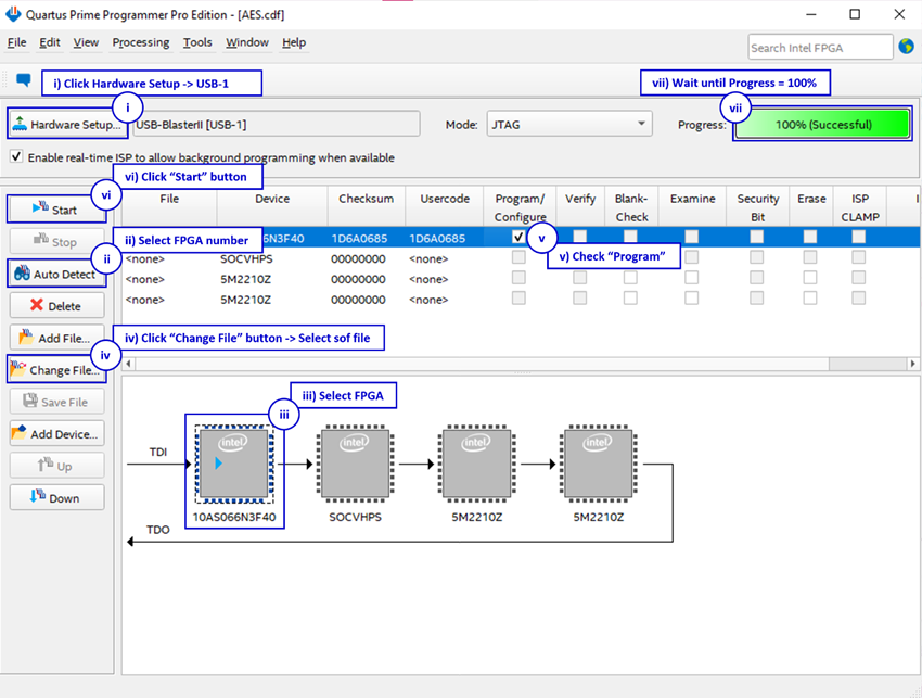
Figure 2 Program Device
For A10SoC, after the SOF file has been programmed, Quartus Prime will show popup message of Intel FPGA IP Evaluation Mode Status as shown in Figure 3. Please do not press cancel button.
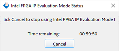
Figure 3 Intel FPGA IP Evaluation Mode Status
3 Nios Command Shell
User can fill RAMs with AAD, IV, Input Data, and encryption/decryption key via Nios II Command Shell. The current parameters are shown together with the available options in the main menu as shown in Figure 4. The details of each menu are described in topic 4.
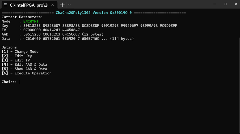
Figure 4 Main menu on Nios II Command Shell
4 Command Details and Test Results
4.1 Change Mode
Select “Change Mode” from the main menu to switch the ChaCha20Poly1305Lite-IP operation mode. The available options are shown in Figure 5.
1) ENCRYPT: Encrypts Input Data stored in memory.
2) DECRYPT: Decrypts Input Data stored in memory.
3) BYPASS: Bypasses Input Data stored in memory without encryption or decryption.
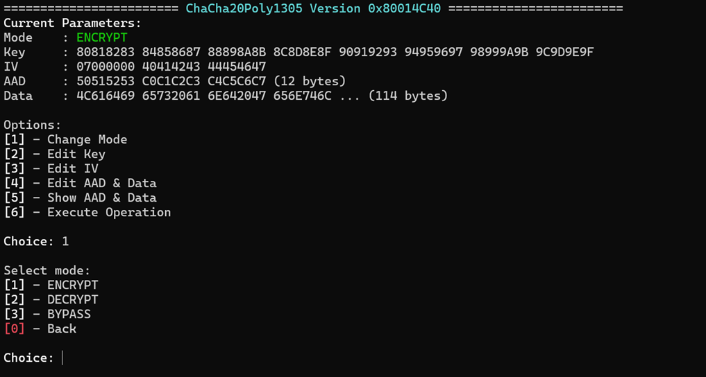
Figure 5 Change Mode Menu
4.2 Edit key
The steps to edit key are as follows
1) Select “Edit Key”.
2) Enter up to 256-bit key value in hexadecimal format as shown in Figure 6.
3) After pressing Enter, the new key value will be updated and displayed in the main menu.
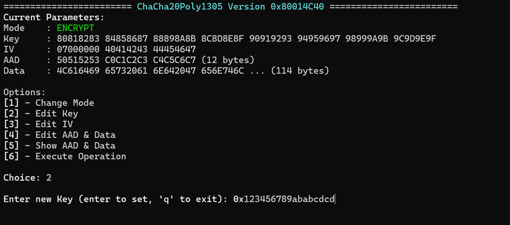
Figure 6 Key setting example
4.3 Edit IV
The steps to edit IV are as follows
1) Select “Edit IV”.
2) Enter up to 96-bit IV value in hexadecimal format as shown in Figure 7.
3) After pressing Enter, the new IV value will be updated and displayed in the main menu.
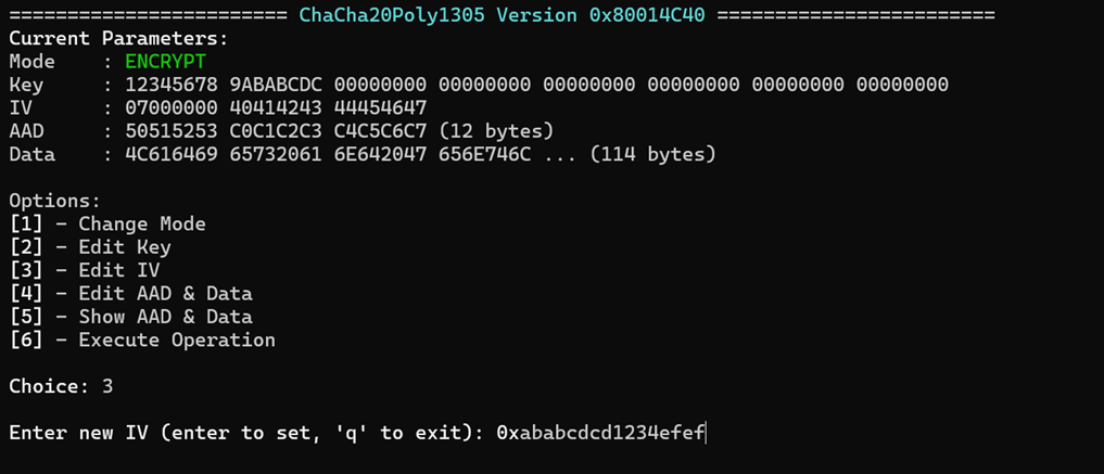
Figure 7 IV setting example
4.4 Edit AAD & Data
Select “Edit AAD & Data” to update AAD and Data in memory. Users must update both AAD and Data in this menu.
1) Enter AAD value in hexadecimal and press Enter.
2) Enter Data value in hexadecimal as shown in Figure 8 and press Enter.
3) After both inputs, the new values and sizes are updated and shown in the main menu.
Notes:
· Combined AAD + Data size cannot exceed 16 KB.
· In Decrypt mode, Data is treated as Ciphertext; in Encrypt mode, it is Plaintext.
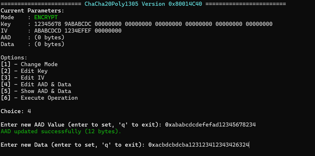
Figure 8 AAD & Data setting example
4.5 Show AAD & Data
The steps to show AAD & Data in memory are as follows:
1) Select “Show AAD & Data”
2) Enter the number of bytes to display (or press Enter to display all).
3) The AAD and Data values are shown in table form as shown in Figure 9.
4) After pressing Enter, the console will return to the main menu.
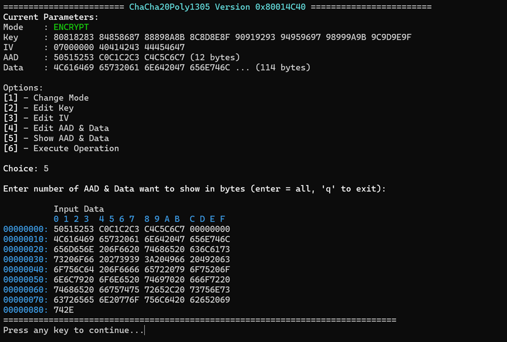
Figure 9 Show AAD & Data example
4.6 Execute Operation
Select “Execute Operation” to start the operation in the currently selected mode.
4.6.1 Encrypt
In Encrypt mode, the IP uses the current key and IV to encrypt the Input Data in memory. The Output Data (Ciphertext) and 128-bit authentication tag are displayed as shown in Figure 10.
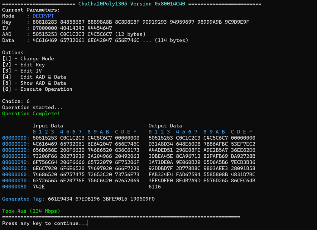
Figure 10 Encryption Mode result
4.6.2 Decrypt
In Decrypt mode, the IP uses the current key and IV to decrypt the Input Data in memory. The Output Data (recovered Plaintext) and the 128-bit authentication tag are displayed as shown in Figure 11.
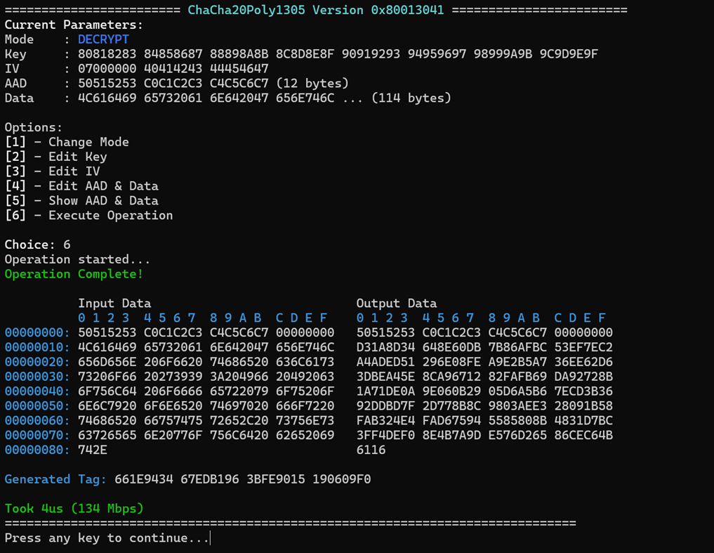
Figure 11 Decryption Mode result
4.6.3 Bypass
In Bypass mode, the IP simply passes the Input Data from memory to output memory without any encryption or decryption. Both Input Data and Output Data are displayed as shown in Figure 12.
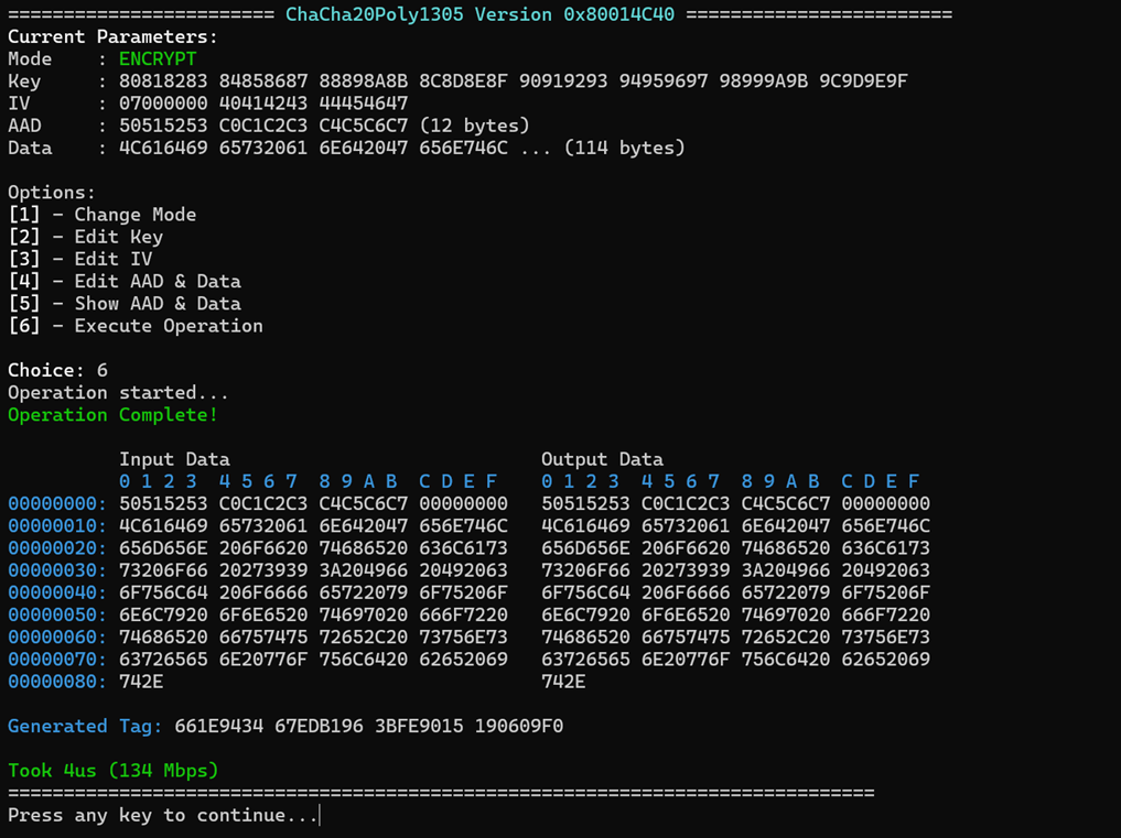
Figure 12 Bypass Mode result
5 Revision History
|
Revision |
Date (D-M-Y) |
Description |
|
1.00 |
30-Jul-26 |
Initial version release |