AAT QDMA using Low Latency IPs Demo
Reference Design Manual
2.1 Network Subsystem (DG LL-IP)
2.1.1 Transceiver (PMA for 10GBASE-R)
2.1.4 LL10GEMACTxIF and LL10GEMACRxIF
3.3.1 Network Driver (DG LL-IP)
3.5.2 demo_setup_with_datamover.cfg
1 Introduction
High-Frequency Trading (HFT) is an advanced form of algorithmic trading where sophisticated computer programs execute a large number of orders at extremely high speeds, often within microseconds. This approach capitalizes on minute price discrepancies in financial markets, aiming to generate profits from rapid, short-term market movements.
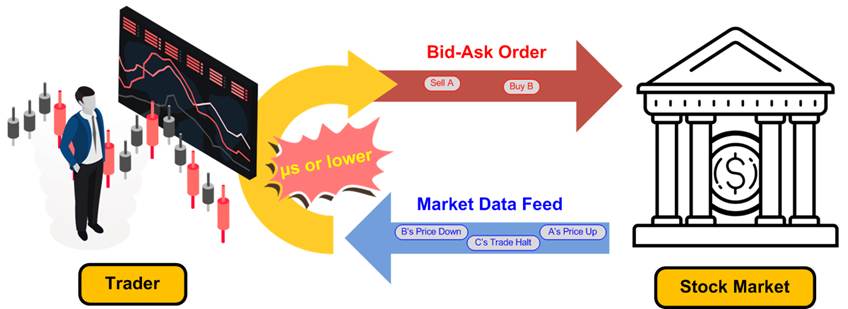
Figure 1 High-Frequency Trading (HFT) Scheme
The competitive landscape of HFT is predominantly defined by latency - the time delay between the initiation of a market event and the corresponding trading response. In this domain, even nanosecond-level advantages can significantly impact profitability. Consequently, HFT firms invest heavily in ultra-low-latency technologies to process market data and execute trades faster than their competitors.
Success in HFT hinges on the ability to swiftly analyze incoming market data and promptly submit bid-ask orders. Traders who can reduce latency in these processes are more likely to secure favorable trade positions, thereby enhancing their potential for substantial profits. This relentless pursuit of speed underscores the critical importance of low-latency systems in the HFT industry.
For maintaining a competitive edge in the trader system, various system architectures have been developed as shown in Figure 2.
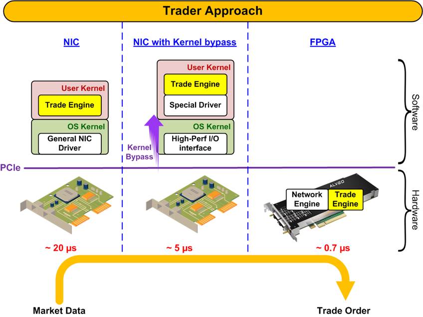
Figure 2 Trader System Approach for HFT
The first solution (most left) is Network Interface Card (NIC) with Software Trading Engine. This conventional approach utilizes a standard NIC to handle network tasks, allowing the CPU to focus on executing the trading algorithms. However, the reliance on the operating system's kernel and networking stack introduces inherent latencies. In HFT environments, this configuration typically results in response times of approximately 20 microseconds or higher.
To reduce more latency, Kernel Bypass concept (middle) is integrated to the first approach (NIC with Software Trading Engine). This method employs specialized NICs capable of bypassing the operating system's kernel, thereby minimizing the overhead associated with kernel-level processing. By leveraging user-space drivers and high-speed I/O interfaces, this architecture can achieve response latencies around 5 microseconds. Implementations often utilize technologies such as Data Plane Development Kit (DPDK) to facilitate kernel bypass and enhance performance.
The most advanced solution integrates the entire trading system within an FPGA (most right), encompassing both network processing and trading logic. By offloading critical tasks to FPGA logic and utilizing on-chip processors for complex algorithms, this architecture achieves minimal latency, often as low as 700 nanoseconds. The hardware-level processing inherent in FPGAs enables rapid data handling and decision-making, providing a significant advantage in time-sensitive trading scenarios.
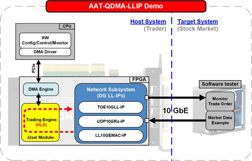
Figure 3 Overview of Accelerated Algorithmic Trading with LL-IPs and QDMA Demo
Building upon the FPGA-based approach mentioned earlier, Design Gateway presents the Accelerated Algorithmic Trading with LL-IPs and QDMA (AAT-QDMA-LLIP) demo, which demonstrates a high-performance trading system over 10G Ethernet. This demonstration consists of two primary components: Host and Target.
The Host serves as the trader's platform and consists of a PC or server equipped with an FPGA card. The entire trading system is implemented within the FPGA, which is designed with three key modules:
· Network Subsystem: Integrates Design Gateway’s complete Low-Latency IP suite, consisting of LL10GEMAC-IP, UDP10GRx-IP, and TOE10GLL-IP, to optimize both the network and transport layers. This configuration significantly reduces latency for UDP-based market data reception and TCP-based order transmission.
· Trading Engine (User Module): Developed using High-Level Synthesis (HLS), this module implements trading algorithms and strategies tailored to specific market protocols, allowing for customization with high-level programming languages.
· DMA Engine: Facilitates efficient communication between the FPGA logic and the Host CPU via PCI Express (PCIe), enabling high-speed data transfer and control.
The Host CPU's role in this demo is primarily confined to configuration, status monitoring, and hardware control through the PCIe interface. The trading algorithm is fully integrated into the FPGA logic to achieve minimal latency. However, for more complex scenarios such as risk management or advanced computations, the Host CPU can process these tasks. In such cases, high-speed data transfer between the FPGA and CPU is critical, facilitated by the DMA engine over PCIe interface. This enables real-time exchange of the order book data and computational results.
The Target acts as a testing platform, simulating the role of a Stock Market. It runs dedicated software that performs two essential functions: sending sample market data to the Host and receiving Bid-Ask orders generated by the FPGA.
This interaction demonstrates a fully functional FPGA-based trading system, showcasing the high-speed order generation and response process.
The AAT-QDMA-LLIP demo delivers notable benefits to trading system developers and traders:
· Reduced development time and faster time-to-market: By providing a complete framework with pre-validated DMA and Ethernet engines, the demo enables traders to focus on developing and customizing the user module within the FPGA. The use of High-Level Synthesis (HLS) simplifies the development process, allowing for algorithm implementation using high-level programming languages and facilitating integration with specific stock market protocols.
· Adaptability and portability: While the AAT-QDMA-LLIP demo is initially demonstrated on AMD Alveo FPGA cards, its development using the Vivado platform ensures portability across various FPGA boards. This flexibility allows traders to seamlessly adapt the system to their preferred hardware platforms.
· Low-Latency performance: By integrating Design Gateway’s Low-Latency IP suite, the AAT-QDMA-LLIP demo delivers a robust FPGA-based trading system capable of achieving the low-latency performance essential for high-frequency trading (HFT) applications.
The subsequent sections provide a detailed description of the Host and Target components, offering further insights into the architecture and capabilities of the AAT-QDMA-LLIP system.
2 Host Hardware
The AAT-QDMA-LLIP framework connects the Host and Target systems through four 10G Ethernet channels. Two channels handle UDP Market Data from the Target, one channel manages TCP Bid-Ask Orders from the Host, and the remaining channel is reserved for loopback testing to measure latency. However, a minimum of two Ethernet channels is required to run the demo—one for UDP Market Data and one for TCP Orders. The Host system is primarily implemented on an FPGA card, while the Target system uses a simple PC running test software that interfaces with the Ethernet network via a standard Network Interface Card (NIC).
This section introduces two hardware configurations: Pricing Engine on Card and Pricing Engine Software. In the first configuration, the entire trading engine is implemented within the FPGA logic, with the Host CPU responsible only for system configuration and parameter control, requiring minimal data transfer. In the second configuration, the FPGA logic acts as an accelerator, working alongside the CPU software. This approach involves significant data transfer between the CPU and FPGA logic to enable real-time processing. Further details for each hardware system are described in the following sections.
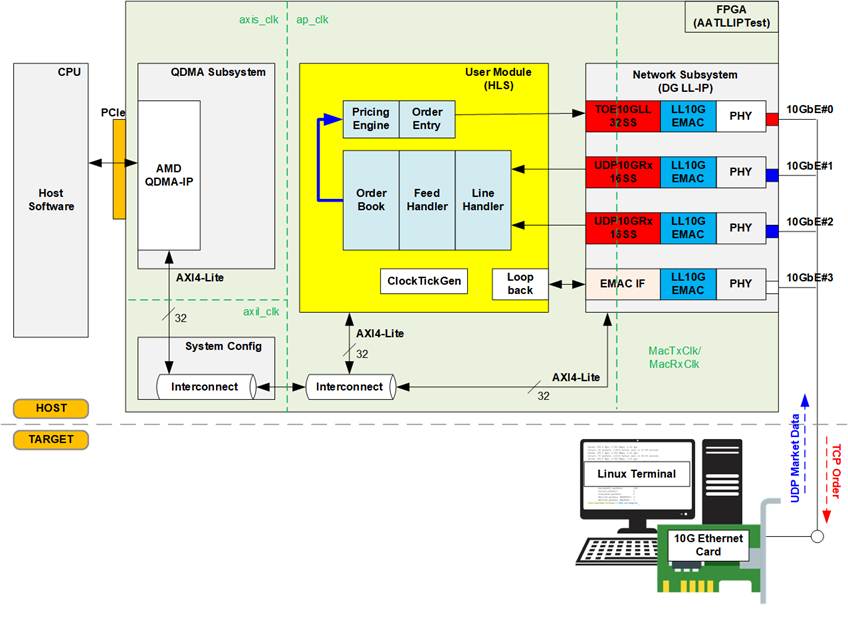
Figure 4 Host Hardware on AAT-QDMA-LLIP Demo (Pricing Engine on Card)
Figure 4 illustrates the Host hardware architecture, which is entirely implemented in FPGA logic. This architecture comprises four main hardware blocks. The first block is the Network Subsystem, responsible for handling transport layer and lower-level protocols across four Ethernet channels. It integrates Design Gateway’s Low-Latency IP suite, including LL10GEMAC-IP, UDP10GRx-IP, and TOE10GLL-IP, to achieve ultra-low latency communication.
The LL10GEMAC, in conjunction with AMD PHY, ensures minimal physical-layer latency, while UDP10GRx16SS and TOE10GLL32SS manage multiple sessions of transport-layer protocols with optimized throughput and response time. Additionally, Design Gateway’s adapter logics manage data-width conversion and clock-domain crossing between the network subsystem and the upper layers.
The second hardware block is the User Module, which is allocated for the user's trading engine. This region is developed entirely using High-Level Synthesis (HLS), ensuring adaptability for different trading markets. AAT-QDMA-LLIP implements this region based on AMD reference designs, incorporating a loopback module and several trading sub-blocks (depicted as blue blocks), such as the Line Handler, Feed Handler, and Order Book.
Communication between the FPGA card and the Host CPU occurs via a PCI Express slot. To facilitate this interaction, the QDMA Subsystem is included in the Host hardware, primarily leveraging AMD's QDMA IP Core. This subsystem is typically used for hardware register access, enabling the Host CPU to control, configure, and monitor the FPGA sub-blocks. Each hardware submodule is equipped with an AXI4-Lite interface for efficient register access.
The final hardware block, System Config, bridges the AXI4-Lite interface between the QDMA-IP and other hardware components. In addition to this role, it manages miscellaneous tasks, e.g., card sensor management, hardware soft-reset control, and etc.
The Host hardware incorporates four distinct clock domains. The first is MacTxClk/MacRxClk, derived from AMD PHY, operating at 322.265625 MHz to support 10G Ethernet functionality. The second is axis_clk, generated by the QDMA-IP, running at a fixed frequency of 250 MHz for the PCIe interface. The third is axil_clk, dedicated to the System Config block for managing Alveo card facilities, operating at 125 MHz. Lastly, the ap_clk domain drives the User Module region and can be adjusted based on the trader's requirements to optimize resource utilization and performance. For the Alveo X3255, the ap_clk frequency is configured to 312.5 MHz.
As the flow shown in Figure 4, once Order Book is updated from the processed market data, the Pricing Engine then uses the updated Order Book and the trading strategy to determine the next trading action, passing this information to the Order Entry. If required, Bid-Ask orders are generated and transmitted as TCP packets. In this configuration, the entire trading engine (highlighted in blue) operates directly on the FPGA card, a structure known as “Pricing Engine on Card”.
In scenarios where trading strategies and algorithms become more complex, FPGA logic alone may not handle all computations efficiently. In such cases, the AAT-QDMA-LLIP offers an alternative configuration called “Pricing Engine Software”, where advanced calculations are performed by the Host software. This configuration is illustrated in Figure 5.
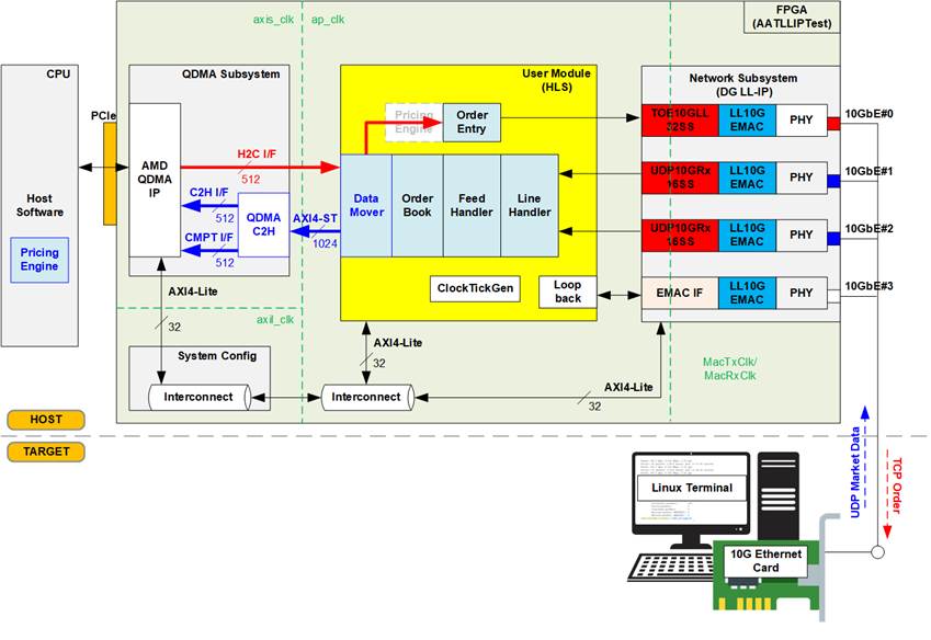
Figure 5 Host Hardware on AAT-QDMA-LLIP Demo (Pricing Engine Software)
In the "Price Engine Software" structure, the Pricing Engine operates within the Host software under the control of the Host CPU. Market data is first processed on the FPGA, and the updated Order Book is transferred to the Host software via a DMA operation. The Data Mover sub-block within the FPGA facilitates this transfer by forwarding the Order Book over a 1024-bit AXI4 stream interface to the QDMA Subsystem. Unlike register access, this data transfer complies with the AMD QDMA IP Core standard. Within this process, the QDMAC2H module reformats the 1024-bit AXI4 stream into 512-bit Controller-to-Host (C2H) and Completion (CMPT) interfaces of the QDMA-IP.
Once the software-based Pricing Engine completes its computations, the results are transferred back to the FPGA trading engine via the Host-to-Controller (H2C) interface. The Data Mover then forwards these results to the Order Entry module, where Bid-Ask orders are generated.
In the AAT-QDMA-LLIP reference design provided by Design Gateway, the Host hardware supports both the "Price Engine on Card" and "Price Engine Software" modes. The primary difference between these configurations lies in the data flow through specific hardware modules:
· In the "Price Engine on Card" mode, the Data Mover and QDMAC2H modules exist within the Host hardware but are inactive as no data flows through them.
· In the "Price Engine Software" mode, the Pricing Engine in the FPGA exists and is implemented, but the data flow bypasses it entirely.
Subsequent sections provide detailed descriptions of each hardware module.
2.1 Network Subsystem (DG LL-IP)
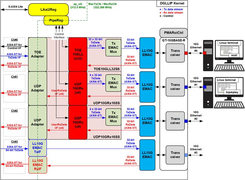
Figure 6 DG LLIP Kernel Block Diagram
The DG LL-IP kernel is integrated into the AAT-QDMA-LLIP system to provide ultra-low-latency Ethernet connectivity. It consists of three key functional modules:
· TCP module (TOE10GLL32SS): Supports up to 32 TCP sessions.
· UDP module (UDP10GRx16SS): Supports up to 16 UDP sessions.
· Loopback module (EMAC): Provides internal testing capability.
Both the TCP and UDP modules require a Control interface for parameter configuration (e.g. MAC address) via LAxi2Reg module. System monitoring is also performed through LAxi2Reg, using an AXI4-Lite bus connection.
The LL-IP kernel provides four Ethernet channels (Ch#0-Ch#3) over four 10G Ethernet connections. Each channel uses an AXI4-Stream (AXI4-ST) interface to transfer control and data streams:
· Ch#0: Mapped to the TCP module, handling order messages from the Order Entry kernel. The channel interface includes AXI4-ST for control/status, Tx data, and Rx data.
· Ch#1 and Ch#2: Mapped to the UDP module, delivering market data to the Line Handler kernel. The channel interface includes AXI4-ST for Rx data only.
· Ch#3: Mapped to the LL10GEMAC-IP for loopback testing. The channel interface includes AXI4-ST for Tx data and Rx data.
To minimize latency, the TOE10GLL-IP (TCP Handler) and UDP10GRx-IP (UDP Handler) modules are directly connected to the LL10GEMAC-IP. All three modules operate in the same local clock domain (MacTxClk / MacRxClk) provided by the AMD PHY transceiver. To support multiple sessions, 32 TOE10GLL-IPs are included within the TOE10GLL32SS block and 16 UDP10GRx-IPs are included within the UDP10GRx16SS block. The TxEMACMux module aggregates packets from multiple TOE10GLL-IPs and UDP10GRx-IPs into a single output stream for the LL10GEMAC-IP.
While the MAC-side modules run in the PHY clock domain, the user-side channels (Ch#0–Ch#3) interface with other kernels using an application clock (ap_clk), which can be configured to meet system requirements. A higher frequency is recommended to achieve lower latency. To bridge these clock domains, adapter logic modules perform Clock domain crossing (CDC), data bus width conversion, and protocol conversion. PipeReg module is used as asynchronous buffer for the control interface, ensuring stable parameter updates to TOE10GLL-IPs and UDP10GRx-IPs.
The LL10GEMAC-IP implements the Ethernet MAC and PCS layers with ultra-low latency and connects directly to the AMD transceiver configured as the PMA module for the 10GBASE-R interface. For reliable operation with low-latency features enabled, the PMARstCtrl module manages the reset sequence of the AMD transceiver.
Further details of each module inside DG LL-IP kernel are described as follows.
2.1.1 Transceiver (PMA for 10GBASE-R)
The PMA IP core for 10Gb Ethernet (BASE-R) can be generated using Vivado IP catalog. In the AMD FPGA Transceivers Wizard, the user uses the following settings.
· Transceiver configuration preset : GT-10GBASE-R
· Encoding/Decoding : Raw
· Transmitter Buffer : Bypass
· Receiver Buffer : Bypass
· User/Internal data width : 32
· Include transceiver COMMON in the : Example Design (not include in Core)
Four channels are enabled in the AAT demo for four Ethernet connections. An example of the Transceiver wizard in Ultrascale model is described in the following link.
https://www.xilinx.com/products/intellectual-property/ultrascale_transceivers_wizard.html.
2.1.2 PMARstCtrl
When bypassing the buffer inside the AMD FPGA transceiver, the user logic must manage the reset signals for both the Tx and Rx buffers. This function is implemented using a state machine that follows the steps outlined below:
1) Assert Tx reset of the transceiver to 1b for one clock cycle.
2) Wait until Tx reset done, output from the transceiver, is asserted to 1b.
3) Finish Tx reset sequence and de-assert Tx reset, user interface output, to allow the user logic to begin Tx operation.
4) Assert Rx reset to the transceiver.
5) Wait until Rx reset done, output from the transceiver, is asserted to 1b.
6) Finish Rx reset sequence and de-assert Rx reset, user interface output, to allow the user logic to begin Rx operation.
2.1.3 DG LL10GEMAC
The IP core by Design Gateway implements low-latency EMAC and PCS logic for 10Gb Ethernet (BASE-R) standard. The user interface is 32-bit AXI4-Stream bus. Please see more details from LL10GEMAC-IP datasheet on our website.
https://dgway.com/products/IP/Lowlatency-IP/dg_ll10gemacip_data_sheet_xilinx_en/
2.1.4 LL10GEMACTxIF and LL10GEMACRxIF
The LL10GEMACTxIF module is an adapter for the transmit path of the LL10GEMAC-IP, while the LL10GEMACRxIF module is an adapter for the receive path. These adapters are integrated into Ethernet channel #3 for the loopback function.
Further details about these adapters can be found in the “LL10GEMAC-IP with AAT-QDMA Demo Reference Design” document:
https://dgway.com/products/IP/Lowlatency-IP/ll10gemac-ip-aat-qdma-refdesign-amd/
2.1.5 UDP10GRx16SS
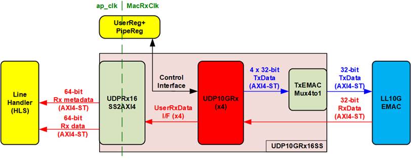
Figure 7 UDP10GRx16SS Block Diagram
To support the reception of multiple market data streams—up to 16 UDP sessions—four UDP10GRx-IPs are integrated for extracting and forwarding packets to the Line Handler. Two adapters, TxEMACMux4to1 and UDPRx16SS2AXI4, manage these connections:
· UDPRx16SS2AXI4: Converts the 32-bit data stream from one of the four UDP10GRx-IPs into a 64-bit data bus for the Line Handler. The session number of the current packet transfer is encoded and forwarded along with the data via the Rx Metadata bus. This module also performs clock domain crossing, converting packet transfers from the MacRxClk domain to the ap_clk domain.
· TxEMACMux4to1: Enables packet transfer from one of the four UDP10GRx-IPs to the LL10GEMAC-IP.
Notes:
1) Further details of the UDPRx16SS2AXI4 and TxEMACMux4to1 modules are provided in Sections 2.6 and 2.4 of the “UDP10GRx-IP 16-Session reference design document”:
https://dgway.com/products/IP/Lowlatency-IP/dg_udp10grx_16ss_refdesign_xilinx_en/
2) Compared with the UDPRx16SS2AXI4 module in the UDP10GRx-IP 16-Session demo, the metadata bus size in the AAT-QDMA-LLIP demo is extended from 16 bits to 64 bits, with the upper additional bits padded with zeros.
· UDP10GRx-IP: Design Gateway IP core that fully offloads UDP/IP packet reception. It connects directly to the Ethernet MAC to extract UDP payload data and deliver it to the user with very low latency. Each core supports up to four UDP sessions. More details are available in the datasheet:
https://dgway.com/products/IP/Lowlatency-IP/dg_udp10grxip_data_sheet_xilinx_en/
Additionally, network parameters such as MAC address and IP address can be defined by the application through the Shell. The UserReg+PipeReg module is used to configure these parameters and to allow the user to read status information from all UDP10GRx-IPs for system monitoring.
2.1.6 TOE10GLL32SS
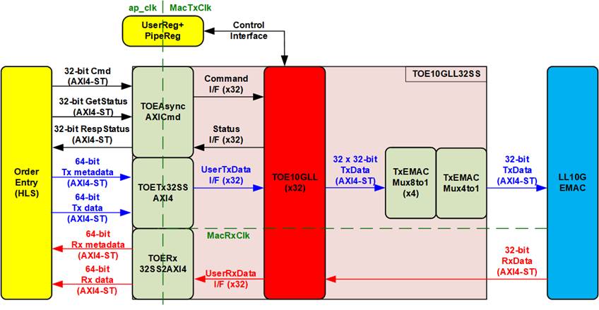
Figure 8 TOE10GLL32SS Block Diagram
For transmitting order packets from the Order Entry via the TCP/IP protocol, TOE10GLL32SS, which contains 32 TOE10GLL-IPs, is used to support up to 32 concurrent TCP sessions. Multiple adapter modules are implemented to interface with these IPs:
· TOEAsyncAXICmd: Interfaces with all TOE10GLL-IPs to generate requests for establishing or terminating TCP sessions and to retrieve command status. It provides three user interfaces: a 32-bit Cmd for connection requests, a 32-bit GetStatus for querying the current status, and a 32-bit RespStatus for retrieving responses from the IPs. This module includes asynchronous logic to transfer signals across clock domains.
· TOETx32SSAXI4: Interfaces with all TOE10GLL-IPs to transmit TCP payload data from the Order Entry to one of the 32 TOE10GLL-IPs. The session number for each payload is defined via the Tx metadata interface. This module also includes an asynchronous buffer for crossing clock domains.
· TOERx32SS2AXI4: Interfaces with all TOE10GLL-IPs to forward received TCP payload data from one of the 32 TOE10GLL-IPs to the Order Entry. The session number of the current payload is transferred via the Rx metadata interface. This module also includes an asynchronous buffer for crossing clock domains.
· TxEMACMux8to1 and TxEMACMux4to1: Implement a 32-to-1 multiplexer to forward transmitted packets from the 32 TOE10GLL-IPs to the LL10GEMAC-IP. Further details are provided in Section 2.5 of “TOE10GLL-IP (Cut-through) 32-Session reference design document”:
https://dgway.com/products/IP/Lowlatency-IP/dg_toe10gllip_32ss_refdesign_xilinx_en/
Additionally, network parameters such as MAC address, IP address, and port number can be defined by the application through the Shell. The UserReg+PipeReg module configures these parameters and allows the user to read status information from all TOE10GLL-IPs for system monitoring.
· TOE10GLL-IP: Implements the TCP/IP stack and offload engine for a low-latency solution. Its user interface has two signal groups: control and data. The IP can operate in two modes: Cut-through mode and Simple mode. The Tx buffer can also be configured to balance resource utilization and test performance. In this reference design, the TOE10GLL-IP is configured in Cut-through mode with an 8 KB Tx buffer. Further details are available in the datasheet:
https://dgway.com/products/IP/Lowlatency-IP/dg_toe10gllip_data_sheet_xilinx_en/
The TOEAsyncAXICmd module connects to three AXI4-ST interfaces. The 32-bit Cmd AXI4-ST, renamed UReqCmd, is used to send three types of commands to one of the 32 TOE10GLL-IPs. The command and target session number are encoded in a 7-bit signal, with 2 bits defining the command type (Active Open, Passive Open, or Active Close) and 5 bits specifying the session number. The 32-bit GetStatus AXI4-ST, renamed UReqSts, is used to request the status of a specific TOE10GLL-IP, where the 5-bit input selects the session number. The 32-bit RespStatus AXI4-ST, renamed URlySts, is used to return the status of the requested TOE10GLL-IP.
· Cmd AXI4-ST I/F (UReqCmd I/F)
The signal UReqCmdData[6:0] encodes both the command and the session number, where bits [4:0] specify the requested session number and bits [6:5] define TCPCmd[1:0] of the TOE10GLL-IP. When a data word is received, one command is issued to the specified TOE10GLL-IP, and before sending a new request, the system must confirm that the targeted TOE10GLL-IP is ready to accept another command.
Figure 9 shows the timing diagram of command generation to the TOE10GLL-IP after a user request is sent to this module.
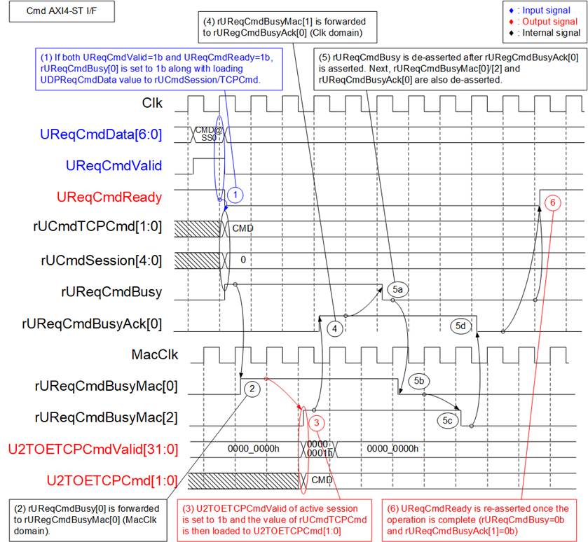
Figure 9 Cmd AXI4-ST I/F Timing Diagram
1) When a new command is requested by the user (UReqCmdValid=1b and UReqCmdReady=1b), the seven lower bits are loaded. Bits[1:0], which hold the command value, are loaded into rUCmdTCPCmd, while bits [6:2], which hold the session number, are loaded into rUCmdSession. At the same time, rUReqCmdBusy is asserted to 1b to start forwarding the command from the Clk domain to the MacClk domain through asynchronous registers. UReqCmdReady is de-asserted to 0b to block any new requests until the operation is complete.
2) rUReqCmdBusy in the Clk domain is forwarded to the MacClk domain using three registers: rReqCmdBusyMac[0]–[2]. All signals are asserted once rUReqCmdBusy is asserted.
3) In Figure 9, the active session is no.0. Therefore, bit 0 of U2TOETCPCmdValid is asserted to 1b along with the command value available on U2TOETCPCmd. The 32 bits of U2TOETCPCmdValid are used to assert the request to all 32 TOE10GLL-IPs. This occurs at the same time as rUReqCmdBusyMac[2] is asserted, which indicates that the command request on the MacClk domain is completely generated.
4) rUReqCmdBusyMac[2] in the MacClk domain is forwarded back to the Clk domain through an asynchronous register, rUReqCmdBusyAck[0].
5) rUReqCmdBusyAck confirms that the command request in the MacClk domain is complete. As a result, rUReqCmdBusy is de-asserted to 0b after rUReqCmdBusyAck[0] is asserted for two clock cycles. Afterward, rUReqCmdBusy is forwarded through the asynchronous register chain in the following sequence:
rUReqCmdBusy -> rUReqCmdBusyMac[0] -> [1] -> [2] -> rUReqCmdBusyAck[0].
At this point, all signals are de-asserted to 0b.
6) Once the operation is complete (rUReqCmdReady=0b and rUReqCmdBusyAck[1]=0b), rUReqCmdReady is re-asserted to 1b to accept the next command request from the user.
· Status AXI4-ST I/F (UReqSts I/F and URlySts I/F)
UReqStsData[4:0] specifies the requested session number for obtaining the latest status. The response is returned on URlyStsData[12:0], which contains the 5-bit session number, a busy flag, a connection ON/OFF flag, an initialization-done flag, and a 5-bit TOE10GLL-IP state. A new request can only be issued after the current status response has been fully returned.
Figure 10 shows the timing diagram of a status request initiated by the user and the corresponding response from the TOE10GLL-IP.
1) When a status request is received (UReqStsValid=1b and UReqStsReady=1b), the session number in UReqStsData[4:0] is loaded into the rUReqStsSSLat signal. The state then changes to stGenReq to begin the operation. At this time, UReqStsReady is de-asserted to 0b to block further requests until the operation is complete. The active session number is also forwarded to the MacClk domain via the asynchronous register (rUReqStsSSMac0).
2) In stGenReq, the request signal (rStsReq) is asserted to 1b to initiate the status request operation. This signal is passed to the MacClk domain using three registers: rStsReqMac[0]–[2].
3) The active session number (rUReqStsSSMac0) selects the corresponding status from one of the 32 TOE10GLL-IPs to be returned on the URlyStsData bus. This selection uses two stages of multiplexers: four 8-to-1 multiplexers and one 4-to-1 multiplexer. In the example shown in Figure 10, the status of TOE10GLL#16 is selected because rUReqStsSSMac0 equals 16. The signal rRlyStsxx2 is valid before rStsReqMac[2] is asserted.
4) The request signal in the MacClk domain (rStsReqMac) is returned to the Clk domain as an acknowledgment signal using two asynchronous registers (rStsReqAck[0]–[1]). This confirms that the request has been successfully asserted in the MacClk domain. The status on rRplyStsxx2 is also returned to the Clk domain via an asynchronous register (URlyStsData).
5) When rStsReqMac[2] is asserted, the state changes to stRlySts. In this state, URlyStsValid is asserted to 1b to indicate that the status is available on URlyStsData. At the same time, rStsReq is de-asserted to 0b to complete the request.
6) If the status is accepted (URlyStsValid=1b and URlyStsReady=1b), the state transitions to stWtDone, and URlyStsValid is de-asserted to 0b.
7) When rStsReq is de-asserted, it propagates through the asynchronous register chain in the following sequence: rStsReqMac[0] -> [1] -> [2] -> rStsReqAck[0] -> [1]. All signals are eventually de-asserted to 0b, clearing the request.
8) After all request signals in the logic are cleared (indicated by the last signal in the update chain, rStsReqAck[1], being de-asserted to 0b), the state returns to stIdle. At this point, UReqStsReady is re-asserted to 1b, allowing a new status request to be accepted.
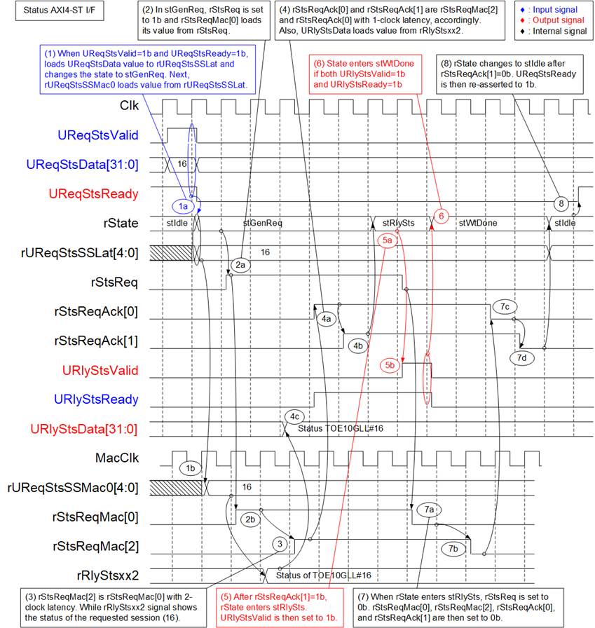
Figure 10 Status AXI4-ST I/F Timing Diagram
The TOETx32SSAXI4 module is an adapter that transmits order messages from the Order Entry kernel to one of the 32 TOE10GLL-IPs. The Order Entry interface consists of a 64-bit UDataTx interface and a 33-bit UMetaDataTx interface, both using the AXI4-ST standard and operating in the Clk domain (system ap_clk). In contrast, the TOE10GLL-IP interface uses a 32-bit data interface, with its parameters decoded from the UMetaDataTx interface in the MacClk domain (system MacTxClk). Therefore, the signals of UDataTx and UMetaDataTx interfaces must be forwarded to the TOE10GLL-IP through an AXI4-ST clock domain crossing, which also performs 64-to-32-bit data width conversion.
This module is designed to achieve low-latency performance, which imposes certain limitations:
· The MacClk-to-Clk frequency ratio must be less than 2.
· If UDataTxValid is de-asserted during transmission and the read logic fails to fetch new data in time, the target TOE10GLL-IP will receive a corrupted packet. According to the TOE10GLL-IP specification, receiving incorrect input requires resetting the connection.
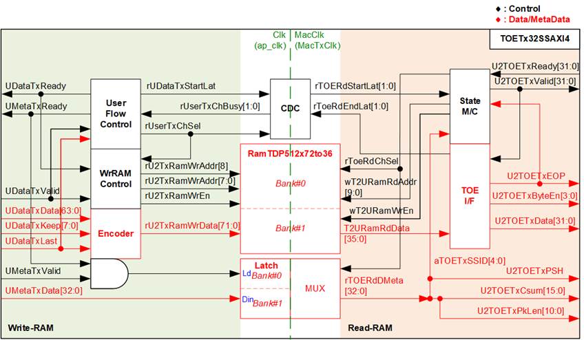
Figure 11 TOETx32SSAXI4 Block Diagram
As shown in Figure 11, a RAMTDP512x72to36 block stores the UDataTx interface, while a latch register stores the UMetaDataTx interface. Both the RAM and the latch are divided into two banks to operate as a double buffer. The left-hand side logic writes to the RAM and latch under Clk, while the right-hand side logic reads them under MacClk. Clock domain crossing (CDC) is implemented to transfer flow control signals across domains, including rUDataTxStartLat (start transfer to TOE) and rTOERdEndLat (transfer to TOE complete).
· RamTDP512x72to36 and Latch
The RamTDP512x72to36 module is a block memory configured as a true dual-port block RAM with asymmetric data width. Data written with 72-bit width in the Clk domain is read out with 36-bit width in the MacClk domain. Each 36-bit word consists of 32-bit data, a 2-bit encoded keep, a 1-bit last flag, and a 1-bit data valid flag. The data valid flag can be written by both the write controller and the read controller: the write controller sets it to 1 when new data is written to RAM, and the read controller clears it to 0 when data is read. This mechanism allows the read controller to detect underflow conditions, which occur if the write controller pauses data transmission for multiple cycles.
The RamTDP512x72to36 is divided into two banks for storing AXI4-Stream data from the user. Bank 0 uses memory addresses 0–255, and Bank 1 uses addresses 256–511. Each bank stores one packet, so the maximum packet length is 2048 bytes (256 × 64 bits). The active bank is switched when the write or read controller completes writing or reading a packet.
Similarly, the latch register is divided into two parts to store metadata for two packets. The 33-bit metadata includes an 11-bit packet size, a 16-bit data checksum, a push flag, and a 5-bit session ID number. The packet size, checksum, and push flag are forwarded to the TOE10GLL-IP when sending the first word of a packet, while the session ID is used to select one of the 32 TOE10GLL-IPs.
· Write-RAM
The User Flow Controller asserts UDataTxReady to accept a new packet transmission when the next RAM bank is free. The address counter increments from 0 to store the first word of each packet. After the final word of a packet is transferred, the MSB of the address is inverted to switch the active bank.
In addition, the User Flow Controller asserts the start-transfer flag (rUDataTxStartLat) when the first word of a new packet and its metadata are received. This signal is forwarded to the state machine (inside the Read-RAM) via CDC to initiate packet transmission to the TOE10GLL-IP. After the state machine transfers the final word of a packet from a bank, the end flag (rTOERdEndLat) is asserted. When the end flag is asserted, the busy flag indicating the RAM status (0 = Free, 1 = Full) is cleared. At this point, the User Flow Controller can use the freed bank to store the next packet.
Figure 12 shows the timing diagram for storing a received packet into RAM.
· Read-RAM
The state machine controls data flow to forward read data from the RAM to the TOE10GLL-IP. The read operation begins when the start flag on MacClk (rTOERdStartLat) is asserted and the active TOE10GLL-IP is ready to receive data (U2TOETxReady=1b). The active TOE10GLL-IP is selected using part of the metadata (aTOETxSSID). To initiate the transfer, U2TOETxValid for the active TOE10GLL-IP is asserted to 1b.
The state machine generates the read address, and the RAM data together with the parameters from the latch are continuously read and forwarded to the TOE10GLL-IP for each packet. If an underflow flag (data valid=0b) is found, it concludes that the last data word has been transferred and asserts the last flag to the TOE10GLL-IP. In this case, the transmitted packet length and checksum will not match the actual data, causing an error in the TOE10GLL-IP.
When the final data word of a packet is transmitted successfully, the state machine switches the RAM bank for the next packet transmission and asserts the end flag (rTOERdEndLat).
Figure 13 shows the timing diagram for forwarding a packet from RAM to the TOE10GLL-IP.
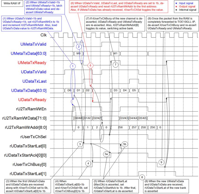
Figure 12 TOETx32SSAXI4 (Write RAM I/F) Timing Diagram
1) When a new data packet is received (UDataTxValid=1b) and the RAM is free to store it (UDataTxReady=1b), the received data (UDataTxData) is written to RAM by asserting rU2TxRamWrEn=1b. The 72-bit write data (rU2TxRamWrData) is formatted into two 36-bit words, each consisting of 32-bit data, a 2-bit encoded byte enable, a last flag, and a data-valid flag. The write RAM address (rU2TxRamWrAddr) increments on bits [7:0], starting from 0, while bit [8] is used as the bank address, loaded from rUserTxChSel.
2) When the metadata containing the packet parameters is received (UMetaTxValid=1b and UMetaTxReady= 1b), it is stored in the latch register of the active channel (e.g., Ch#0 when rUserTxChSel=0). Since each packet has one metadata entry, UMetaTxReady is de-asserted to 0b after the metadata is received to block additional transfers until the logic is ready for the next packet.
3) When both the metadata (UMetaTxData) and the first data word (UDataTxData) are received, the start flag of the active channel is asserted (rUDataTxStartLat[0]=1b when rUserTxChSel=0b).
4) On the next clock cycle after rUDataTxStartLat is asserted, the busy flag of the active channel (rUserTxChBusy) is asserted to 1b, preventing new data from being written to this RAM bank.
5) The start flag in the Clk domain (rUDataTxStartLat) is transferred to the MacClk domain. When the start flag is asserted in the MacClk domain, rUDataTxStartAck is asserted to 1b. Once this acknowledgment is received, rUDataTxStartLat is de-asserted to clear the request for this channel.
6) Data continues to be written to RAM until the final word of the packet is received. When the last word is detected (UDataTxValid=1b and UDataTxLast=1b), UDataTxReady is de-asserted to 0b to block new packets until the logic is prepared. Once both the last data word (UDataTxData) and the corresponding metadata (UMetaTxData) are fully received, the active channel (rUserTxChSel) toggles. At the same time, bits [7:0] of the write RAM address are reset to 0, preparing the new bank to store the next packet from the start address.
7) When the active channel is switched and the new RAM bank is ready (rUserTxChBusy of the new channel = 0b), UMetaTxReady and UDataTxReady are re-asserted to 1b, enabling reception of new metadata and packet data. The new packet is then written into RAM starting at address 0 of the new bank, and its metadata is stored in the latch register of the new channel.
8) Similar to step (3), the start flag of the new channel is asserted (rUDataTxStartLat[1]=1b when rUserTxChSel=1b) to request packet forwarding from the RAM to TOE10GLL-IP.
9) After the packet from RAM has been completely forwarded to the TOE10GLL-IP, the busy flag of the first channel (Ch#0) is de-asserted to 0b, indicating the RAM is free to store a new packet. At this point, UDataTxReady and UMetaTxReady can be asserted to 1b again when the active channel switches back to Ch#0.
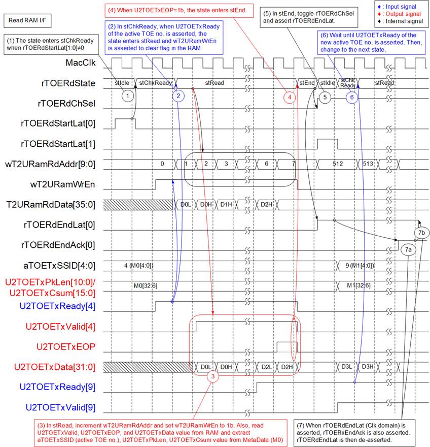
Figure 13 TOETx32SSAXI4 (Read RAM I/F) Timing Diagram
1) The metadata from the latch register is loaded into aTOETxSSID (the active TOE10GLL-IP number), U2TOETxPkLen (packet length), and U2TOETxCsum (TCP checksum). The active channel is controlled by rTOERdChSel. Operation begins when rTOERdStartLat[0] or [1] is asserted in stIdle, after which the state changes to stChkReady.
2) The U2TOETxReady signal of the active TOE10GLL-IP (e.g., Ch#4 when aTOETxSSID=4) is monitored. When it is asserted, the state transitions to stRead. At the same time, wT2URamRdAddr increments to fetch the next data word, and wT2URamWrEn is asserted to clear the RAM entries that have been read.
3) In stRead, RAM data and metadata from the latch register are transferred to the active TOE10GLL-IP. The 36-bit RAM data is split into 32-bit payload (U2TOETxData), a last flag (U2TOETxEOP), and a decoded byte enable (U2TOETxByteEn). The parameters U2TOETxPkLen and U2TOETxCsum are also provided to the TOE10GLL-IP. Data and control flags continue to be forwarded until the final data word is transmitted.
4) When the final data word is forwarded (U2TOETxEOP=1b), U2TOETxValid is de-asserted and the state transitions to stEnd.
5) In stEnd, rTOERdChSel toggles to switch the active channel. wT2URamRdAddr is reset to the start address of the new channel, and rTOERdEndLat is asserted to indicate completion. The state then returns to stIdle.
6) The packet from the new channel is forwarded from RAM to the next TOE10GLL-IP (e.g., Ch#9 when aTOETxSSID=9). First, U2TOETxReady is monitored, then the state progresses through stChkReady and stRead to forward the packet until its final word is transmitted.
7) The end flag (rTOERdEndLat), which indicates operation completion, is transferred to the Clk domain to de-assert the busy flag (rUserTxChBusy). rTOERdEndAck is asserted once the end flag is fully acknowledged in the Clk domain. Afterward, rTOERdEndLat is de-asserted to clear the completion status.
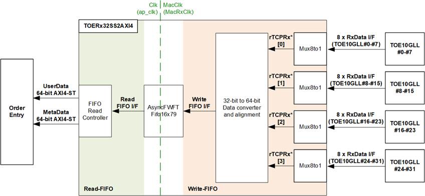
Figure 14 TOERx32SS2AXI4 Block Diagram
Each TOE10GLL-IP supports reception of one TCP session from the EMAC. To handle 32 sessions, 32 TOE10GLL-IPs are instantiated, and their data must be forwarded to the Order Entry for processing. The TOERx32SS2AXI4 adapter transfers the data streams from 32 Rx Data interfaces of TOE10GLL-IPs into two AXI4-ST buses for the Order Entry: a 64-bit UserData bus for TCP payload data and a 64-bit MetaData bus for session numbers. With 32 sessions, only 5 bits of the MetaData bus ([4:0]) are required to encode the session number.
In this design, all TOE10GLL-IPs connect to the same EMAC, so only one session’s data can be transferred at a time. The data stream, synchronous to MacClk, must be converted to the Clk domain, and the session number must be encoded alongside the data. Once 32-bit data and its control signals are completely converted to 79-bit signal (containing 64-bit data, 8-bit byte enable, end-of-packet flag, error flag, and 5-bit session ID), it is stored to an asynchronous FWFT FIFO (AsyncFWFTFifo16x79).
Four Mux8to1 modules are used to reduce input complexity. Each Mux8to1 collects data from eight TOE10GLL-IPs, and its output connects to the data converter and alignment logic. The rTCPRx signal has four indices—[0], [1], [2], and [3]—which correspond to TOE10GLL#0–#7, #8–#15, #16–#23, and #24–#31, respectively.
As shown in Figure 14, the internal logic of TOERx32SS2AXI4 is divided into two groups: Write-FIFO and Read-FIFO. The function of the Write-FIFO logic is illustrated in Figure 15 and Figure 16. Figure 15 presents the timing diagram of the 32-bit to 64-bit data converter with alignment and Mux8to1 writing to the FIFO when the total data received from TOE10GLL-IP#0 is aligned to 64 bits, so no dummy word is required. Figure 16 shows the case where the total received data is not aligned to 64 bits, and one dummy word is inserted.
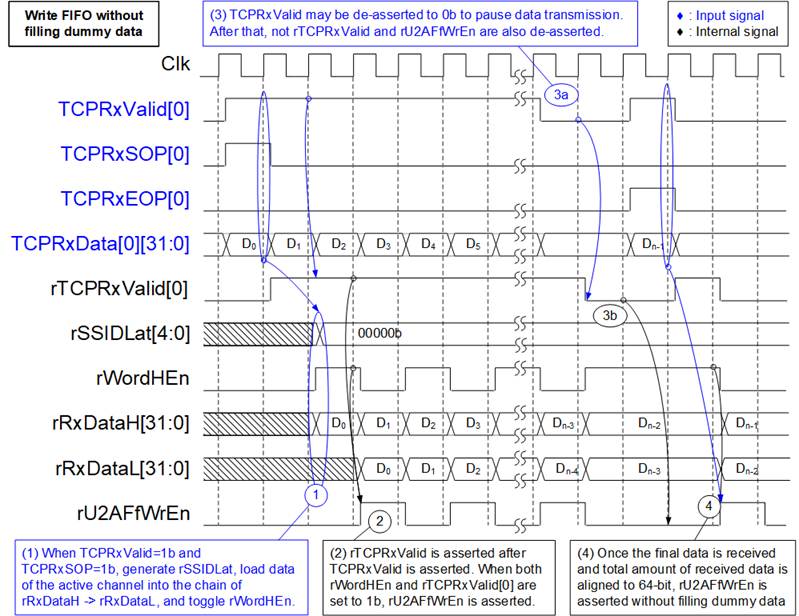
Figure 15 Timing Diagram of Write-FIFO without Filling Dummy Data
1) When a new packet is received from the TOE10GLL-IP (TOERxValid[x]=1b and TOERxSOP[x]=1b), the session ID (rSSIDLat) is decoded from TOERxValid. For example, rSSIDLat=0 when bit 0 of TCPRxValid is asserted. The RxData interface of the active TOE10GLL-IP (TCPRxValid, TCPRxSOP, TCPRxEOP, TCPRxData, TCPRxByteEn, and TCPRxError) is fed to the Mux8to1. The Mux output (rTCPRx* interface) is then forwarded to the data converter and alignment logic. As a result, the latency from TCPRxData to rRxDataH (FIFO input) is two cycles: one cycle from the Mux8to1 and one cycle from the converter and alignment. While TCPRxValid[0] is asserted, rWordHEn is toggled to count the received data in 64-bit units, and rRxDataL loads the value from rRxDataH to form the lower 32 bits of the 64-bit FIFO write data.
2) When two 32-bit words are received (rTCPRxValid[0]=1b and rWordHEn=1b), the 64-bit data (rRxDataH and rRxDataL) is written to the FIFO by asserting the FIFO write enable (rU2AFfWrEn=1b).
3) When the data is not ready, the TOE10GLL-IP de-asserts TCPRxValid=0b to pause transmission. Consequently, the Mux8to1 output and the FIFO write logic also pause operation by setting both rTCPRxValid[0] and rU2AFfWrEn to 0b.
4) When the final data word of a packet is received with 64-bit alignment (rTCPRxValid[0]=1b, rTCPRxEOP[0]=1b, and rWordHEn=1b), the final 64-bit data is written to the FIFO without inserting dummy data for alignment.
Note: rTCPRxValid[0] and rTCPRxEOP[0] are outputs of Mux8to1 which are asserted one clock cycle after TCPRxValid[0] and TCPRxEOP[0] are asserted.
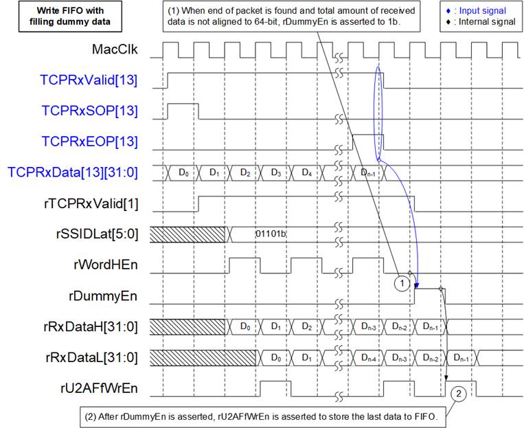
Figure 16 Timing Diagram of Write-FIFO with Filling Dummy Data
1) When the final data of a packet is received and the total amount of data is not aligned to 64 bits (rTCPRxValid[1]=1b, rTCPRxEOP[1]=1b, and rWordHEn=0b), rDummyEn is asserted to 1b to insert one dummy 32-bit word.
Note: rTCPRxValid[1] and rTCPRxEOP[1] are the outputs of Mux8to1. They are asserted one clock cycle after TCPRxValid[13] and TCPRxEOP[13] asserted.
2) After rDummyEn is asserted, rRxDataL loads the last valid data from rRxDataH, while the dummy data is loaded into rRxDataH. Meanwhile, rU2AFfWrEn is asserted to 1b to store the final 64-bit word in the FIFO, consisting of 32 bits of valid data in rRxDataL and 32 bits of dummy data in rRxDataH.
Figure 17 shows the timing diagram of the FIFO-Read, which reads data from the FIFO and forwards it to the Order Entry via the 64-bit UserData AXI4-ST bus. At the same time, the session number is assigned through the 16-bit MetaData AXI4-ST bus. A single MetaData word indicating the session number of the data stream is transferred together with the first UserData word.
The FIFO in this design is the FWFT type, so the read data output (U2AFfRdData) is valid in the same cycle that the read enable (wU2AFfRdAck) is asserted to 1b. Each 79-bit word from the FIFO (U2AFfRdData) is assigned as follows:
· Bit[63:0] : 64-bit data
· Bit[71:64] : 8-bit byte enable
· Bit[72] : Last flag, indicating the end of a packet
· Bit[73] : Error flag of the packet
· Bit[78:74] : 5-bit session ID
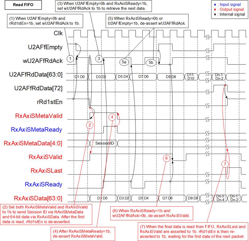
Figure 17 Timing Diagram of FIFO-Read
1) rRd1stEn is asserted to 1b when the read data from the FIFO is the first word of a packet. The FIFO read enable (wU2AFfRdAck) is asserted in two cases:
· If the data is the first word of a packet (rRd1stEn=1b), wU2AFfRdAck is asserted when the FIFO is not empty (U2AFfEmpty=0b).
· If the data is not the first word (rRd1stEn=0b), wU2AFfRdAck is asserted when the FIFO is not empty (U2AFfEmpty=0b) and the user is ready (RxAxiSReady=1b).
Since the FIFO is FWFT type, the read data (U2AFfRdData) is valid in the same cycle that wU2AFfRdAck is asserted.
2) Bits[78:74] of U2AFfRdData are loaded into the metadata output (RxAxiSMetaData), which represents the session ID of the data stream. Metadata is transmitted by asserting the valid signal (RxAxiSMetaValid=1b) when the first word of a packet is read (wU2AFfRdAck=1b and rRd1stEn=1b). Meanwhile, bits[63:0] of U2AFfRdData are loaded into the user data output (RxAxiSData), and the data valid signal is asserted (RxAxiSValid=1b). The data stream remains valid (RxAxiSValid=1b) whenever wU2AFfRdAck=1b. After the first word is read, rRd1stEn is de-asserted to 0b.
3) After the first word, the FIFO read enable (wU2AFfRdAck) is controlled by the FIFO empty flag (U2AFfEmpty) and the user ready signal (RxAxiSReady). It is asserted when U2AFfEmpty=0b and RxAxiSReady=1b. While data is read from the FIFO, U2AFfRdData[63:0] is loaded into RxAxiSData.
4) RxAxiSMetaValid is de-asserted to 0b after the acknowledge signal is asserted (RxAxiSMetaReady=1b).
5) wU2AFfRdAck is de-asserted to 0b to pause reading when the FIFO is empty (U2AFfEmpty=1b) or the user is not ready (RxAxiSReady=0b).
6) If data is sent to the user (RxAxiSValid=1b and RxAxiSReady=1b) but wU2AFfRdAck is de-asserted to 0b, RxAxiSValid is de-asserted to 0b in the next cycle, pausing transmission. It is re-asserted to 1b once wU2AFfRdAck is asserted again, indicating new data is ready.
7) When the final word of a packet is read (U2AFfRdData[72]=1b), the last flag (RxAxiSLast) is asserted to the user. Then, rRd1stEn is re-asserted to 1b to detect the first word of the next packet.
2.1.7 LAxi2Reg
Applications running on the CPU can access hardware through the shell. On AMD platforms, the standard bus for interfacing with hardware registers is AXI4-Lite with a 32-bit data bus. The LL-IP kernel therefore includes the LAxi2Reg module as the interface for writing to and reading from hardware registers. The parameters and status signals of the TOE10GLL32SS, two UDP10GRx16SS modules, and four LL10GEMAC modules are all mapped to LAxi2Reg.
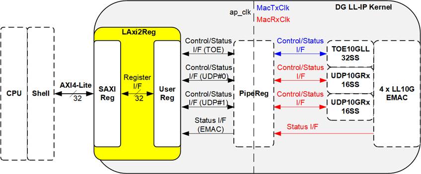
Figure 18 LAxi2Reg Block Diagram
LAxi2Reg consists of SAXIReg and UserReg. SAXIReg converts AXI4-Lite signals into a simplified register interface with a 32-bit data bus (the same width as AXI4-Lite). UserReg contains the register file that stores parameters and status information for the submodules. More details of SAXIReg and UserReg are described below.
This module converts AXI4-Lite signals into a simplified register interface with a 32-bit data bus, matching the AXI4-Lite width. The simplified register interface is compatible with a single-port RAM interface for write transactions. For read transactions, it is slightly modified from the standard RAM interface by adding RdReq and RdValid signals to control read latency. Further details are available in the Section 2.7.1 of the “UDP10GRx-IP 16-Session reference design document”:
https://dgway.com/products/IP/Lowlatency-IP/dg_udp10grx_16ss_refdesign_xilinx_en/
UserReg
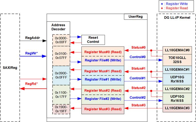
Figure 19 UserReg Block Diagram
The UserReg module consists of multiple registers that interface with the user control interfaces of the TOE10GLL32SS and UDP10GRx16SS modules. The write/read address is decoded by an address decoder to select the active register. Four addressing regions are provided, one for each Ethernet connection. Each region spans 0x800 addresses and is divided into three sections: Reset Control, LL10GEMAC, and TOE10GLL32SS/UDP10GRx16SS. Reset Control is available only in connection #0, while connection #3 contains only LL10GEMAC. Reset Control provides the main reset signal for the DG LL-IP kernel.
As shown in Figure 19, the address space is divided as follows:
1. 0x0000 – 0x07FF : Reset controller and hardware of Ethernet #0
· 0x0000 – 0x00FF : Kernel reset
· 0x0100 – 0x01FF : LL10GEMAC-IP
· 0x0200 – 0x07FF : TOE10GLL32SS)
2. 0x0800 – 0x0FFF : Hardware of Ethernet #1
· 0x0900 – 0x09FF : LL10GEMAC-IP
· 0x0A00 – 0x0CFF : UDP10GRx16SS
3. 0x1000 – 0x17FF : Hardware of Ethernet #2
· 0x1100 – 0x11FF : LL10GEMAC-IP
· 0x1200 – 0x14FF : UDP10GRx16SS
4. 0x1800 – 0x1FFF : Hardware of Ethernet #3
· 0x1900 – 0x19FF : LL10GEMAC-IP
The Address Decoder uses the upper bits of RegAddr to select the active address area, while the lower bits are used to select the active register within that area. The register file inside UserReg has a 32-bit data width, so the write byte enable signal (RegWrByteEn) is not used. To write to hardware registers, the CPU must therefore use a 32-bit pointer. Since UserReg contains many status registers, multi-level multiplexers are used to return the read values during read access. The total read latency is five clock cycles, so RegRdValid is generated from RegRdReq through a chain of five D Flip-Flops. More details of the address mapping within the UserReg module are provided in Table 1.
Table 1 Register Map Definition
|
Wr/Rd |
Register Name (Label in the dg_llnetwork_address_map.h”) |
|
Description |
|
|
BA+0x0000 – BA+0x00FF: Kernel control (Write/Read access) |
|
|
BA+0x0000 |
Kernel reset (DG_LLNETWORK_KERNEL_RESET_CONTROL_OFFSET) |
|
[0]: Mapped to kernel reset (1b-Reset, 0b-Clear). |
|
|
BA+0x0100 – BA+0x01FF: LL10GEMAC-IP#0 (Read access only) Note: The number after Register name is channel number (Ch#0). |
|
|
IP Version of LLEMAC10G-IP DG_LLNETWORK_EMAC_IPVERSION_OFFSET(0) |
|
|
[31:0]: Mapped to IPVersion of LL10GEMAC-IP |
|
|
BA+0x0104 |
Tx Test pin of LLEMAC10G-IP DG_LLNETWORK_EMAC_TXTESTPIN_OFFSET(0) |
|
[7:0]: Mapped to TxTestPin of LL10GEMAC-IP |
|
|
BA+0x0108 |
Rx Test pin of LLEMAC10G-IP DG_LLNETWORK_EMAC_RXTESTPIN_OFFSET(0) |
|
[7:0]: Mapped to RxTestPin of LL10GEMAC-IP |
|
|
BA+0x010C |
EMAC Linkup Status DG_LLNETWORK_EMAC_LINKUP_OFFSET(0) |
|
[0]: Mapped to Linkup of LL10GEMAC-IP (0b-Link down, 1b-Link up) |
|
|
BA+0x0200 – BA+0x07FF: TOE10GLL-IP (Write/Read access) Note: The number after Register name is channel number (Ch#0) |
|
|
BA+0x0200 |
IP Version of TOE10GLL-IP DG_LLNETWORK_TOE_IPVERSION_OFFSET(0) |
|
[31:0]: Mapped to IPVersion of TOE10GLL-IP |
|
|
BA+0x0204 |
Reset of TOE10GLL-IP DG_LLNETWORK_TOE_RESET_OFFSET(0) |
|
[0]: Reset of TOE10GLL#0, [1]: Reset of TOE10GLL#1, …, [31]: Reset of TOE10GLL#31 |
|
|
BA+0x0208 |
Source MAC address (Low) of TOE10GLL-IPs DG_LLNETWORK_TOE_SOURCE_MAC_ADDRESS_LOWER_OFFSET(0) |
|
[31:0]: Mapped to SrcMacAddr[31:0] of all TOE10GLL-IPs |
|
|
BA+0x020C |
Source MAC address (High) of TOE10GLL-IP DG_LLNETWORK_TOE_SOURCE_MAC_ADDRESS_UPPER_OFFSET(0) |
|
[15:0]: Mapped to SrcMacAddr[47:32] of all TOE10GLL-IPs |
|
|
BA+0x0210 |
Source IP address of TOE10GLL-IP DG_LLNETWORK_TOE_SOURCE_IP_ADDRESS_OFFSET(0) |
|
[31:0]: Mapped to SrcIPAddr[31:0] of all TOE10GLL-IPs |
|
|
BA+0x0214 |
Time out of TOE10GLL-IP DG_LLNETWORK_TOE_TIMEOUT_SET_OFFSET(0) |
|
[31:0]: Mapped to TimeOutSet[31:0] of all TOE10GLL-IPs |
|
|
Address Wr/Rd |
Register Name (Label in the dg_llnetwork_address_map.h”) |
|
Description |
|
|
BA+0x0200 – BA+0x07FF: TOE10GLL-IP (Write/Read access) Note: The number after Register name is channel number (Ch#0) |
|
|
Operation mode of TOE10GLL-IP#0 DG_LLNETWORK_TOE_OPMODE_OFFSET(0, 0) |
|
|
[1:0]: Mapped to DstMacMode of TOE10GLL-IP#0 [2]: Mapped to ARPICMPEn of TOE10GLL-IP#0 |
|
|
BA+0x0304- BA+0x037F |
Operation mode of TOE10GLL-IP#1- #31 Similar to 0x0300, define the number of parameters to be (0, 1) – (0,31) instead of (0, 0) |
|
BA+0x0380 |
Transmitted length counter of TOE10GLL#0 DG_LLNETWORK_TOE_COMPLETION_LENGTH_OFFSET (0,0) |
|
[31:0]: Mapped to TCPTxCplLen counter of TOE10GLL-IP#0 |
|
|
BA+0x0384- BA+0x03FF |
Transmitted length counter of TOE10GLL-IP#1-31 Similar to 0x0380, define the number of parameters to be (0, 1) – (0,31) instead of (0, 0) |
|
BA+0x0400 – BA+0x041F: Session#0, BA+0x0420 – BA+0x043F: Session#1, BA+0x0440 – BA+0x045F: Session#2, …, BA+0x07E0 – BA+0x07FF: Session#31 Note: The number after channel number (Ch#0) is session number (SS#0-SS#31). |
|
|
BA+0x0400 |
Destination MAC address (Low) of TOE10GLL-IP#0 DG_LLNETWORK_TOE_DESTINATION_MAC_ADDRESS_LOWER_OFFSET(0, 0) |
|
[31:0]: Mapped to DstMacAddr[31:0] of TOE10GLL-IP#0 |
|
|
BA+0x0404 |
Destination MAC address (High) of TOE10GLL-IP#0 DG_LLNETWORK_TOE_DESTINATION_MAC_ADDRESS_UPPER_OFFSET(0, 0) |
|
[15:0]: Mapped to DstMacAddr[47:32] of TOE10GLL-IP#0 |
|
|
BA+0x0408 |
Destination IP Address of TOE10GLL-IP#0 DG_LLNETWORK_TOE_DESTINATION_IP_ADDRESS_OFFSET(0, 0) |
|
[31:0]: Mapped to DstIPAddr[31:0] of TOE10GLL-IP#0 |
|
|
BA+0x040C |
Source Port Number of TOE10GLL-IP#0 DG_LLNETWORK_TOE_SOURCE_PORT_NUMBER_OFFSET(0, 0) |
|
[15:0]: Mapped to TCPSrcPort [15:0] of TOE10GLL-IP#0 |
|
|
BA+0x0410 |
Destination Port Number of TOE10GLL-IP#0 DG_LLNETWORK_TOE_DESTINATION_PORT_NUMBER_OFFSET(0, 0) |
|
[15:0]: Mapped to TCPDstPort [15:0] of TOE10GLL-IP#0 |
|
|
BA+0x0414 |
Destination MAC address output (Low) of TOE10GLLIP#0 (Read only) DG_LLNETWORK_TOE_DESTINATION_MAC_ADDRESS_OUT_LOWER_OFFSET(0, 0) |
|
[31:0]: Mapped to DstMacAddrOut[31:0] of TOE10GLL-IP#0 |
|
|
BA+0x0418 |
Destination MAC address output (High) of TOE10GLLIP#0 (Read only) DG_LLNETWORK_TOE_DESTINATION_MAC_ADDRESS_OUT_UPPER_OFFSET(0, 0) |
|
[15:0]: Mapped to DstMacAddrOut[47:32] of TOE10GLL-IP#0 |
|
|
BA+0x041C |
IP status of TOE10GLL-IP#0 DG_LLNETWORK_TOE_STATUS_OFFSET(0, 0) |
|
[0]: Mapped to InitFinish of TOE10GLL-IP#0 [1]: Mapped to TCPConnOn of TOE10GLL-IP#0 [20:16]: Mapped to IPState of TOE10GLL-IP#0 |
|
|
Address Wr/Rd |
Register Name (Label in the dg_llnetwork_address_map.h”) |
|
Description |
|
|
BA+0x0200 – BA+0x07FF: TOE10GLL-IP (Write/Read access) Note: The number after Register name is channel number (Ch#0) |
|
|
BA+0x420- BA+0x43F |
Session#1 parameters 0x0420: DG_LLNETWORK_TOE_DESTINATION_MAC_ADDRESS_LOWER_OFFSET(0, 1) 0x0424: DG_LLNETWORK_TOE_DESTINATION_MAC_ADDRESS_LOWER_OFFSET(0, 1) 0x0428: DG_LLNETWORK_TOE_DESTINATION_IP_ADDRESS_OFFSET(0, 1) 0x042C: DG_LLNETWORK_TOE_SOURCE_PORT_NUMBER_OFFSET(0, 1) 0x0430: DG_LLNETWORK_TOE_DESTINATION_PORT_NUMBER_OFFSET (0, 1) 0x0434: DG_LLNETWORK_TOE_DESTINATION_MAC_ADDRESS_OUT_LOWER_OFFSET(0, 1) 0x0438: DG_LLNETWORK_TOE_DESTINATION_MAC_ADDRESS_OUT_UPPER_OFFSET(0, 1) 0x043C: DG_LLNETWORK_TOE_STATUS_OFFSET(0, 1) |
|
BA+0x0440- BA+0x07FF |
Session#2 – Session#31 parameters 0x0440-0x045F: Similar to 0x0400 – 0x041F, define the number of parameters to be (0, 2) 0x0460-0x047F: Similar to 0x0400 – 0x041F, define the number of parameters to be (0, 3). … 0x07E0-0x07FF: Similar to 0x0400 – 0x041F, define the number of parameters to be (0, 31). |
|
BA+0x0900 – BA+0x09FF:LL10GEMAC-IP#1 (Read access only) BA+0x0A00 – BA+0x0CFF: UDP10GRx-IP#1 (Write/Read access) Note: The number after Register name is channel number (Ch#1) |
|
|
BA+0x0900 - BA+0x09FF |
LL10GEMAC-IP#1 Similar to 0x0100 – 0x01FF, define channel number to be (1) |
|
BA+0x0A00 |
IP Version of UDP10GRx-IP (Read only) DG_LLNETWORK_UDP_IPVERSION_OFFSET(1) |
|
[31:0]: Mapped to IPVersion of UDP10GRx-IP |
|
|
BA+0x0A10 – BA+0x0A1F |
Test pin of four UDP10GRx-IPs (Read only) DG_LLNETWORK_UDP_TESTPIN_OFFSET(1,0) – (1,3) Note: The number after channel number (Ch#1) is the UDP10GRx-IP number. There are four UDP10GRx-IPs inside UDP10GRx16SS. |
|
0xA10 [31:0]: Mapped to TestPin of UDP10GRx-IP#0 0xA14 [31:0]: Mapped to TestPin of UDP10GRx-IP#1 0xA18 [31:0]: Mapped to TestPin of UDP10GRx-IP#2 0xA1C [31:0]: Mapped to TestPin of UDP10GRx-IP#3 |
|
|
BA+0x0A20 |
Session Enable Reg DG_LLNETWORK_UDP_SESSION_ENABLE_ACTIVE_OFFSET(1) |
|
Wr - Input to be UDPSSEnable (Session enable) of UDP10GRx16SS [3:0]: Input to SSEnable of UDP10GRx-IP#0 (The enable of Session#0 - #3). [7:4]: Input to SSEnable of UDP10GRx-IP#1 (The enable of Session#4 - #7). [11:8]: Input to SSEnable of UDP10GRx-IP#2 (The enable of Session#8 - #11). [15:0]: Input to SSEnable of UDP10GRx-IP#3 (The enable of Session#12 - #15). Rd – Mapped to UDPSSActive (Sessions active status) of UDP10GRx16SS [3:0]: Mapped to SSActive of UDP10GRx-IP#0 (The active status of Session#0 - #3). [7:4]: Mapped to SSActive of UDP10GRx-IP#1 (The active status of Session#4 - #7). [11:8]: Mapped to SSActive of UDP10GRx-IP#2 (The active status of Session#8 - #11). [15:0]: Mapped to SSActive of UDP10GRx-IP#3 (The active status of Session#12 - #15). |
|
|
Address Wr/Rd |
Register Name (Label in the dg_llnetwork_address_map.h”) |
|
Description |
|
|
BA+0x0A00 – BA+0x0CFF UDP10GRx-IP#1 (Write/Read access) Note: The number after Register name is channel number (Ch#1) |
|
|
Multicast Enable Reg DG_LLNETWORK_UDP_MULTICAST_MODE_OFFSET(1) |
|
|
Wr/Rd [0]: UDPMcastEn (Multicast mode) of UDP10GRx16SS (‘0’-Unicast, ‘1’-Multicast) |
|
|
BA+0x0A40
|
Source MAC address (Low) Reg DG_LLNETWORK_UDP_SOURCE_MAC_ADDRESS_LOWER_OFFSET(1) |
|
Wr/Rd [31:0]: UDPSrcMacAddr[31:0] (Source MAC address) of UDP10GRx16SS |
|
|
BA+0x0A44
|
Source MAC address (High) Reg DG_LLNETWORK_UDP_SOURCE_MAC_ADDRESS_UPPER_OFFSET(1) |
|
Wr/Rd [15:0]: UDPSrcMacAddr[47:32] (Source MAC address) of UDP10GRx16SS |
|
|
BA+0x0A48
|
Source IP address Reg DG_LLNETWORK_UDP_SOURCE_IP_ADDRESS_OFFSET(1) |
|
Wr/Rd [31:0]: UDPSrcIPAddr[31:0] (Source IP address) of UDP10GRx16SS |
|
|
BA+0x0C00 – BA+0x0C3F: Session#0 - Session#3, BA+0x0C40 – BA+0x0C7F: Session#4 – Session#7, BA+0x0C80 – BA+0x0CBF: Session#8 - Session#11, BA+0x0CC0 – BA+0x0CFF: Session#12 – Session#15 Note: The number after channel number (Ch#1) is session number (SS#0-SS#15). |
|
|
BA+0x0C00 |
Source port number Reg DG_LLNETWORK_UDP_SOURCE_PORT_NUMBER_OFFSET(1, 0) |
|
Wr/Rd [15:0]: UDPSrcPort(0) (Source port of Session#0) of UDP10GRx16SS |
|
|
BA+0x0C04 |
Destination port number Reg DG_LLNETWORK_UDP_DESTINATION_PORT_NUMBER_OFFSET(1, 0) |
|
Wr/Rd [15:0]: UDPDstPort(0) (Destination port of Session#0) of UDP10GRx16SS |
|
|
BA+0x0C08 |
Destination IP address Reg DG_LLNETWORK_UDP_DESTINATION_IP_ADDRESS_OFFSET(1, 0) |
|
Wr/Rd [31:0]: UDPDstIPAddr(0) (Destination IP address of Session#0) of UDP10GRx16SS |
|
|
BA+0x0C0C |
Multicast IP address Reg DG_LLNETWORK_UDP_MULTICAST_IP_ADDRESS_OFFSET(1, 0) |
|
Wr/Rd [31:0]: UDPMcastIPAddr(0) (Multicast IP address of Session#0) of UDP10GRx16SS |
|
|
BA+0x0C10 – BA+0x0C1F |
Session#1 parameters 0x0C10: DG_LLNETWORK_UDP_SOURCE_PORT_NUMBER_OFFSET(1, 1) 0x0C14: DG_LLNETWORK_UDP_DESTINATION_PORT_NUMBER_OFFSET(1, 1) 0x0C18: DG_LLNETWORK_UDP_DESTINATION_IP_ADDRESS_OFFSET(1, 1) 0x0C1C: DG_LLNETWORK_UDP_MULTICAST_IP_ADDRESS_OFFSET(1, 1) |
|
BA+0x0C20 – BA+0x0C2F |
Session#2 parameters 0x0C20: DG_LLNETWORK_UDP_SOURCE_PORT_NUMBER_OFFSET(1, 2) 0x0C24: DG_LLNETWORK_UDP_DESTINATION_PORT_NUMBER_OFFSET(1, 2) 0x0C28: DG_LLNETWORK_UDP_DESTINATION_IP_ADDRESS_OFFSET(1, 2) 0x0C2C: DG_LLNETWORK_UDP_MULTICAST_IP_ADDRESS_OFFSET(1, 2) |
|
BA+0x0C30 – BA+0x0C3F |
Session#3 parameters 0x0C30: DG_LLNETWORK_UDP_SOURCE_PORT_NUMBER_OFFSET(1, 3) 0x0C34: DG_LLNETWORK_UDP_DESTINATION_PORT_NUMBER_OFFSET(1, 3) 0x0C38: DG_LLNETWORK_UDP_DESTINATION_IP_ADDRESS_OFFSET(1, 3) 0x0C3C: DG_LLNETWORK_UDP_MULTICAST_IP_ADDRESS_OFFSET(1, 3) |
|
BA+0x0C40 – BA+0x0C7F |
Session#4 – Session#7 parameters Similar to 0x0C00 – 0x0C3F, define the number of parameters to be (1, 4) – (1,7) instead of (1,0) – (1,3). |
|
BA+0x0C80 – BA+0x0CBF |
Session#8 – Session#11 parameters Similar to 0x0C00 – 0x0C3F, define the number of parameters to be (1, 8) – (1,11) instead of (1,0) – (1,3) |
|
BA+0x0CC0 – BA+0x0CFF |
Session#12 – Session#15 parameters Similar to 0x0C00 – 0x0C3F, define the number of parameters to be (1, 12) – (1,15) instead of (1,0) – (1,3) |
|
Address Wr/Rd |
Register Name (Label in the dg_llnetwork_address_map.h”) |
|
Description |
|
|
BA+0x1100 – BA+0x11FF:LL10GEMAC-IP#2 (Read access only) BA+0x1200 – BA+0x14FF: UDP10GRx-IP#2 (Write/Read access) Note: The number after Register name is channel number (Ch#2) |
|
|
BA+0x1100 – BA+0x11FF |
LL10GEMAC-IP#2 Similar to 0x0100 – 0x010F, define channel number to be (2) |
|
BA+0x1200 – BA+0x14FF |
UDP10GRx-IP#2 Similar to 0x0A00 – 0x0CFF, define channel number to be (2) |
|
BA+0x1900 – BA+0x19FF: LL10GEMAC-IP#3 (Read access only) Note: The number after Register name is channel number (Ch#3) |
|
|
BA+0x1900 – BA+0x19FF |
LL10GEMAC-IP#3 Similar to 0x0100 – 0x010F, define channel number to be (3) |
2.2 User Module
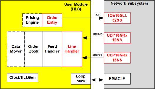
Figure 20 User Module Component
The User Module consists of various submodules developed using High-Level Synthesis (HLS) to minimize development time. These submodules are derived from the AMD Accelerated Algorithmic Trading Demo. However, the DataMover submodule has been specifically modified to interface with the AMD QDMA-IP instead of XDMA-IP, ensuring compatibility with the system’s PCIe data transfer infrastructure.
Market data is generally transmitted over two Ethernet channels using UDP/IP protocols. Duplicated market data on both channels is processed by Line Handler, which merged the data into a single stream. This merged stream is then decoded by the Feed Handler and subsequent submodules, which follow the CME MDP 3.0 Market Data Protocol. This protocol uses the Financial Information Exchange (FIX) format with Simple Binary Encoding (SBE).
By leveraging HLS, users can easily develop, replace, and modify submodules to support specific trading strategies and market requirements. The submodules inside the User Module of the AAT-QDMA-LLIP system are nearly identical to those in the AAT-QDMA system. However, to achieve lower latency, the AAT-QDMA-LLIP replaces the AMD TCP-IP and AMD UDP-IP modules with TOE10GLL32SS and UDP10GRx16SS. Because these IPs use different interfaces than the AMD IPs, the LineHandler and OrderEntry submodules have also been modified to support connectivity with TOE10GLL32SS and UDP10GRx16SS. Further details of the LineHandler and OrderEntry submodules are described in the following sections.
Details of the remaining submodules, which are unchanged from the AAT-QDMA system, can be found in Section 2.2 of the “LL10GEMAC-IP with AAT-QDMA Demo Reference Design” document:
https://dgway.com/products/IP/Lowlatency-IP/ll10gemac-ip-aat-qdma-refdesign-amd/
2.2.1 LineHandler
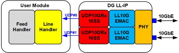
Figure 21 LineHandler Interface
The LineHandler submodule is designed to arbitrate between two UDP streams, referred to as the A Line and B line which are linked to UDP#0 and UDP#1, to ensure reliable data delivery. Many stock exchanges deliver data feeds via UDP multicast, a high-speed but unreliable method where packets can be lost or delivered out of order. By subscribing to two identical multicast streams, the LineHandler ensures data integrity through line arbitration.
The LineHandler uses sequence number embedded in the packet headers to track and process incoming packets. This module outputs a single, reliable stream of market data for subsequent processing by the Feed Handler submodule.
The LineHandler has been modified from the original AMD implementation to support two UDP10GRx16SS modules, with the following changes:
1) The metadata width has been reduced from 256 bits to 64 bits, while the number of module interfaces remains unchanged for ease of system integration. The unused interface can be removed inside the DG LL-IP while maintaining compatibility with the default design.
2) Because the UDP10GRx16SS discards packets with unmatched network parameters, the filtering function inside the LineHandler has been removed.
3) The LineHandler now decodes the Split ID using the metadata signal transmitted by the UDP10GRx16SS module, which provides the UDP session ID (ranging from 0 to 15).
Accordingly, the original AMD LineHandler has been updated as follows:
· In the LineHandler header file, the definitions of IP address and port number are replaced with the session ID.
· In the portFilter function of the linehandler_top C++ source file, the network parameter filter is replaced with a session ID filter.
2.2.2 OrderEntry
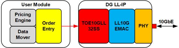
Figure 22 OrderEntry Interface
The OrderEntry submodule processes order placement requests received from the PricingEngine submodule or DataMover submodule. It constructs order messages in the appropriate FIX4.2 protocol format, which includes tags for price, quantity, order ID, and active type.
After constructing the order message, the OrderEntry submodule calculates and appends a partial checksum. The resulting message is passed to the TCP submodule, which completes the encapsulation with IP and TCP headers before transmitting it over the Ethernet interface.
The OrderEntry has been modified from the original AMD implementation to connect with TOE10GLL32SS, with the following changes:
1) Update the interfaces between the OrderEntry and the TCP engine submodules from eight interfaces to be three: connectionCommandStream, requestStatusStream, and connectionStatusStream.
2) Remove the notificationHandlerTcp function due to changes in TCP engine control.
3) Update the connection specification to use the session ID instead of the IP address and port number.
4) Modify the connection and disconnection sequence in the serverProcessTcp function as follows:
i) When a new command is received via the AXI4-Lite interface, OrderEntry sends a request status to TOE10GLL32SS via the requestStatusStream interface to check if the TOE10GLL-IP is ready.
ii) Wait for a response from TOE10GLL32SS via the connectionStatusStream interface. If the TOE10GLL-IP is ready, OrderEntry generates a command request to open or close the connection via the connectionCommandStream interface. Otherwise, return to step (i) and retry until the TOE10GLL-IP is ready.
iii) Generate a request status command to verify whether the requested TOE10GLL-IP has completed the open/close operation.
iv) Decode the response from TOE10GLL32SS. If the response indicates the operation is incomplete, return to step (iii).
2.3 QDMA Subsystem
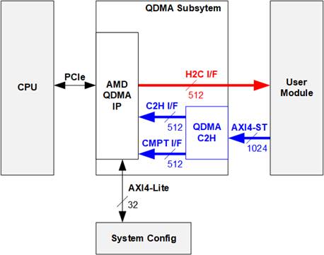
Figure 23 QDMA Subsystem Component
The QDMA subsystem facilitates high-throughput and low-latency data transfer between the FPGA and the Host system via PCIe. It integrates the AMD QDMA IP and QDMA C2H submodule, ensuring compatibility with the trading system’s AXI4 Stream interfaces.
The AMD QDMA IP supports advanced features such as queue-based abstractions, which optimize the handling of small packets in dynamic trading environments. The QDMA C2H submodule adapts the trading system’s data interface to the AMD QDMA IP interface, enabling efficient data flow between the hardware and the host.
This subsystem is identical to the one used in the AAT-QDMA demo. Further details can be found in Section 2.3 of the “LL10GEMAC-IP with AAT-QDMA Demo Reference Design” document.
2.4 System Config
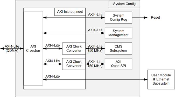
Figure 24 System Config Block Diagram
The System Config module manages system configuration signals using the AXI4-Lite bus interface, which is optimized for single transfers and is not performance-sensitive. Consequently, this module operates on axil_clk, running at a lower frequency than axis_clk and ap_clk. The module comprises several components, including the AXI-Interconnect, System Config Reg, System Management, CMS Subsystem, and AXI Quad SPI.
This subsystem is identical to the one used in the AAT-QDMA demo. Further details are provided in Section 2.4 of the “LL10GEMAC-IP with AAT-QDMA Demo Reference Design” document.
3 Host Software
In the AAT-QDMA-LLIP demo, Host software is divided into two main regions – DPDK and AAT-QDMA-LLIP application as illustrated in Figure 25.
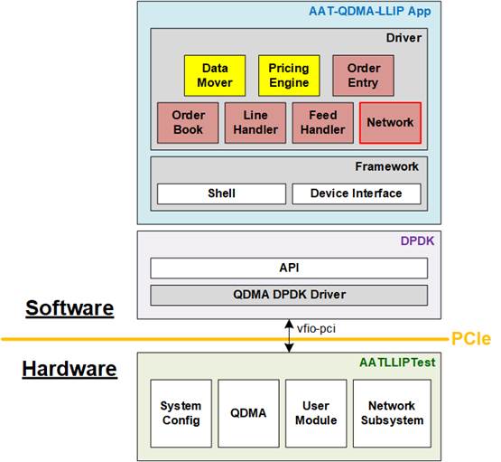
Figure 25 Host Software Structure on AAT-QDMA-LLIP Demo
To enable seamless communication between hardware and software, the Data Plane Development Kit (DPDK) is employed. Using DPDK, the FPGA card (hardware) is directly accessible from the software, bypassing the traditional OS kernel procedures via high-performance I/O virtualization (vfio-pci). In this reference design, DPDK is tailored to work with the AMD QDMA IP Core on the FPGA. As a result, the QDMA DPDK driver is utilized to fulfill the Direct Memory Access (DMA) requirements. DPDK also provides an API that acts as an interface for its driver, offering a set of predefined functions or commands that allow the upper-layer software (AAT-QDMA-LLIP application) to leverage DPDK's capabilities.
Built on top of DPDK, the AAT-QDMA-LLIP application is responsible for managing the demo’s initialization, configuration, hardware register access, and monitoring. This application operates through two key sub-blocks. The first is the Framework, which comprises a set of shared software functions typically used by other software components. The Framework includes functions for interfacing with the user terminal (Shell) and functions for interacting with DPDK for DMA operations and hardware access (Device Interface).
The second sub-block is the Driver, which serves as the interface for controlling each hardware submodule within the FPGA. When managing hardware submodules, the Driver initiates register access to configure or clear specific hardware ports. For data transfer, the Driver requests DMA operations to move data between hardware and software. To effectively manage multiple hardware blocks, the Driver is further divided into sub-drivers, each dedicated to a specific hardware module. For example, the Network driver is responsible for controlling the Network Subsystem in hardware, while the Feed Handler driver manages the Feed Handler within the User Module.
Similar to the hardware implementation, the Host software is pre-built to support both "Price Engine on Card" and "Price Engine Software" modes. In this design, Data Mover and Pricing Engine Drivers are always visible to the software. However, when a Driver is tasked with an operation incompatible with the configured mode ("Price Engine on Card" or "Price Engine Software"), the software either notifies the user with a failed status or returns an empty response from the hardware. These conditions do not disrupt the overall operation of the AAT-QDMA-LLIP demo.
The detailed information of the Host software is described in the following topics.
3.1 DPDK
The Data Plane Development Kit (DPDK) is a collection of libraries and drivers designed to enable high-performance packet processing on CPUs. It allows user-space applications to bypass the kernel, reducing latency and overhead for faster data handling. DPDK provides direct access to network hardware through Poll Mode Drivers (PMDs) and optimizes performance with features like zero-copy mechanisms and core affinity. It is particularly effective on FPGA-powered acceleration platforms, facilitating rapid data transfer between CPUs and FPGA accelerators. For more information about DPDK, visit the DPDK website. https://www.dpdk.org/
In this reference design, the QDMA DPDK PMD is utilized, a specialized driver within the DPDK framework designed for QDMA IP, with support for Virtual Function I/O (vfio-pci).
To perform DMA operations, this design follows the workflow outlined in the “QDMA DPDK Driver Use Cases” documentation: xilinx.github.io/dma_ip_drivers/master/QDMA/DPDK/html/qdma_usecases.html#. The API functions are grouped by their functionalities, including Initialization, Queue Setup, Device Start, Device Transfer, and Clean Up. Proper execution of the Clean Up step is crucial for clearing the queue context and freeing resources.
The details of the API functions used in this demo can be found in Section 3.1 of the “LL10GEMAC-IP with AAT-QDMA Demo Reference Design” document:
https://dgway.com/products/IP/Lowlatency-IP/ll10gemac-ip-aat-qdma-refdesign-amd/
3.2 AAT-QDMA-LLIP Framework
The AAT-QDMA-LLIP Framework gathers common software functions, providing a structured foundation for efficient and reusable operations across the system. It is divided into two main sections: Shell, for command-line interactions, and Device Interface, for hardware operations.
The Shell and Device Interface in this system are identical to those in the AAT-QDMA system. Further details can be found in Section 3.2 of the “LL10GEMAC-IP with AAT-QDMA Demo Reference Design” document.
3.3 AAT-QDMA-LLIP Driver
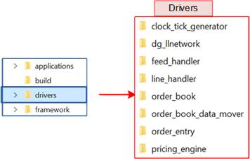
Figure 26 AAT-QDMA-LLIP Driver
The AAT-QDMA-LLIP Driver is a software layer for controlling and monitoring the hardware components of the AAT-QDMA-LLIP system. It performs write and read operations on hardware registers to enable configuration, status retrieval, and operational control.
The driver is organized into sub-drivers, each dedicated to a specific hardware block, such as the Clock Tick Generator, DataMover, or OrderEntry modules. Each sub-driver consists of a driver implementation and a corresponding shell. The driver layer provides low-level functions to interact with hardware registers, while the shell offers a high-level interface for user commands, simplifying configuration and debugging.
Compared with the AAT-QDMA system, the AAT-QDMA-LLIP modifies three drivers: DG LL-IP, LineHandler, and OrderEntry. This section provides detailed descriptions of these drivers, while the remaining drivers are identical to those in the AAT-QDMA system. Further details on the AAT-QDMA drivers can be found in Section 3.3 of the LL10GEMAC-IP with AAT-QDMA Demo Reference Design document.
3.3.1 Network Driver (DG LL-IP)
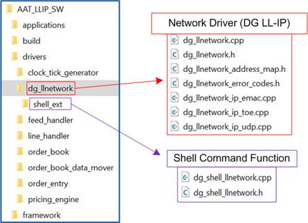
Figure 27 Network Driver
The Network Driver provides control over Design Gateway’s Low-Latency IP suite, enabling interaction with the LL10GEMAC-IP, UDP10GRx-IP, and TOE10GLL-IP. It performs register-level write and read operations to manage each network channel, including status retrieval and latch resets. The driver interfaces with hardware registers defined in “dg_llnetwork_address_map.h”, and error handling is defined in “dg_llnetwork_error_codes.h”. Core functionalities are separated into dedicated source files for each IP core: “dg_llnetwork_ip_emac.cpp” for LL10GEMAC-IP, “dg_llnetwork_ip_udp.cpp” for UDP10GRx-IP, and “dg_llnetwork_ip_toe.cpp” for TOE10GLL-IP. User interaction is handled through shell commands defined in “dg_shell_llnetwork.cpp”.
The Network Driver replaces the original Ethernet driver and TCP/UDP IP driver in the AAT-QDMA design, providing direct support for the Low-Latency IP suite.
The key files and their responsibilities are as follows:
· dg_llnetwork_address_map.h: Define the address variables mapped to hardware registers for write and read access in the DG-LLIP submodule of the target platform.
· dg_llnetwork_error_codes.h: Define the returned value for driver-layer functions, including both “OK” status and error codes. All function return values in this class reference these definitions.
· dg_llnetwork.h: Declare classes and functions used in the C++ source files, specifying which functions can or cannot be accessed by other classes.
· dg_llnetwork.cpp: Implement general functions for initialization, I/O management, kernel verification, and kernel reset control.
· dg_llnetwork_ip_emac.cpp: Implement functions for reading LL10GEMAC-IP status.
· dg_llnetwork_ip_udp.cpp: Implement functions for configuring UDP/IP network parameters, reading UDP10GRx-IP status, and managing UDP sessions.
· dg_llnetwork_ip_toe.cpp: Implement functions for configuring TCP/IP network parameters, reading TOE10GLL-IP status, and managing TCP sessions.
The Network Shell builds on the Network Driver functions to provide a command-line interface. The commands available in the shell for managing the network submodule are listed in Table 2.
Table 2 Network Shell Command
|
Command |
Argument |
Description |
|
getstatus |
<channel-option> |
Display the status of all channels, or a specific channel if provided. |
|
setconfigallowed |
<channel> <bool> |
Enable or disable configuration writes for the specified channel. |
|
setkernelreset |
<bool> |
Set or clear the reset state of the entire kernel. |
|
setmacaddr |
<channel> <macaddr> |
Set the source MAC address for the TCP/UDP interface on the channel. |
|
setipaddr |
<channel> <ipaddr> |
Set the source IP address for the TCP/UDP interface on the channel. |
|
setmcastmode |
<channel> <bool> |
Enable or disable multicast mode for the specified UDP channel. |
|
addtcpsession |
<channel> <ID> <dstipaddr> <dstport> <srcport> |
Creates a new TCP session with the specified parameters. |
|
deletetcpsession |
<channel> <ID> |
Delete the active TCP session associated with the given ID. |
|
deletetcpallsession |
<channel> |
Delete all TCP sessions on the specified channel. |
|
addudpsession |
<channel> <ID> <dstipaddr> <dstport> <srcport> <mcastaddr-option> |
Create a new TCP session with the specified parameters. |
|
deleteudpsession |
<channel> <ID> |
Delete the active UDP session associated with the given ID. |
|
deleteudpallsession |
<channel> |
Delete all UDP sessions on the specified channel. |
3.3.2 Line Handler Driver
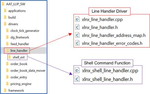
Figure 28 Line Handler Driver
The Line Handler software manages UDP multicast feeds by interacting with hardware control registers. It supports advanced configuration and monitoring capabilities, including multicast filter management, reliability modes, sequence timing, and debug features like traffic echoing. The main driver is implemented in “xlinx_line_handler.cpp”, while the shell commands for user interaction are defined in “xlnx_shell_line_handler.cpp”.
The Line Handler driver has been slightly modified from the original AAT-QDMA software to align with the current hardware design. The key changes in the driver and shell are summarized below.
· xlnx_line_handler_address_map.h
· Remove address variables for IP address and port number filters.
· Add support for UDP session ID filtering.
· xlnx_line_handler_error_codes.h
· Remove error codes related to IP address and port number filters.
· Add new error codes for UDP session ID filter validation.
· xlnx_line_handler.cpp and xlnx_line_handler.h
· Modify the add and delete functions to configure filter parameters using UDP session ID instead of IP address and port number.
· Update input verification functions to validate UDP session IDs.
· xlnx_shell_line_handler.cpp
· Remove IP address and port number filter parameters from “add” and “delete” commands, replacing them with the UDP session ID parameter. Input port and split ID parameters are still used.
· Update the “GetStatus” command to display a filter-parameter table containing input port, UDP session ID, and split ID. The IP address and port number fields are removed.
The shell layer utilizes the Line Handler driver functions to provide a command-line interface for filter configuration, status monitoring, and debugging. The available commands are summarized in Table 3.
Table 3 Line Handler Shell Command
|
Command |
Argument |
Description |
|
getstatus |
None |
Retrieve the Line Handler block status. |
|
add |
<inputport> <sessionID> <splitID> |
Add a multicast filter that associates a UDP session with a split ID on the specified port. |
|
delete |
<inputport> <sessionID> |
Delete a multicast filter for the given UDP session ID from the specified port. |
|
deleteall |
<inputport> |
Delete all multicast filters from the specified input port. |
|
setechoenabled |
<inputport> <bool> |
Enable or disable debug traffic echo for the specified port. |
|
setechodest |
<inputport> <sessionID> |
Set the UDP transmit session ID used for debug echo on the specified port. |
|
setsequencetimer |
<microseconds> |
Sets the cooldown interval for ignoring packets from the slower feed after a reset sequence number is received. |
|
resetsequence |
None |
Reset the sequence number. |
|
sethighreliability |
<bool> |
Enable or disable high-reliability mode. |
|
setspooltimerlimit |
<microseconds> |
Set the spool timeout limit (in us) before aborting. |
|
setspoolpacketlimit |
<numpackets> |
Set the maximum spool packet limit before aborting. |
3.3.3 Order Entry Driver
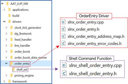
Figure 29 Order Entry Driver
The Order Entry Driver manages the creation and transmission of trading orders by interacting with hardware control registers. It supports configuring connections to remote systems, generating partial checksums, monitoring hardware status, and resetting statistical counters. The software can also read the last emitted message and establish or reconnect TCP connections. The driver implementation is in “xlnx_order_entry.cpp”, while user commands are defined in “xlnx_shell_order_entry.cpp”.
The Order Entry Driver has been slightly modified from the original AAT-QDMA software to align with the current hardware design. The key changes in the driver and shell are summarized below.
· xlnx_order_entry_address_map.h:
· Remove address variables for IP address and port number, replacing them with TCP session ID.
· Add new address variables for configuration control and debug status.
· Modify address values for transmission status and read-request statistics.
· xlnx_order_entry.cpp and xlnx_order_entry.h
· Modify the “Connect” and “Disconnect” functions to manage TCP connections using TCP session IDs instead of IP address and port number.
· Update the “GetConnectionDetails”, “GetTxStatus”, and “GetStats” functions, which report Order Entry module status.
· Add the “GetDebugValue” to read TCP connection status.
· xlnx_shell_order_entry.cpp
· Update the “Connect” command to replace IP address and port number parameters with the TCP session ID parameter.
· Modify the “GetStatus” command to display the TCP session IDs instead of the IP address and port number, and add new fields to support TOE10GLL-IP status.
· Remove the “ConnectionErrorCodeToString” function for generating error codes.
The Order Entry Shell commands provide a high-level interface for user interaction. Table 4 summarizes the available commands.
Table 4 Order Entry Shell Command
|
Command |
Argument |
Description |
|
getstatus |
None |
Displays the current Order Entry block status. |
|
readmsg |
None |
Read and print the last emitted FIX message. |
|
resetstats |
None |
Reset all Order Entry statistics counters. |
|
connect |
<sessionid> |
Establish a TCP connection to a remote system using the specified session ID. |
|
disconnect |
None |
Close the current TCP connection to the remote system. |
|
reconnect |
None |
Close and then re-open the existing TCP connection. |
|
setcsumgen |
<bool> |
Enable or disable partial checksum generation for outgoing messages. |
3.4 AAT-QDMA-LLIP Application
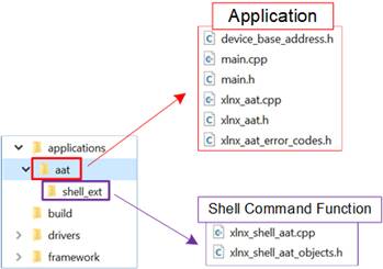
Figure 30 Application
The AAT-QDMA-LLIP Application provides a unified platform for controlling and monitoring hardware components through a command-based interface. It integrates various hardware drivers to offer seamless interaction between software and FPGA-based hardware for trading applications.
The application is divided into two key components. First is “Shell Command Interface”, a command-line interface for executing user-defined operations on the AAT-QDMA-LLIP system. Second is “Application” to manage the initialization, communication, and interaction with hardware components.
The application in this system is identical to the one used in the AAT-QDMA system. Further details are provided in Section 3.4 of the “LL10GEMAC-IP with AAT-QDMA Demo Reference Design” document:
https://dgway.com/products/IP/Lowlatency-IP/ll10gemac-ip-aat-qdma-refdesign-amd/
3.5 AAT-QDMA Script
The AAT-QDMA script consists of shell commands designed to configure all hardware and software components required for the system’s operation. These scripts ensure that each component is properly initialized and configured. The configuration is divided into two files:
· “demo_setup.cfg”: Configures the system for “Pricing Engine on Card” mode.
· “demo_setup_with_datamover.cfg”: Configures the system for “Pricing Engine on Software” mode, including DataMover setup and excluding hardware Pricing Engine configurations.
3.5.1 demo_setup.cfg
The “demo_setup.cfg” file contains commands to initialize and configure system components, including Network, LineHandler, FeedHandler, PricingEngine, OrderEntry, and ClockTick Generator. The key configurations are summarized below.
Network
The Network subsystem sets up communication parameters for Ethernet-based UDP and TCP connections. It consists of four channels:
· Channel 0: TCP egress (order transmission)
· Channels 1–2: UDP ingress (market data)
· Channel 3: Reserved for internal loopback
Example configurations:
· Channel 0 – TCP Egress
1) Channel 0 is configured with the local IP address “192.168.20.200”. This IP address identifies the FPGA as the source for TCP traffic used to transmit order messages.
>> network setipaddr 0 192.168.20.200
2) A TCP session is created on Channel 0 for order transmission. In this example, the FPGA connects to a host at IP address “192.168.20.100”, destination port “12345”, using local source port “10201”. The session is indexed as 0, allowing higher-level software (such as the Order Entry submodule) to reference and manage it.
>> network addtcpsession 0 0 192.168.20.100 12345 10201
· Channel 1 – UDP Ingress
1) Channel 1 is configured with the local IP address “192.168.10.200”. This IP address identifies the FPGA as the destination for incoming UDP packets on this channel.
>> network setipaddr 1 192.168.10.200
2) Multicast reception is enabled on Channel 1. This allows the channel to join and receive data from specified multicast groups. Without enabling this mode, multicast packets sent to the FPGA would be ignored.
>> network setmcastmode 1 true
3) Two UDP multicast sessions are configured to handle redundant market data feeds (commonly referred to as Line A and Line B) from different sources. These sessions improve reliability by ensuring that identical market data streams can be processed and compared.
· Line A: Receives data from source IP 205.209.221.75, source port 80, with destination port 14318, and joins multicast group 224.0.31.9.
· Line B: Receives data from source IP 205.209.212.75, source port 80, with destination port 15318, and joins multicast group 224.0.32.9.
>> network addudpsession 1 0 205.209.221.75 80 14318 224.0.31.9
>> network addudpsession 1 1 205.209.212.75 80 15318 224.0.32.9
Line Handler
The Line Handler configuration manages filters and timing parameters for processing UDP multicast feeds. It is responsible for handling A and B lines, setting up port filters, and configuring sequence timers. The example commands below demonstrate how to configure the Line Handler with explanations for each step:
1) Filters are added using the add command, which takes three arguments: <inputport> <sessionID> <splitID>. In this example, two filters are added for input port 0 with session IDs 0 and 1, both assigned to split ID 0:
>> linehandler add 0 0 0
>> linehandler add 0 1 0
2) The sequence timer is set to 1000 microseconds. This defines the cooldown interval after a sequence reset (sequence number = 0), during which packets from the slower feed are ignored to prevent acceptance of old sequence numbers.
>> linehandler setsequencetimer 1000
Feed Handler
The Feed Handler configuration manages the registration of Security IDs, which enables the system to process market data updates for specified securities. This ensures that only relevant data streams are decoded and forwarded for further processing.
Each registered Security ID corresponds to a particular ticker symbol or financial instrument in the market. In this example, several Security IDs—including 1024, 2048, 3072, and a large ID 305419896—are registered:
>> feedhandler add 1024
>> feedhandler add 2048
>> feedhandler add 3072
>> feedhandler add 4096
>> feedhandler add 5120
>> feedhandler add 6144
>> feedhandler add 7168
>> feedhandler add 8192
>> feedhandler add 9216
>> feedhandler add 10240
>> feedhandler add 305419896
Pricing Engine
The Pricing Engine configuration defines global trading strategies and enables global pricing mode for all securities. These settings ensure that trading logic is consistently applied across the entire system. Below are the commands and their explanations:
· Configures the global trading strategy to “peg” using the “setglobalstrategy” command. The “peg strategy” dynamically adjusts bid and ask prices based on changes in the top-of-book (ToB) price.
>> pricingengine setglobalstrategy peg
· Activate the global pricing mode using the “setglobalmode” command with the argument “true”. When enabled, global pricing mode applies the configured strategy to all securities.
>> pricingengine setglobalmode true
OrderEntry
The OrderEntry configuration establishes the connection to a remote system and optimizes data transmission efficiency by enabling hardware-based checksum generation. Below are the commands and their explanations:
1) Configures the OrderEntry to enable partial checksum generation using the “setcsumgen” command with the argument “true”. When enabled, the hardware offloads checksum calculations for TCP packets, reducing CPU overhead and improving transmission efficiency.
>> orderentry setcsumgen true
2) Sets up a connection to a remote system using the “connect” command with the specified channel. In this example, the system connects to channel 0.
>> orderentry connect 0
ClockTick Generator
The ClockTick Generator sets precise timing intervals for event streams, which synchronize hardware modules across the system. Below are the commands and their explanations:
1) Configures the interval for each clock tick event stream using the “setinterval” command. In this example, Stream 0 is configured with an interval of 1,000,000 microseconds (1 second).
>> clocktickgen setinterval 0 1000000
2) Activate a specific tick stream using the “setenable” command with the argument “true”. In this example, Stream 0 is enabled to start generating tick events.
>> clocktickgen setenable 0 true
The generator supports up to five event streams, which can be assigned to specific hardware modules as follows:
· Stream 0: Feed Handler
· Stream 1: OrderBook
· Stream 2: Pricing Engine
· Stream 3: OrderEntry
· Stream 4: Line Handler
3.5.2 demo_setup_with_datamover.cfg
The “demo_setup_with_datamover.cfg” file is largely similar to “demo_setup.cfg”, with the following key differences:
· Enable the transmission of OrderBook data to the software-based Pricing Engine.
· Disable the hardware Pricing Engine when operating in “Pricing Engine on Software” mode.
DataMover
The DataMover configuration transfers OrderBook data to the software Pricing Engine running on the host. Below are the commands and their explanations:
1) The “startdatamover” command initializes the DataMover submodule, allowing the OrderBook to forward data to the host for software-based processing.
>> aat startdatamover
2) The “threadstart” command activates the thread responsible for running the software Pricing Engine. This thread processes the data received from the OrderBook.
>> datamover threadstart
4 Target Software
The target system software uses “tcpreplay” as a market data generator. “tcpreplay” is an open-source network traffic generator that replays previously captured traffic from “pcap” (packet capture) files. It is widely used for testing and debugging network devices, applications, and security systems by simulating real-world traffic conditions.
In this design, “tcpreplay” replays the “cme_input_arb.pcap” file to simulate CME market data, allowing the AAT-QDMA-LLIP system to process and respond to market conditions as if operating in a live environment.
For more information about “tcpreplay”, visit the official website:
https://tcpreplay.appneta.com/
5 Revision History
|
Revision |
Date (D-M-Y) |
Description |
|
1.00 |
23-Sep-25 |
Initial version release |