LL10GEMAC-IP with AAT Calypte DMA Demo
Reference Design Manual
2.1.1 Transceiver (PMA for 10GBASE-R)
3.5.2 demo_setup_with_datamover.cfg
1 Introduction
High-Frequency Trading (HFT) is an advanced form of algorithmic trading where sophisticated computer programs execute a large number of orders at extremely high speeds, often within microseconds. This approach capitalizes on minute price discrepancies in financial markets, aiming to generate profits from rapid, short-term market movements.
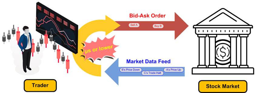
Figure 1 High-Frequency Trading (HFT) Scheme
The competitive landscape of HFT is predominantly defined by latency - the time delay between the initiation of a market event and the corresponding trading response. In this domain, even nanosecond-level advantages can significantly impact profitability. Consequently, HFT firms invest heavily in ultra-low-latency technologies to process market data and execute trades faster than their competitors.
Success in HFT hinges on the ability to swiftly analyze incoming market data and promptly submit bid-ask orders. Traders who can reduce latency in these processes are more likely to secure favorable trade positions, thereby enhancing their potential for substantial profits. This relentless pursuit of speed underscores the critical importance of low-latency systems in the HFT industry.
For maintaining a competitive edge in the trader system, various system architectures have been developed as shown in Figure 2.
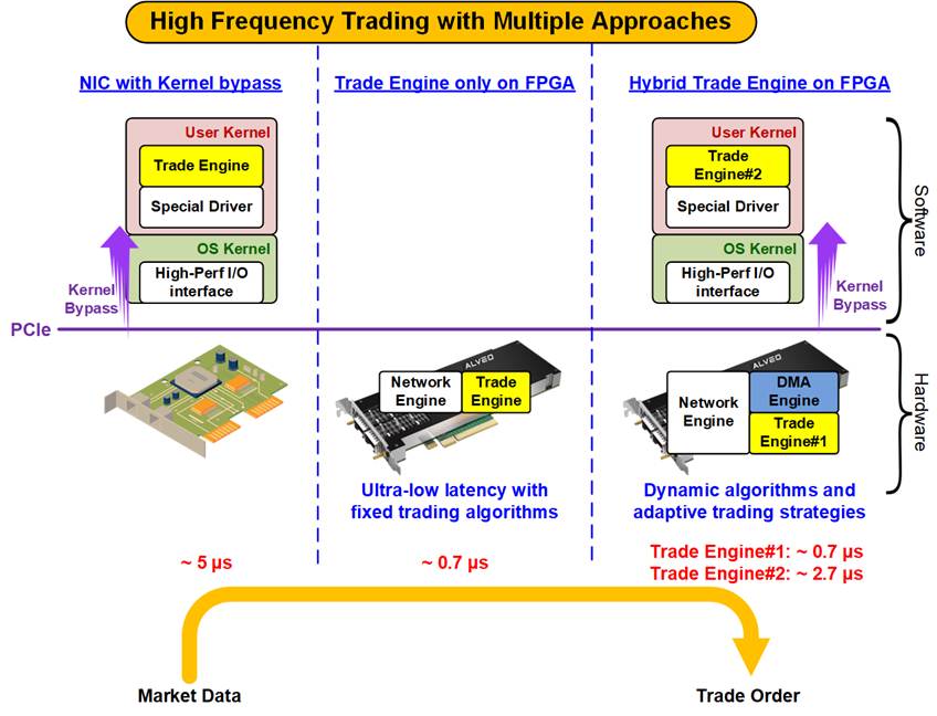
Figure 2 Trader System Approach for HFT
The first solution (leftmost in the figure) employs a specific Network Interface Card (NIC) with kernel bypass technology. This approach allows the NIC to bypass the operating system’s kernel and networking stack, minimizing overhead from kernel-level processing. By utilizing user-space drivers and high-speed I/O interfaces, this architecture typically achieves response latencies of approximately 5 microseconds. Implementations often adopt frameworks such as the Data Plane Development Kit (DPDK) to facilitate kernel bypass and improve performance.
In this initial approach, the majority of latency arises from data transfers between the NIC and the trading application via the PCIe interface. To reduce this latency, the second solution integrates trading algorithms directly into the FPGA, thereby eliminating the PCIe data transfer overhead. This configuration delivers an extremely low latency of around 700 nanoseconds. However, algorithms implemented entirely in FPGA logic offer limited flexibility and cannot be easily modified during operation. As a result, such systems are typically optimized for a limited number of markets or fixed trading strategies, making them less suitable for users who require more complex and adaptive algorithms.
To meet the requirements for both low latency and real-time algorithm adaptability, the third approach extends the data path between FPGA hardware and software applications by incorporating a specialized low-latency DMA engine within the FPGA. This architecture enables the trading system to support hybrid trading operations—executing ultra-low-latency trades directly on the FPGA for selected markets, while simultaneously allowing software-based trading for dynamic or complex algorithms. With the dedicated DMA engine, PCIe data transfer latency (round-trip time) can be reduced to about 2 microseconds, resulting in an overall system latency of approximately 2.7 microseconds for software-assisted trading.
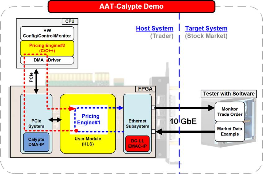
Figure 3 AAT-Calypte DMA System
This demonstration showcases a simplified implementation of the third approach, featuring two pricing engines—one implemented in FPGA logic and the other executed in Host software. The Pricing Engine represents a functional component of the overall trading engine, responsible for generating trading orders. The system comprises two main components: the Host and the Target.
The Host serves as the trader’s platform, typically a PC or server equipped with an FPGA card, while the Target functions as a simulated stock market. The Target software performs two key operations: transmitting sample market data to the Host and receiving Bid–Ask orders generated by either the FPGA trading engine or the Host software.
The following sections provide a detailed description of this demonstration system.
2 Host Hardware
The AAT-Calypte DMA framework connects the Host and Target systems through four 10G Ethernet channels. Two channels handle UDP Market Data from the Target, one channel manages TCP Bid-Ask Orders from the Host, and the remaining channel is reserved for loopback testing to measure latency. A minimum of two Ethernet channels is required to run the demo—one for UDP Market Data and one for TCP Orders. The Host system integrates an FPGA card as a hardware accelerator connected to the CPU system via a PCIe interface, while the Target system uses a standard PC running test software that communicates over Ethernet through a standard Network Interface Card (NIC).
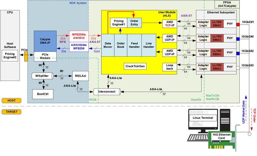
Figure 4 Host Hardware on AAT- Calypte DMA Demo
Figure 4 illustrates the Host hardware architecture, implemented in FPGA logic. This architecture comprises four main hardware blocks. The first block is the Ethernet Subsystem, responsible for handling low-layer networking across four Ethernet channels. It integrates Design Gateway's Low-Latency 10G Ethernet MAC IP Core (LL10GEMAC), which minimizes network latency in conjunction with AMD PHY. Design Gateway's adapter logic facilitates data width conversion and clock domain crossing between LL10GEMAC and the upper layers.
The second hardware block is the User Module, which integrates the Pricing Engine responsible for implementing the user’s trading algorithm. All submodules inside User Module are developed entirely using High-Level Synthesis (HLS), providing flexibility and adaptability across different trading markets. The HLS design is based on AMD reference design and incorporates a loopback module, TCP/UDP IP cores for upper-layer networking, and several trading sub-blocks, such as the Line Handler, Feed Handler, and Order Book.
Communication between the FPGA card and the Host CPU occurs via a PCI Express (PCIe) interface, optimized for ultra-low latency data transfer by DYNANIC through Calypte DMA IP. The Calypte DMA needs to operate with the Network Development Kit (NDK) system and the NFB framework driver developed by CESNET. Since the NDK bus interfaces are not compatible with the User Module interfaces, the adapter modules (MFB256toAXIS512, AXIS1024toMFB256, and MI2LAxi) are implemented to bridge these interface differences and ensure proper data flow.
The Host hardware operates across three primary clock domains. The MacTxClk/MacRxClk, derived from the AMD PHY, runs at 322.265625 MHz to support 10G Ethernet functionality. The UserClk domain drives the User Module, Calypte DMA, and PCIe module, serving as the main clock domain for data processing and transfer operations. Finally, the MiClk domain is dedicated to the Boot Controller in the NDK system, managing startup and flash operations.
As illustrated in Figure 4, once the Order Book is updated with processed market data, there are two possible data flow options for forwarding information to the trading strategy that determines the next trading action.
The first option passes the updated Order Book information directly to Pricing Engine#1, which evaluates the data using the configured trading strategy to determine the next trading action. The resulting trade decision is then sent to the Order Entry module. If trading conditions are met, Bid–Ask orders are generated and transmitted as TCP packets. In this configuration, the entire trading engine operates entirely within the FPGA fabric – referred to as the “Pricing Engine on Card” mode.
The second option forwards the updated Order Book data to the Data Mover, which transfers it to the Host software via a DMA operation. The software-based Pricing Engine#2, running on the Host CPU, performs complex computations or dynamic algorithmic processing. Once the calculations are complete, the results are transferred back to the FPGA through the Data Mover. The Data Mover subsequently forwards the processed results to the Order Entry module, where Bid–Ask orders are generated and transmitted. This configuration, which provides greater flexibility for implementing advanced or frequently changing trading strategies, is referred to as the “Pricing Engine on Software” mode.
The user can configure which Pricing Engine mode the Host will operate in. Subsequent sections provide detailed descriptions of each hardware module.
2.1 Ethernet Subsystem
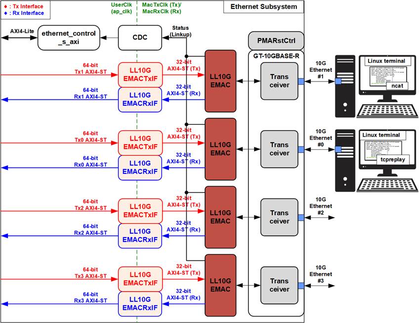
Figure 5 Ethernet Subsystem Block Diagram
To achieve 10G Ethernet connectivity with low latency, Design Gateway integrates the LL10GEMAC-IP with AMD 10G BASE-R PMA solutions. The FPGA cards used in this reference design feature two DSFP28 connectors, which can be split into four independent 10G Ethernet channels. As a result, the Ethernet Subsystem incorporates four Ethernet MAC interface sets to manage these connections.
The data interface of Ethernet Subsystem operates in the ap_clk domain, where the frequency can be adjusted to meet specific system requirements. In contrast, the user interface of the transceiver for 10GBASE-R operates in distinct clock domains: MacTxClk for the Tx interface and MacRxClk for the Rx interface. To ensure reliable communication and synchronization across these different clock domains, Clock Domain Crossing (CDC) logic is implemented.
The Ethernet Subsystem provides four interfaces, all using a 64-bit AXI4-Stream interface. The LL10GEMACTxIF module adapts data from the ap_clk domain to MacTxClk, reducing the data width from 64 bits to 32 bits for the transmit path. Conversely, the LL10GEMACRxIF module adapts data from MacRxClk to ap_clk, increasing the data width from 32 bits to 64 bits for the receive path. Both modules interface with the 10G Ethernet MAC controller (LL10GEMAC-IP) using a 32-bit AXI4-Stream interface (AXI4-ST) for transmit and receive operations.
The ethernet_control_s_axi module converts the AXI4-Lite interface to internal signals for write/read access and is mapped to the control and status signals of other modules. When signals cross different clock domains, CDC logic is applied to maintain synchronization. The Linkup status of all Ethernet connections is returned as a status signal by the LL10GEMAC-IP.
Further details of each module are described below.
2.1.1 Transceiver (PMA for 10GBASE-R)
The PMA IP core for 10G Ethernet (BASE-R) can be generated using Vivado IP catalog. In the AMD FPGA Transceivers Wizard, the user uses the following settings.
· Transceiver configuration preset : GT-10GBASE-R
· Encoding/Decoding : Raw
· Transmitter Buffer : Bypass
· Receiver Buffer : Bypass
· User/Internal data width : 32
· Include transceiver COMMON in the : Example Design (not include in Core)
Four channels are enabled in the AAT demo for four Ethernet connections. An example of the Transceiver wizard in Ultrascale model is described in the following link.
https://docs.amd.com/r/en-US/pg182-gtwizard-ultrascale/Example-Design
2.1.2 PMARstCtrl
When bypassing the buffer inside the AMD FPGA transceiver, the user logic must manage the reset signals for both the Tx and Rx buffers. This function is implemented using a state machine that follows the steps outlined below:
1) Assert Tx reset of the transceiver to 1b for one clock cycle.
2) Wait until Tx reset done, output from the transceiver, is asserted to 1b.
3) Finish Tx reset sequence and de-assert Tx reset, user interface output, to allow the user logic beginning Tx operation.
4) Assert Rx reset to the transceiver.
5) Wait until Rx reset done, output from the transceiver, is asserted to 1b.
6) Finish Rx reset sequence and de-assert Rx reset, user interface output, to allow the user logic beginning Rx operation.
2.1.3 DG LL10GEMAC
The IP core by Design Gateway implements low-latency EMAC and PCS logic for 10Gb Ethernet (BASE-R) standard. The user interface is 32-bit AXI4-Stream bus. Please see more details from LL10GEMAC-IP datasheet on our website.
https://dgway.com/products/IP/Lowlatency-IP/dg_ll10gemacip_data_sheet_xilinx_en/
2.1.4 LL10GEMACTxIF
The LL10GEMACTxIF module is an AXI4-Stream data adapter designed to interface with transmitting path of LL10EMAC. It performs clock domain crossing and data width conversion from 64 bits to 32 bits. This module is optimized for low-latency performance, but its operation is subject to certain limitations:
1) The ratio of MacTxClk frequency to UserClk frequency must be less than two.
2) If UserTxValid is dropped during transmission, an error is asserted to the Ethernet MAC, prompting it to cancel the current packet transmission. Packet retransmission is then initiated, so the transmission latency increases.
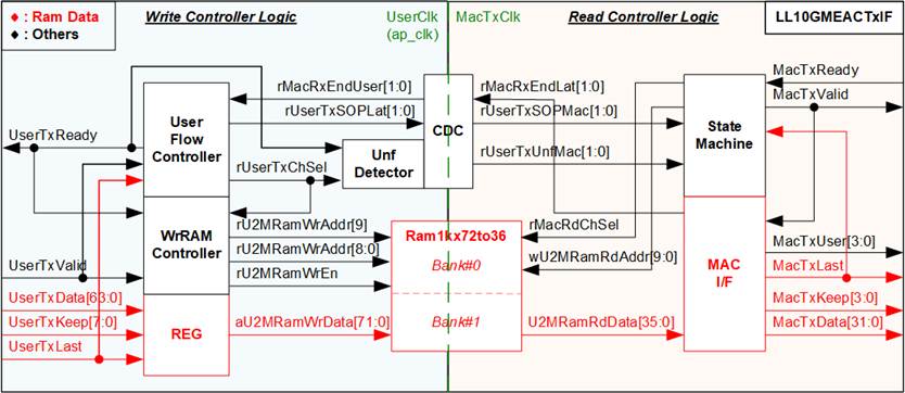
Figure 6 LL10GEMACTxIF Logic Diagram
As illustrated in Figure 6, the Ram1k72to36 module buffers the data stream between the User interface and the Ethernet MAC (EMAC). The Write controller logic operates in the UserClk domain, while the Read controller logic runs in the MacTxClk domain. Additionally, clock domain crossing (CDC) logic is implemented to transfer flow control signals across clock domains, i.e., Start-of-packet (UserTxSOP), Underflow flag (UserTxUnf), and End-of-packet (MacRxEnd).
Ram1kx72to36
Ram1kx72to36 is a block memory module configured as a simple dual-port block RAM type with an asymmetric data width feature. It stores 72-bit data in the UserClk domain and converts it to 36-bit data in the MacTxClk domain. The 36-bit data comprise 32-bit data, 2-bit encoded keep signal, 1-bit last flag, and 1-bit reserved signal.
The Ram1kx72to36 module is divided into two banks, enabling it to store two packet data from the user via the AXI4-Stream interface. The maximum packet size is limited to half the size of the RAM, which is 4096 bytes (equivalent to 512 entries of 64-bit data). The packet length can be increased by extending the RAM depth.
Write controller
The User flow controller asserts UserTxReady to accept a new packet transmission when the next RAM bank is available. The WrRAM Controller generates the write address to store data of each packet in the same RAM bank during transmission from user. After the final packet data is transferred, the MSB of the address is inverted to switch the active bank. Additionally, the User flow controller asserts the Start-of-frame flag (rUserTxSOPLat) when the first data of a new packet is received. This flag is forwarded to the Read controller via CDC to initiate packet transmission to the EMAC. Once the Read controller transfers the final packet data from a RAM bank, the End-of-frame flag (rMacRxEndLat) is asserted, signaling the User flow control to free the RAM.
Due to the EMAC limitation, each
packet must be transmitted entirely without pauses. To meet this requirement,
the data in RAM must always be ready for reading, and the Write controller must
write data to RAM continuously until the end of packet. An Unf detector is included
to monitor for interruptions during packet transmission. If the user pauses the
transmission by de-asserting UserTxValid to 0b before completing the final
packet data transfer, the Unf detector asserts the Underflow flag
(rUserTxUnfLat). This signal is also sent to the Read controller via CDC to
cancel the packet transmission on the EMAC interface.
Read controller
The State machine manages the data flow, forwarding read data from the RAM to the EMAC. MacTxValid is asserted to 1b when the State machine detects the Start-of-frame flag for a new packet. The read address is created by the State machine to read RAM data, which includes 32-bit data, keep data, and the last flag.
The MAC I/F includes a decoder that converts the 2-bit encoded keep signal into a 4-bit signal. If the Underflow flag is asserted before the final data is transmitted, the State machine asserts MacTxLast and MacTxUser to cancel the current packet transmission. Following this, the State machine initiates packet retransmission by reading the first data of the same RAM bank. Once the final packet data is transmitted successfully, the State machine switches to the next RAM bank for the subsequent packet transmission.
Figure 7 and Figure 8 illustrate the timing diagram of the Write Controller, covering both normal and underflow conditions. The following information further details on the timing diagram.
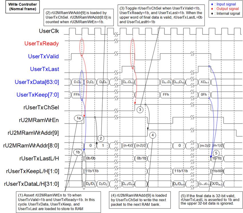
Figure 7 Write Controller of LL10GEMACTxIF Timing Diagram (Normal Case)
1) When UserTxValid is set to 1b to transmit 64-bit data stream via the AXI4-Stream interface, the Write Controller asserts UserTxReady to 1b to accept data. The User data (UserTxData), User byte enable (UserTxKeep), and User last flag (UserTxLast) are stored in rUserTxDataL/H, rUserTxKeepL/H, and rUserTxLastL/H, respectively, while the write enable signal (rU2MRamWrEn) is set to 1b. To reduce the RAM data width, the 8-bit UserTxKeep signal is encoded into two 2-bit values (UserTxKeepL/H) according to the following mapping.
Table 1 UserTxKeepL/H Encoding Table
|
UserTxKeep[7:0] |
UserTxKeepL[1:0] |
UserTxKeepH[1:0] |
Description |
|
01h |
00b |
Not use |
UserTxData[7:0] is valid. |
|
03h |
01b |
UserTxData[15:0] is valid. |
|
|
07h |
10b |
UserTxData[23:0] is valid. |
|
|
0Fh |
11b |
UserTxData[31:0] is valid. |
|
|
1Fh |
11b |
00b |
UserTxData[39:0] is valid. |
|
3Fh |
11b |
01b |
UserTxData[47:0] is valid. |
|
7Fh |
11b |
10b |
UserTxData[55:0] is valid. |
|
FFh |
11b |
11b |
UserTxData[63:0] is valid. |
The 72-bit write data to RAM is assigned as follows.
· Bit[31:0] : rUserTxDataL
· Bit[33:32] : rUserTxKeepL
· Bit[34] : rUserTxLastL
· Bit[35] : Reserved
· Bit[67:36] : rUserTxDataH
· Bit[69:68] : rUserTxKeepH
· Bit[70] : rUserTxLastH
· Bit[71] : Reserved
The MSB of the RAM write address (rU2MRamWrAddr[9]) indicates the active RAM bank and is loaded from rUserTxChSel. rU2MRamWrAddr[8:0] is reset to 0 when storing the first packet data.
2) Once each data word is written to RAM (rU2MRamWrEn = 1b), rU2MRamWrAddr[8:0] increments to store the next incoming data word in sequence.
3) When the final packet data is received (UserTxValid=1b, UserTxLast=1b, and UserTxReady=1b), the bank indicator (rUserTxChSel) toggles to switch the active bank.
When UserTxLast is set to 1b to store the final packet data, rUserTxLastH is set to 1b. However, the value of rUserTxLastL depends on UserTxKeep. If UserTxKeep[7:4] ≠ 0, indicating that the final 32-bit data is stored in the upper word, rUserTxLastL is set to 0b.
4) rU2MRamWrAddr[9] toggles its value to select alternate RAM bank for the next packet.
5) If the upper 32-bit portion of the final packet is invalid (UserTxKeep[7:4]=0b), rUserTxLastL is asserted to 1b, indicating that the final data is positioned on the lower 32-bit word.
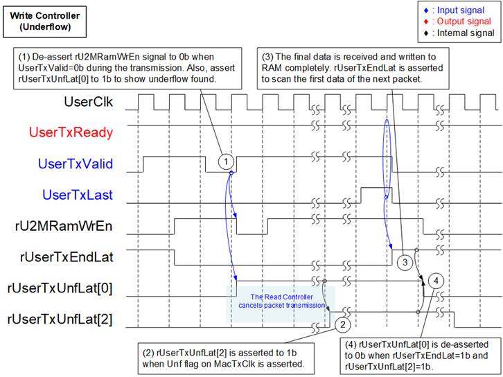
Figure 8 Write Controller of LL10GEMACTxIF Timing Diagram (Underflow Case)
Figure 8 illustrates the assertion of the Underflow flag to cancel an ongoing packet transmission when UserTxValid is de-asserted to 0b before the completion of the packet. In such cases, the packet must be retransmitted. For retransmission, the Underflow flag asserted by the Write controller is forwarded to the Read controller to halt the current packet transmission. Further details about this retransmission process within the Read Controller are provided in Figure 10.
1) Data from the user is always stored in RAM by asserting rU2MRamWrEn to 1b when both UserTxValid and UserTxReady are set to 1b. However, if UserTxValid is set to 0b before the reception of the final packet data (UserTxEndLat=0b), the Underflow Flag (rUserTxUnfLat[0]) is asserted to 1b.
Note: Although rUserTxUnfLat is asserted, all incoming packet data from the user continues to be stored in RAM until the operation is complete.
2) The Underflow flag (rUserTxUnfLat[0]) is forwarded via a Clock Domain Crossing (CDC) to assert the corresponding Underflow flag in the MacTxClk domain. Upon receiving this signal, the Read controller cancels the ongoing packet transmission and initiates packet retransmission. At this point, rUserTxUnfLat[2] is also asserted to 1b, indicating that the Read controller has acknowledged the cancellation request and initiated retransmission.
3) Once the final packet data is received (UserTxLast=1b, UserTxValid=1b, and UserTxReady=1b), rUserTxEndLat is asserted to 1b.
4) The Underflow flag (rUserTxUnfLat[0]) is de-asserted to 0b after the final packet data is received (rUserTxEndLat=1b) and the packet cancellation request has been fully acknowledged by the Read controller (rUserTxUnfLat[2]=0b).
Figure 9 presents the timing diagram of the Read Controller under normal operating conditions. The following steps describe the timing behavior in detail.
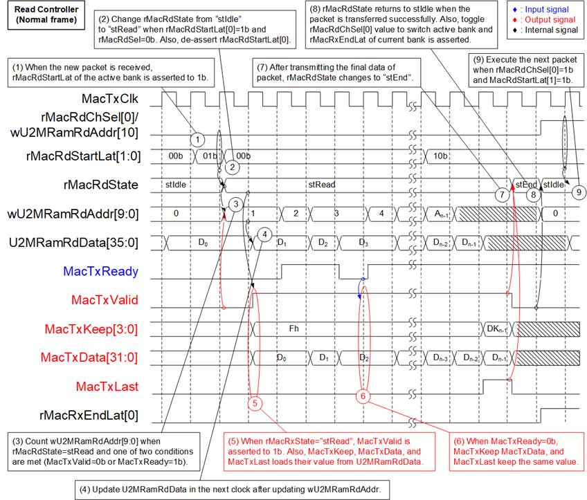
Figure 9 Read Controller of LL10GEMACTxIF Timing Diagram (Normal Case)
1) The Start flag (rMacRdStartLat) is asserted to 1b by the Write controller and transferred to the Read controller via CDC. This flag indicates the arrival of a new packet and prompts the Read controller to initiate processing.
2) If the Start flag of the currently active bank is asserted (rMacRdStartLat[0]=1b when rMacRdChSel[0]=0b), the state transitions from Idle (“stIdle”) to Read (“stRead”).
Note: rMacRdChSel[0] indicates the active bank (e.g., 0b for Bank#0 and 1b for Bank#1).
3) The read address (wU2MRamRdAddr[9:0]) is initialized to 0. It increments when the main state is Read state (rMacRdState=stRead), along with one of two following conditions: MacTxValid=0b (loading the first packet data) or MacTxReady=1b (Ethernet MAC acknowledges data transmission). The address is updated using combinational logic, ensuring synchronization with the same clock cycle as MacTxValid=0b or MacRxReady=1b. The MSB (wUMRamRdAddr[10]) corresponds to the channel indicator (rMacRdChSel), selecting RAM bank.
4) After the read address (wUMRamRdAddr[10:0]) is updated, the corresponding read data becomes available.
5) In “stRead”, the MacTxValid signal is asserted to 1b and the 36-bit data output from RAM (U2MRamRdData) is forwarded to the MAC interface as follows: (Bit[31:0]=MacTxData, Bit[33:32]=Encoded MacTxKeep, Bit[34]= MacTxLast).
The MacTxKeep encoding follows this mapping: 00b = 0001b, 01b = 0011b, 10b = 0111b, and 11b = 1111b.
6) If the EMAC is not ready to accept data (MacTxReady=0b and MacTxValid=1b), maintain the current values of MacTxKeep, MacTxData, and MacTxLast until the EMAC becomes ready.
7) After the final packet data is transmitted to the EMAC (MacTxValid=1b and MacTxLast=1b), the state transitions to “stEnd”.
8) In “stEnd”, the state waits until MacTxValid is de-asserted to 0b, indicating that entire packet data has been fully transmitted. The state then returns to “stIdle”, awaiting the next transfer. During this transition, the active bank is switched by toggling rMacRdChSel[0], and the End transfer flag (rMacRxEndLat) is asserted. The End flag is sent back to the Write controller to release the RAM for storing newly received packets from the user.
9) Returns to step (1), waiting for rMacRdStartLat of the active bank to be asserted and switch the active bank (rMacRdChSel[0]=1b), ensuring that the Read controller is prepared for the next packet transmission in the updated bank.
Figure 10 presents the timing diagram of the Read Controller under underflow operating conditions.
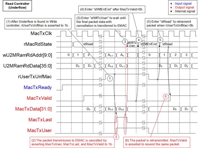
Figure 10 Read Controller of LL10GEMACTxIF Timing Diagram (Underflow Case)
1) When the Write controller detects that the user de-asserts UserTxValid to 0b before transmitting the final packet data, the Underflow flag in the MacTxClk domain (rUserTxUnfMac) is asserted to 1b.
2) In “stRead”, if rUserTxUnfMac is asserted to 1b, the ongoing packet transmission to the EMAC is halted by asserting MacTxValid, MacTxLast, and MacTxUser to 1b. When MacTxUser is asserted at the end of the packet, the EMAC terminates the transmission with an error condition directed to the target, causing the target to discard this packet.
3) The state machine transitions to “stWtTxUser”, waiting for the packet data completely transmitted to the EMAC.
4) The state machine verifies the successful completion of the error-handling process by detecting the de-assertion of MacTxValid to 0b. Once confirmed, the state changes to “stWtErrEnd”.
5) In “stWtErrEnd”, the state machine waits until the Underflow flag (rUserTxUnfMac) is de-asserted to 0b. Afterward, it transitions back to “stRead” to initiate packet retransmission.
6)
Once retransmission begins, MacTxValid
is re-asserted to resume normal packet transmission.
2.1.5 LL10GEMACRxIF
The LL10GEMACRxIF module serves as an AXI4-Stream data adapter interfacing with the receiving path of LL10GEMAC. It performs clock domain crossing for AXI4-stream and converts the data width from 32 bits to 64 bits. The module comprises several components: AXI4-ST 32bto64b Converter, Error Detection, AsyncFWFTFifo32x69, and AXI4-ST Read Controller.
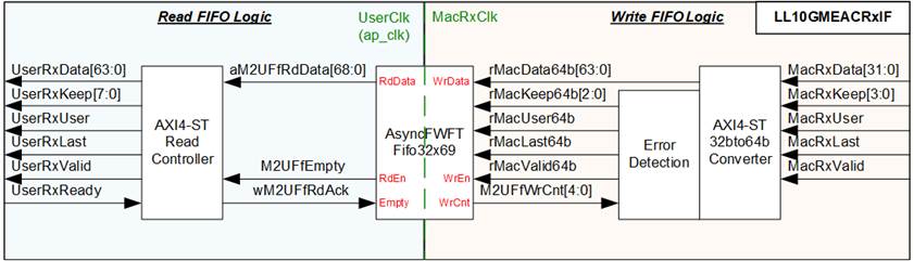
Figure 11 LL10GEMACRxIF Logic Diagram
The AXI4-ST 32bto64b Converter handles data width conversion from 32 bits to 64 bits and writes the data into the AsyncFWFTFifo32x69 module. Error Detection cancels the write operation in two cases: if the received packet size exceeds 9014 bytes, or if the available FIFO space drops below the threshold value of 8 data. When an error is detected, rMacUser64b, rMacLast64b, and rMacValid64b are asserted to 1b, marking the completion of the current packet transmission with an error status.
The AsyncFWFTFifo32x69 module functions as an asynchronous FWFT FIFO, storing data in the MacRxClk domain and transferring it to the UserClk domain. It handles 69-bit data, which includes 64 bits for data, 3 bits for encoded keep signal indicating 1-8 valid bytes, 1 bit for an error flag, and 1 bit for a last flag.
The AXI4-Stream Read Controller reads data from the AsyncFWFTFifo32x69 and forwards it to the user as AXI4-Stream data. Data is read only when the FIFO is not empty, and either the user is ready to receive data or the current data is the first packet data for transmission.
Figure 12 illustrates the timing diagram for writing to the FIFO inside LL10GEMACRxIF. The following details provide a description of the timing diagram.
1) The rWordHEn signal indicates the position of data stored in the 64-bit register (rMacData64b): 0b-lower 32-bit data, 1b-upper 32-bit data. It is initially set to 0b and toggled upon receiving each 32-bit data.
The keep signal, which represents byte validity for the 64-bit data, is encoded into a 3-bit signal (rMacKeep64b) according to the following mapping:
· MacRxKeep[3:0] -> rMacKeep64b[1:0]: 0001b->00b, 0011b->01b, 0111b->10b, and 1111b->11b.
· The value of rMacKeep64b[2] is determined by rWordHEn.
2) When the upper 32-bit data (rMacData64b[64:32]) is loaded, the 64-bit data (rMacData64b), 3-bit keep (rMacKeep64b), 1-bit error flag (rMacUser64b), and 1-bit last flag (rMacLast64b) are written to the FIFO by asserting rMacValid64b to 1b.
3) If the EMAC pauses data transmission by de-asserting MacRxValid to 0b, the values of rWordHEn, rMacData64b, and rMacKeep64b maintain their value until transmission resumes.
4) When the final packet data is transferred (MacRxValid=1b and MacRxLast=1b), MacRxKeep[3:0] is encoded to indicate the byte validity of the final data which resides in either the lower or upper 32-bit portion of the word.
· Upper 32-bit data (MacRxLast=1b, MacRxValid=1b, and rWordHEn=1b): The final packet data is stored in rMacData64b[63:32] and rMacKeep64b[2] is asserted to 1b.
·
Lower 32-bit data (MacRxLast=1b,
MacRxValid=1b, and rWordHEn=0b): The final packet data is stored in rMacData64b[31:0]
and rMacKeep64b[2] is de-asserted to 0b. The rWordHEn remains 0b after
receiving the final data.
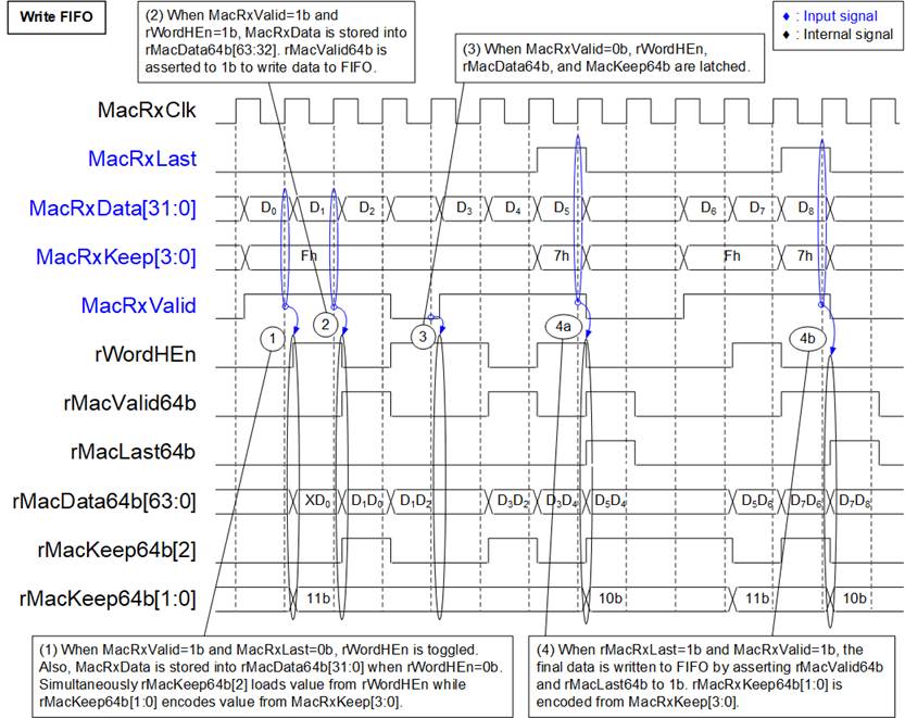
Figure 12 Write FIFO Logic of LL10GEMACRxIF Timing Diagram
Figure 13 presents the timing diagram of the AXI4-Stream Read Controller. The following details provide a description of the timing diagram.
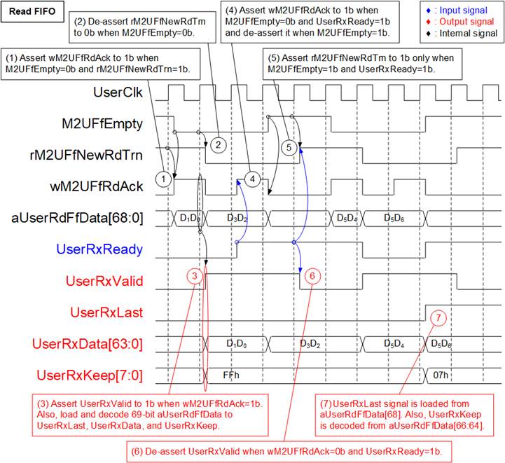
Figure 13 Read FIFO Logic of LL10GEMACRxIF Timing Diagram
1) Initially, rM2UFfNewRdTrn is set to 1b, indicating that no remaining data is stored in the internal latch register. If data is available in the FIFO (M2UFfEmpty=0b), the FIFO read enable (wM2UFfRdAck) is set to 1b. Since the FIFO is the FWFT type, the read FIFO data (aUserRdFfData) becomes valid in the same cycle that wM2UFfRdAck is asserted to 1b.
2) Once the FIFO data is stored in the internal latch register (indicated by M2UFfEmpty=0b), rM2UFfNewRdTrn is reset to 0b.
3) After a FIFO read operation (wM2UFfRdAck=1b), the FIFO output is transferred to the user interface with asserting UserRxValid to 1b. The AXI4-Stream data (UserRxData[63:0]) and the last flag (UserRxLast) are loaded from aUserRdFfData[63:0] and aUserRdFfData[68], respectively. While the keep signal (UserRxKeep[7:0]) is decoded from aUserRdFfData[66:64] using the following mapping: 000b -> 01h, 001b -> 03h, 010b -> 07h, 011b -> 0Fh, 100b -> 1Fh, 101b -> 3Fh, 110b -> 7Fh, and 111b -> FFh.
4) While rM2UFfNewRdTrn=0b (internal valid data stored in the internal latch), the FIFO is read (wM2UFfRdAck=1b) whenever FIFO has data (M2UFfEmpty=0b) and the user is ready to receive data (UserRxReady=1b).
5) When no data remains in the internal latch (UserRxReady=1b and M2UFfEmpty=1b), rM2UFfNewRdTrn is re-asserted to 1b, returning to step (1).
6) At this point, UserRxValid is de-asserted to 0b, pausing data transmission.
7) The last flag (UserRxLast) is asserted to 1b when aUserRdFfData[68]=1b. During transmission of the final packet data, UserRxKeep may be equal to 01h, 03h, 07h, …, FFh, indicating the valid bytes of the final data.
2.2 User Module
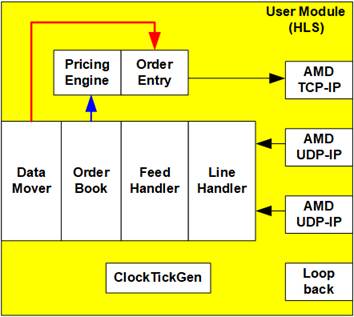
Figure 14 User Module Component
The User Module comprises several submodules developed using High-Level Synthesis (HLS) to minimize development time. These submodules are based on the AMD Accelerated Algorithmic Trading Demo. However, the DataMover submodule has been specifically modified to interface with the Calypte DMA-IP instead of XDMA-IP, ensuring compatibility with the system’s PCIe data transfer infrastructure.
Market data could be transmitted over two Ethernet channels using the UDP/IP protocols. The UDP payloads from both channels carry duplicate data to enable recovery in case of packet loss. The Line Handler manages packet duplication and loss to produce a single stream. This stream is then decoded by the Feed Handler and other submodules that follow the CME MDP 3.0 Market Data Protocol. This protocol uses the Financial Information Exchange (FIX) format with Simple Binary Encoding (SBE).
By leveraging HLS, users can easily develop, replace, or modify these submodules to support specific trading strategies and market requirements. Detailed descriptions of each submodule within the User Module are provided in the following sections.
2.2.1 UDP
This UDP submodule implements a UDP stack to enable data transmission over a UDP/IP connection, providing hardware-based networking capabilities tailored for trading systems. During initialization, the Host software configures key network parameters, including the IP address, subnet mask, and UDP listening ports, using the AXI4-Lite interface.
Packets with a matching target UDP port are processed, and the payload data is forwarded to the Line Handler submodule for further processing. The UDP submodule supports features such as multicast transmission, ARP and ICMP packet transmission for efficient data handling in real-time trading environments.
2.2.2 Line Handler
The Line Handler submodule is designed to arbitrate between two UDP streams, referred to as the A Line and B line which are linked to UDP#0 and UDP#1, to ensure reliable data delivery. Many stock exchanges deliver data feeds via UDP multicast, a high-speed but unreliable method where packets can be lost or delivered out of order. By subscribing to two identical multicast streams, the Line Handler ensures data integrity through line arbitration.
The Line Handler uses sequence number embedded in the packet headers to track and process incoming packets. This module outputs a single, reliable stream of market data for subsequent processing by the Feed Handler submodule.
2.2.3 Feed Handler
The Feed Handler submodule processes arbitrated UDP market data received from the Line Handler and decodes the messages according to the CME Market Data Protocol (MDP). This module specifically handles the feed for reporting the highest bid and lowest ask prices for up to five levels in the order book.
Messages received by the Feed Handler are formatted using the FIX protocol and encoded in Simple Binary Encoding (SBE). The submodule decodes these messages, and extracts key trading information such as price levels and bid/ask quantities. After updating securities information, the results are then passed to the Order Book submodule to maintain an up-to-date market view.
2.2.4 OrderBook
The OrderBook submodule maintains a five-level order book for both bid and ask sides. Each level contains aggregated quantities, prices, and the number of orders at specific price points. This submodule processes updates from the exchange feed, recalculates the order book, and ensures accurate market representation.
The submodule receives update instructions such as add, modify, or delete operations. It retrieves the current state of the order book from memory, applies the specified update, and reorders entries if necessary. Updated order book is then forwarded to either the Pricing Engine Submodule for on-card bid-ask order generation or the DataMover Submodule for transfer to the host memory. This dual-output capability supports both On-Card mode and Software mode configurations for the Pricing Engine.
2.2.5 DataMover
The DataMover submodule handles data transfer in both uplink and downlink of Calypte DMA-IP. The uplink transfers the updated OrderBook data while the downlink transfers the trade information to the OrderEntry submodule. The DataMover is enabled when the Pricing Engine is implemented by Host software.
Two components are implemented in DataMover for handling data transfer in each direction: responseMove for uplink transfer and operationMove for downlink transfer, as shown in Figure 15.
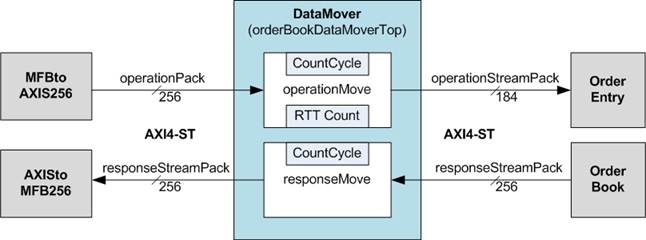
Figure 15 DataMover Submodule
responseMove
The responseMove module manages data flow between two AXI4-Stream interfaces. It forwards 256-bit responseStreamPack data from the OrderBook to the Calypte DMA IP.
Figure 16 illustrates the data structure of responseStreamPack.
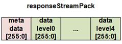
Figure 16 responseStreamPack Data Structure
As shown in Figure 16, responseStreamPack consists of six 256-bit data: one metadata word followed by five data level words (level0 to level4). The detailed descriptions of the metadata and data level fields are provided below.
· metadata: The meta data word contains general information for the OrderBook data stream.
- Bits[63:0] : Timestamp field. In this demo, the OrderBook always sets this value to zero.
- Bits[71:64] : Symbol index field. In this demo, the OrderBook always sets this value to zero.
- Bits[79:72] : The number of OrderBook levels following this metadata. In this demo, this value is fixed to 5, meaning that five data levels (level 0-4) are always output from the OrderBook.
· data level0 – data level 4: Each data level represents one OrderBook price level for the symbol indicated by metadata[71:64]. All data levels share the same six fields described below.
Note: A data level corresponds to a single price level in the OrderBook. For each level, bid fields describe buy-side orders, and ask fields describe sell-side orders.
- Bits[31:0] : bitCount field. Number of individual bid (buy) orders at this price level.
- Bits[63:32] : bitPrice field. Bid price of this level, representing the price at which buy orders are placed.
- Bits[95:64] : bitQuantity field. Total bid quantity at this price level. This value is the sum of quantities of all bid orders counted in bidCount.
- Bits[127:96] : askCount field. Number of individual ask (sell) orders at this price level.
- Bits[159:128] : askPrice field. Ask price of this level, representing the price at which sell orders are placed.
- Bits[191:160] : askQuantity field. Total ask quantity at this price level. This value is the sum of the quantities of all ask orders counted in askCount.
The operation of responseMove is controlled by three sequential state machines: IDLE, METADATA, and DATA.
· IDLE: Waits for a new metadata packet from the OrderBook. Upon receiving metadata, the state transitions to METADATA.
· METADATA: Decodes the metadata packet and replaces the timestamp field with the current value retrieved from CountCycle parameter inside responseMove module. This timestamp is later used by operationMove to calculate the round-trip time when a response packet is received through the Calypte DMA IP.
The updated 256-bit metadata is then forwarded to the DMA IP via the responseStreamPack interface. After transmission, the state transitions to DATA.
· DATA: Receives data level packets for the five fixed levels (level 0 to level 4) from the OrderBook and forwards them to the DMA IP. Once all levels are transmitted, the state transitions back to IDLE to await the next metadata packet.
operationMove
The operationMove module manages data flow between two AXI4-Stream interfaces:
· operationPack: A 256-bit AXI4-Stream interface that receives trade operation data from the Pricing Engine in the Host system via the Calypte DMA IP.
· operationStreamPack: A 184-bit AXI4-Stream interface that forwards only the required fields extracted from operationPack, with unused field removed.
The data structure of the 256-bit operationPack interface is defined as follows:
· Bits[7:0] : direction field. Indicates the order side: Bid (buy) or Ask (sell).
· Bits[39:8] : price field. Specifies the price of the order.
· Bits[71:40] : quantity field. Specifies the quantity of the order.
· Bits[103:72] : orderId field. Identifies the order ID.
· Bits[111:104] : symbolIndex field. Identifies the symbol associated with this order.
· Bits[119:112] : opCode field. Specifies the operation type, such as add, modify, or delete.
· Bits[183:120] : timestamp field. Timestamp associated with this trade operation.
· Bits[256:184] : unused field.
The operationMove module handles downlink trade operations by transferring trade operation data from the Host system to the OrderEntry module.
Because the Calypte DMA IP is configured with a 256-bit data width, incoming packets always have a width of 256 bits. However, only the lower 184 bits contain valid trade operation information. The upper bits [255:184] contain dummy data and are discarded. The valid 184-bit payload is forwarded to the OrderEntry via the operationStreamPack interface.
The operationMove module also supports round-trip time (RTT) measurement in conjunction with responseMove. The RTT calculation process is described below:
1) The packet output from responseMove contains a timestamp field corresponding to the CountCycle value inside the responseMove module.
2) The Pricing Engine in the Host system processes the packets received from the DataMover via the responseStreamPack interface and generates a trade operation response. This response is sent back to the DataMover via the operationPack interface and includes the timestamp extracted from the corresponding responseStreamPack packet.
3) Upon receiving the trade operation packet, operationMove extracts the timestamp and calculates the round-trip time by subtracting the received timestamp from the current value of the CountCycle counter inside the operationMove module.
Note: The CountCycle counters in responseMove and operationMove are implemented independently. However, they are synchronized by being reset to zero simultaneously at the start of operations to ensure accurate RTT measurement.
2.2.6 Pricing Engine
The Pricing Engine submodule is responsible for generating bid-ask orders for specific ticker symbols based on the current state of the market and configured trading rules. It operates on updates received from the OrderBook submodule, recalculating trading actions whenever changes occur.
The Pricing Engine submodule evaluates trading conditions and generates bid/ask requests, which are then forwarded to the OrderEntry submodule for execution. It also logs generated requests, providing visibility into executed strategies for analysis.
The submodule is configurable, allowing the updates to trading strategies, rules, and parameters. This flexibility supports rapid adaptation to changing market conditions.
2.2.7 OrderEntry
The OrderEntry submodule processes order placement requests received from the Pricing Engine or DataMover submodules. It constructs order messages in the FIX4.2 protocol format, including tags for price, quantity, order ID, and action type.
After constructing the order message, the OrderEntry submodule calculates and appends a partial checksum. The resulting message is then forwarded to the TCP submodule, which completes encapsulation by adding IP and TCP headers before transmitting the packet over the Ethernet interface.
2.2.8 TCP
The TCP submodule implements a TCP stack to establish and maintain TCP connections for transmitting order messages to a stock trading exchange. It supports up to 32 concurrent TCP connections using on-chip memory, with each connection allocated a 64 KB buffer for transmit and receive operations.
This submodule is closely integrated with the OrderEntry submodule, which generates order messages to be encapsulated with TCP headers and transmitted over the network. The TCP submodule also provides packet retransmission mechanisms to ensure reliable delivery and optimize performance in high-frequency trading environments.
During initialization, the Host system configures key network parameters, such as the MAC address and IPv4 address, via the AXI4-Lite interface. For data transfer, the TCP submodule receives commands and payload data from the OrderEntry submodule and transmits order packets to the target system.
2.2.9 ClockTick Generator
The ClockTick Generator submodule generates periodic pulse signals to synchronize and trigger operations across multiple submodules. During initialization, the Host system configures the generator via the AXI4-Lite interface, specifying time intervals in microseconds for each submodule.
The ClockTick Generator distributes timing signals to various components, including the Feed Handler, OrderBook, Pricing Engine, OrderEntry, and Line Handler. By providing these timing signals, it ensures coordinated processing and supports time-based execution of trading algorithms and system tasks, enabling synchronization across the hardware pipeline.
2.2.10 Loopback
The Loopback submodule provides a pass-through mechanism for Ethernet packets, enabling verification of data paths and measurement of system latency. This submodule receives Ethernet packets from the Rx AXI4-Stream interface (10GbE#3) and conditionally forwards them to the Tx AXI4-Stream interface (10GbE#3) based on a control register setting.
2.3 NDK System
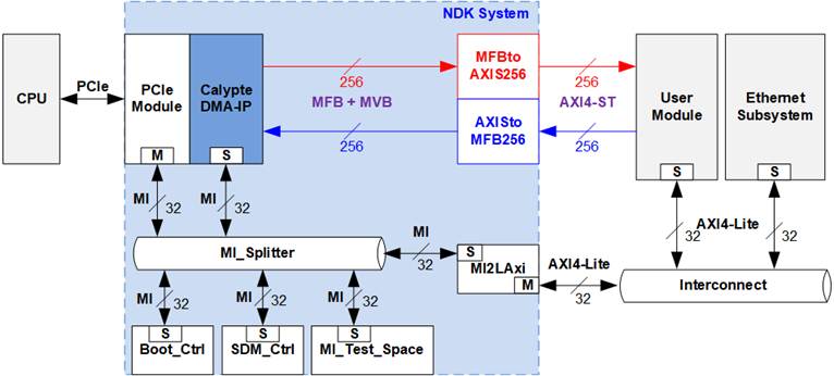
Figure 17 NDK System Component
The Calypte DMA facilitates ultra-low-latency data transfer between the FPGA and the Host system via the PCI Express (PCIe) interface. It operates within the NDK (Network Development Kit) platform, which includes the PCIe Module, MI_Splitter, Boot_Ctrl, SDM_Ctrl, and MI_Test_Space modules.
The Calypte DMA uses MFB (Multi-Frame Bus) and MVB (Multi-Value Bus) interfaces to transfer packet data and associated metadata. These interfaces differ from those used by the User Module, which relies on the standard AXI4-Stream (AXI4-ST) interface for data transfer and AXI4-Lite for control and status signals.
To ensure interface compatibility, two dedicated adapter modules, MFBtoAXIS256 and AXIStoMFB256, are implemented to bridge the data paths between the Calypte DMA and the User Module. Similarly, for register access, the MI2LAxi adapter module converts the MI bus used in the NDK platform into the AXI4-Lite interface employed by the User Module. This conversion enables seamless control and configuration of FPGA submodules through a unified bus interface.
For more details on the NDK platform and its internal interface, refer to the following link:
https://cesnet.github.io/ndk-fpga/devel/index.html
2.3.1 Calypte DMA.
The Calypte DMA provides a Direct Memory Access (DMA) solution optimized for PCIe communication. Its architecture is designed with a primary focus on achieving minimal latency, enabling full-duplex transmission of packet data between the FPGA and the Host memory.
The Calypte DMA connects to the surrounding NDK infrastructure through the MFB interface, which supports configurable bus widths and data structures. In this reference design, the MFB interface is configured as shown in Table 2.
Table 2 MFB Configure Parameter
|
Parameter |
Description |
Value |
|
USR_MFB_REGIONS |
Number of active MFB regions |
1 |
|
USR_MFB_REGION_SIZE |
Number of blocks per region |
4 |
|
USR_MFB_BLOCK_SIZE |
Number of items per block |
8 |
|
USR_MFB_ITEM_WIDTH |
Bit width of each data item |
8 |
For more detailed information about the Calypte DMA, refer to the following document:
https://dyna-nic.com/wp-content/uploads/2025/05/DMA-Calypte.pdf
2.3.2 PCIe Module
The PCIe Module manages all PCIe communication between the FPGA and the Host system. Its primary function is to forward and translate PCIe transactions to and from the DMA controller and the MI bus within the NDK system. Additional details are described in NDK-FPGA documentation:
https://cesnet.github.io/ndk-fpga/devel/index.html
2.3.3 MI Splitter
The MI Splitter submodule serves as the central interface hub for the Memory Interface (MI) bus within the NDK system. It facilitates communication between the PCIe Module, which acts as the master, and multiple submodules connected as slave ports on the internal bus. The MI Splitter performs address decoding and data routing, enabling reliable register access and control signal distribution throughout the FPGA design.
The address ranges assigned to each slave port are as follows:
1) 0x0000000 – 0x00000FF : MI Test space (debug R/W registers)
2) 0x0000100 – 0x0000FFF : Reserved
3) 0x0001000 – 0x0001FFF : SDM Control
4) 0x0002000 – 0x0002FFF : Boot Control
5) 0x0003000 – 0x0FFFFFF : Reserved
6) 0x1000000 – 0x13FFFFF : Calypte DMA
7) 0x1400000 – 0x1FFFFF : Reserved
8) 0x2000000 – 0x3FFFFF : User Module and Ethernet Subsystem
2.3.4 Boot Ctrl
The Boot Control (Boot Ctrl) module manages the FPGA boot sequence and configuration process. It controls access to the FPGA configuration file stored in onboard flash memory, allowing the system to automatically load the appropriate bitstream during power-up or reset. Additionally, the configuration file can be updated or reprogrammed via the NFB software, providing a convenient mechanism for in-system firmware maintenance and version management.
2.3.5 SDM Ctrl
The SDM Control (SDM Ctrl) module functions as the system monitoring unit within the NDK platform. It provides access to various FPGA status parameters, such as temperature, voltage, and other health indicators, through the MI bus interface. This module enables real-time hardware monitoring and supports diagnostic and protection mechanisms for reliable FPGA operation.
2.3.6 MI Test Space
The MI Test Space module contains a set of independent test registers used for verifying read and write operations over the MI bus. These registers are not connected to any other functional modules, ensuring that test operations do not affect normal system behavior. This module is primarily used for debugging and validation of register access functionality within the NDK platform.
2.3.7 AXIStoMFB256
The Calypte DMA requires two bus interfaces for data transfer: MFB and MVB. The MVB interface is used to convey packet metadata, specifically the packet length in bytes, while the MFB interface is used to transfer the packet payload data.
Based on the MFB configuration of (1,4,8,8) as shown in Table 2, the effective MFB data width is 256 bits, which matches the data bus width of the DataMover in the User Module.
Detailed timing diagrams and interface specifications for the MFB and MVB interfaces can be found at the following links:
https://cesnet.github.io/ofm/comp/mfb_tools/readme.html
https://cesnet.github.io/ofm/comp/mvb_tools/readme.html
The AXIStoMFB256 module receives packet data from the DataMover via an AXI4-Stream interface and forwards it to the Calypte DMA IP using the MFB and MVB interfaces.
To support uninterrupted packet transmission, the module includes two internal FIFOs that buffer incoming data when the Calypte DMA is temporarily unable to accept new packets:
· DataFIFO: Stores packet payload data and associated control signals required by the MFB interface. Each entry includes 256-bit packet data, SOF flag (indicating the start of a frame), and EOF flag (indicating the end of a frame).
· LenFIFO: Stores the corresponding packet length in bytes, which is transmitted on the MVB interface.
A block-level overview of the internal logic of the AXIStoMFB256 is shown in Figure 18.
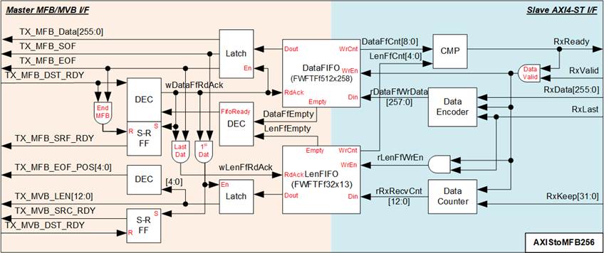
Figure 18 AXIStoMFB256 Block Diagram
Write FIFO (Slave AXI4-ST I/F)
Because the AXI4-ST I/F does not explicitly provide an SOF signal, the Data Encoder logic within the AXIStoMFB256 module generates the SOF flag internally. The SOF flag is asserted when the first data beat of a packet is received. This flag, together with the 256-bit data (RxData) and the RxLast signal, is packed into a 258-bit word and written into the DataFIFO.
When valid data is received from the AXI4-ST I/F (indicated by RxReady=1b and RxValid=1b), the write enable of the DataFIFO is asserted to store the incoming 258-bit data. At the same time, a Data Counter is incremented to track the total packet size in bytes. Since the final data beat of a packet may not fully utilize all 256 bits, the Data Counter uses the RxKeep signal to determine the number of valid bytes in the last data beat. When the end of the packet is detected, the computed packet length is written into the LenFIFO.
Read FIFO (Master MFB/MVB I/F)
The Read FIFO operation begins when both the DataFIFO and LenFIFO contain valid data, ensuring that at least one complete packet has been fully buffered. Packet data is then transmitted from the DataFIFO to the MFB interface in a continuous manner. During packet transmission, the TX_MFB_SRC_RDY signal is asserted at the first data beat and remains asserted until the last data beat of the packet is transmitted, after which it is de-asserted. Each 258-bit entry read from the DataFIFO is mapped to the MFB interface as follows: TX_MFB_DATA (bits[255:0]), TX_MFB_SOF (bit[256]), and TX_MFB_EOF (bit[257]).
When the first data beat of a packet is transmitted, the corresponding packet length is read from the LenFIFO and forwarded on the MVB interface via TX_MVB_LEN, with TX_MVB_SRC_RDY asserted. The lower five bits of the packet length are used to derive the value of TX_MFB_EOF_POS, which indicates the byte position of the final valid byte within the last MFB data word.
The LenFIFO entry is flushed when the last data beat of the packet is read from the DataFIFO, ensuring that both FIFOs are cleared of the data and corresponding metadata for the fully transmitted packet. After completing transmission of the current packet, the Read FIFO logic prepares for the next packet.
2.3.8 MFBtoAXIS256
The MFBtoAXIS256 module transfers packet data from the Calypte DMA through the MFB and MVB interfaces and forwards it to the DataMover via an AXI4-Stream interface. To ensure uninterrupted packet transfer, the module incorporates internal FIFOs to buffer incoming data when the DataMover is temporarily unable to accept new packets.
The internal logic of the MFBtoAXIS256 module is divided into four functional blocks: MFB/MVB I/F Flow Control, MFB Data Transfer, FIFO Write Controller, and FIFO Read Controller. The operation of each block is described in the following sections.
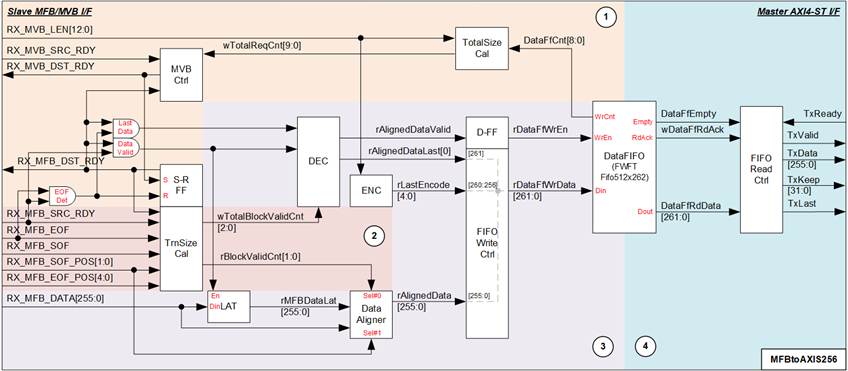
Figure 19 MFBtoAXIS256 Block Diagram
Block (1): MFB/MVB I/F Flow Control
The flow control of the MFB/MVB interfaces generates two output signals: RX_MVB_DST_RDY and RX_MFB_DST_RDY. For simplicity, the design allows only one request to be accepted on the MVB interface, followed by the reception of one packet payload on the MFB interface.
The sequence for asserting RX_MVB_DST_RDY and RX_MFB_DST_RDY is as follows:
1) The controller waits for a new request on the MVB interface (RX_MVB_SRC_RDY=1b). The request is accepted by asserting RX_MVB_DST_RDY to 1b for one clock cycle when the following conditions are satisfied:
· Both RX_MVB_DST_RDY and RX_MFB_DST_RDY are de-asserted (0b), indicating that the module is in the idle state.
· The Data FIFO has sufficient free space to store the entire packet, as determined by the wTotalReqCnt signal. The wTotalReqCnt value is calculated based on RX_MVB_LEN (which indicates the packet length of the current request) and DataFfCnt (which indicates the current data count in the FIFO).
2) After the request is accepted, RX_MFB_DST_RDY is asserted to 1b, allowing payload data transfer on the MFB interface. This signal remains asserted until the end of the packet is received, which is indicated by RX_MFB_DST_RDY=1b, RX_MFB_SRC_RDY=1b, and RX_MFB_EOP=1b simultaneously. Once packet reception is complete, the controller returns to the idle state and waits for the next request.
3) The module enters the idle state by de-asserting both RX_MVB_DST_RDY and RX_MFB_DST_RDY to 0b.
Block (2): MFB Data Transfer
Once a request on the MVB interface has been accepted, packet transfer on the MFB interface is initiated. According to the MFB interface specification, the following constraints apply to the SOF and EOF signals:
· In each clock cycle, RX_MFB_SOF can be asserted to 1b at most once. Similarly, RX_MFB_EOF can be asserted to 1b at most once.
· RX_MFB_SOF_POS indicates the position of the first packet data in 64-bit units. For a 256-bit data bus, this value ranges from 0 to 3.
· RX_MFB_EOF_POS indicates the position of the last packet data in 8-bit units. For a 256-bit data bus, this value ranges from 0 to 31.
· If both RX_MFB_SOF and RX_MFB_EOF are asserted to 1b in the same clock cycle, the cycle may contain either one or two packets, depending on the values of RX_MFB_SOF_POS and RX_MFB_EOF_POS. If the SOF position is lower than the EOF position, only one packet is transferred in that clock cycle. Otherwise, two packets are transferred, consisting of the end of one packet followed by the beginning of the next packet.
Based on these rules, data from the MFB interface is written to the DataFIFO when a full 256-bit data word is accumulated or when an EOF flag is detected. To support this behavior, the TrnSizeCal sub-block tracks both the currently received data and any unwritten residual data by generating the wTotalBlockValidCnt signal.
The wTotalBlockValidCnt signal is defined in 64-bit units and is implemented as a 3-bit value ranging from 0 to 7. This range covers the maximum possible data combination in a single clock cycle, where up to three 64-bit units may remain unwritten from the previous cycle and up to four new 64-bit units may be received. In addition, rBlockValidCnt is generated to indicate the amount of data that remains unwritten to the FIFO in the current clock cycle.
Block (3): FIFO Write Controller
According to the MFB interface specification, the first data byte of a packet is not required to be aligned to the lowest byte position of RX_MFB_DATA. However, this behavior is not compatible with the AXI4-Stream interface of the DataMover, which requires the first data byte of a packet to be aligned to the lowest byte position of TXDATA. Therefore, the received MFB data must be realigned before being written into the DataFIFO.
The DataAligner sub-block performs this alignment by packing the newly received MFB data (RX_MFB_DATA) with any unwritten data stored in rMFBDataLat. During this process, the first valid byte of the packet is realigned to the lowest byte position. In most cases, the alignment operation is controlled by rBlockValidCnt, which indicates the amount of residual data. In the special case where an entire packet is received within a single clock cycle, the RX_MFB_SOF_POS signal is used instead. The output of the DataAligner, rAlignedData, is a 256-bit data word written into the DataFIFO.
The DataFIFO stores a total of 262 bits per entry, consisting of 256-bit aligned payload data, a 5-bit encoded field indicating the number of valid bytes in the last data beat (decoded from RX_MVB_LEN), and a last flag indicating the end of a packet.
The wTotalBlockValidCnt signal is decoded to generate two control signals:
· rAlignedDataValid, which is asserted to 1b when a full 256-bit data word is accumulated or when the last packet data is received, and
· rAlignedDataLast, which indicates that the aligned data written to the DataFIFO in the current clock cycle corresponds to the final data of a packet.
Block (4): FIFO Read Controller
The FIFO Read Controller operates when valid data is available in the DataFIFO. The controller reads entries from the DataFIFO and decodes the encoded length field in DataFfRdData to determine the number of valid bytes in the current data beat.
After decoding the length information, the controller forwards the payload data to the DataMover by asserting TxValid to 1b. When the DataMover acknowledges the transfer by asserting TxReady to 1b, the controller proceeds to read the next data entry from the DataFIFO and forwards it in the same manner. This process continues until the DataFIFO becomes empty. At that point, the controller de-asserts TxValid to 0b and waits for new data to become available.
2.3.9 MI2LAxi
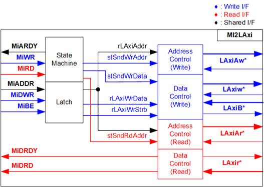
Figure 20 MI2LAxi Interface
The MI2LAxi module receives register read and write commands from the MI Splitter and forwards them to the User Logic and Ethernet Subsystem through an AXI4-Lite bus interface. This module employs a Finite State Machine (FSM) to control the command flow, ensuring that only one transaction is processed at a time.
When a write command is received, the FSM transitions through the following Write states:
· stSndWrAddr: Issues the write request along with the target address via the LAxiAw* signal group.
· stSndWrData: Transfers write data via the LAxiw* signal group.
· stWtWrResp: Waits for the write response from the AXI4-Lite slave module via the LAxiB* signal group.
When a read command is received, the FSM transitions to the following Read states:
· stSndRdAddr: Initiates a read request with the target address via the LAxiAr* signal group.
· stWtRdData: Waits for read data returned by the AXI4-Lite slave via the LAxir* signal group.
The read data received from the AXI4-Lite interface is forwarded back to the MI Splitter. During an active transaction, the MI2LAxi module does not accept new commands until the current operation is fully completed.
For more information on designing custom logic for the AXI4-Lite bus, refer to the following documentation.
3 Host Software
In the AAT-Calypte DMA demo, the Host software is divided into two main components: the NFB Framework and the AAT-Calypte application, as illustrated in Figure 21.
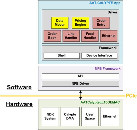
Figure 21 Host Software Structure on AAT-Calypte DMA Demo
To enable efficient communication between hardware and software, the NFB Framework is used as the software access layer. When combined with the NDK system, it allows the FPGA card to be accessed directly from user-space software, bypassing traditional operating system (OS) kernel data paths. In this reference design, the framework is tailored for use with the NDK system and the Calypte DMA implemented on the FPGA, and is therefore responsible for fulfilling Direct Memory Access (DMA) requirements. It also provides an application programming interface (API) that exposes predefined functions for DMA transactions and hardware register access.
Built on top of this framework, the AAT-Calypte application manages demo initialization, configuration, hardware register access, and system monitoring. The application is structured into two key sub-blocks.
The first sub-block is the Framework, which comprises a set of shared software functions commonly used across software components. These include functions for user interaction via the terminal (Shell) and functions that interface with the NFB Framework to perform DMA operations and access hardware registers (Device Interface).
The second sub-block is the Driver, which serves as the control interface for individual hardware submodules implemented on the FPGA. For hardware configuration and control, the Driver performs register read and write operations. For data transfer, it requests DMA transactions to move data between hardware and software. To manage multiple hardware blocks, the Driver is further divided into sub-drivers, each dedicated to a specific hardware module. For example, the Ethernet driver controls the Ethernet Subsystem, while the Feed Handler driver manages the Feed Handler within the User Module.
Similar to the hardware implementation, the Host software is pre-built to support both "Price Engine on Card" and "Price Engine Software" modes. In this design, the Data Mover and Pricing Engine drivers are always visible to the software. However, if a driver attempts an operation that is incompatible with the currently configured mode ("Price Engine on Card" or "Price Engine Software"), the software either reports a failure status to the user or returns an empty response from the hardware. These conditions do not affect the overall operation of the AAT-Calypte DMA demo.
Detailed information of the Host
software is described in the following sections.
3.1 NFB Framework
The NFB Framework provides a complete software stack for NDK-based FPGA devices. It consists of kernel drivers, the “libnfb” user-space library, and associated configuration tools. The “libnfb” library exposes a standardized API that abstracts hardware-specific details, enabling applications to access DMA controllers, manage network data flows, and configure FPGA components through an intuitive device tree interface.
This reference design follows the recommended workflow for initialization, register access, and DMA data transfer between the FPGA and the Host software, as described in the libnfb example documentation:
https://cesnet.github.io/ndk-sw/libnfb-example.html
Additional details on individual libnfb APIs are available at:
https://cesnet.github.io/ndk-sw/libnfb-api-base.html
The initialization sequence used in this reference design is illustrated in the flowchart shown in Figure 22.
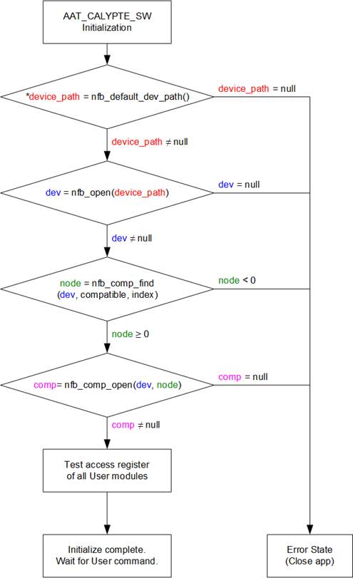
Figure 22 Initialization Flow of Host Software
1) FPGA Device Discovery: After the application is launched, the Host software calls the “nfb_default_dev_path” API to locate the target FPGA device connected to the host system. This API supports configurations in which a single FPGA card is present and returns the device path of the detected FPGA. The returned device path is then used as input for subsequent NFB API calls.
2) Device Opening: Using the retrieved device path, the software opens the FPGA device by calling the “nfb_open” API. The resulting device handle (dev) is used for all subsequent component discovery and access operations.
3) Target Component Identification: Before accessing the registers of any hardware module, the Host software identifies the corresponding component using the “nfb_comp_find” API. This API requires the device handle obtained from “nfb_open”, along with a compatible string and index that uniquely identify the target component. The compatible strings and index values used in this reference design are listed in Table 3.
Table 3 "nfb_comp_find" API Compatible String and Index
|
component |
compatible |
index |
|
MI_Test_Space |
“cesnet,ofm,mi_test_space” |
0 |
|
Calypte DMA-IP |
“netcope,dma_ctrl_ndp_rx” or “netcope,dma_ctrl_ndp_tx” |
0-15 |
|
SDM_Ctrl |
“netcope, intel_sdm_controller” |
0 |
|
User Module |
“cesnet,minimal,app_core” |
0 |
4) Component Opening: Once the target component is identified, the Host software opens it using the “nfb_comp_open” API. The returned component handle enables direct access to the registers of the selected hardware module.
When switching access between different hardware modules, the currently opened component must first be closed by calling “nfb_comp_close”, followed by reopening the new target component using “nfb_comp_find” and “nfb_comp_open.”
In this reference design, only the User Module registers are accessed. Therefore, “nfb_comp_find” and “nfb_comp_open” are invoked only once during application initialization, and “nfb_comp_close” is called when the application exits.
5) Register Access: After the target component has been successfully opened, the Host software performs hardware register accessing suing the “nfb_comp_write” and “nfb_comp_read” APIs for write and read operations, respectively.
6) DMA Data Reception (Pricing Engine on Host Software Mode): When operating in Pricing Engine on Host Software mode, the Host software continuously polls the “ndp_rx_burst_get” API in a dedicated thread to receive data from the FPGA with minimal latency. Using a separate polling thread ensures that incoming data is processed immediately, thereby minimizing end-to-end latency.
7) DMA Data Transmission: Once the Pricing Engine generates a trading decision and creates an order, the Host software calls “ndp_tx_burst_get” to transmit the order to the FPGA. The FPGA then constructs the corresponding order packet and forwards it to the target destination.
3.2 AAT-Calypte Framework
The AAT-Calypte Framework gathers common software functions, providing a structured foundation for efficient and reusable operations across the AAT-Calypte DMA system. It is divided into two main sections: Shell, for command-line interactions, and Device Interface, for hardware operations.
3.2.1 Shell
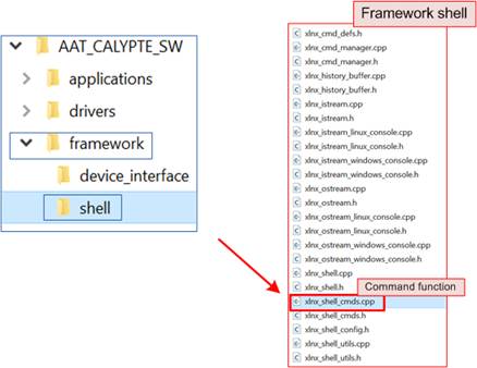
Figure 23 AAT-Calypte Shell
The Shell is a collection of source code linked to the AAT-Calypte shell commands, offering 10 executable functions within the AAT-Calypte console. These functions enable users to interact directly with the hardware, allowing for control, configuration, and monitoring operations. The functions are implemented in the file “xlnx_shell_cmds.cpp”, as illustrated in Figure 23.
Table 4 lists the available shell commands and their corresponding functions.
Table 4 Shell Commands in AAT-Calypte Framework
|
Command |
Argument |
Description |
|
help |
<object> |
Print a list of objects and commands |
|
exit |
none |
Exit the shell instance |
|
quit |
none |
Exit shell instance |
|
history |
none |
List previously executed commands |
|
regrd |
<addr> |
Read a single 32-bit register |
|
regwr |
<addr> <value> |
Write to a single 32-bit register |
|
regwrm |
<addr> <value> <mask> |
Write to a register with a mask |
|
reghexdump |
<addr> |
Perform a hex dump of registers starting at <addr> |
|
run |
<filepath> |
Execute a script containing shell commands |
|
touch |
<filepath> |
Change file timestamps |
3.2.2 Device Interface
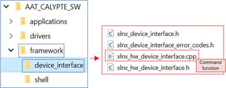
Figure 24 AAT-Calypte Device Interface
The Device Interface facilitates hardware communication by providing functions to write and read registers, which are extensively utilized throughout the AAT-Calypte application. It defines seven primary functions for hardware interaction, declared in the file “xlnx_hw_device_interface.cpp”. The directory structure for this file is shown in Figure 24.
Below is the list of functions provided by the Device Interface.
|
HWDeviceInterface::HWDeviceInterface() |
|
|
Parameters |
None |
|
Return value |
None |
|
Description |
Constructor that initializes the class instance and sets default values. |
|
HWDeviceInterface::~HWDeviceInterface() |
|
|
Parameters |
None |
|
Return value |
None |
|
Description |
Destructor that cleans up dynamically allocated resources. |
|
uint32_t HWDeviceInterface::ReadReg32(uint64_t address, uint32_t* value) |
|
|
Parameters |
address: Address of the register value: Pointer to store the read value |
|
Return value |
XLNX_OK (defined as 0x00000000) on success, or an error code |
|
Description |
Reads a 32-bit register value from the specified hardware address. |
|
uint32_t HWDeviceInterface::WriteReg32(uint64_t address, uint32_t value) |
|
|
Parameters |
address: Address of the register value: Value to be written |
|
Return value |
XLNX_OK (defined as 0x00000000) on success, or an error code |
|
Description |
Writes a 32-bit value to the specified hardware address. |
|
uint32_t HWDeviceInterface::WriteRegWithMask32(uint64_t address, uint32_t value, uint32_t mask) |
|
|
Parameters |
address: Address of the register value: Value to be written mask: Bitmask specifying the bits to modify |
|
Return value |
XLNX_OK (defined as 0x00000000) on success, or an error code |
|
Description |
Writes a 32-bit value to a register, applying a bitmask to modify only specific bits. |
|
uint32_t HWDeviceInterface::BlockReadReg32(uint64_t address, uint32_t* buffer, uint32_t numWords) |
|
|
Parameters |
address: Starting address buffer: Pointer to buffer for storing read values numWords: Number of 32-bit words to read |
|
Return value |
XLNX_OK (defined as 0x00000000) on success, or an error code |
|
Description |
Reads multiple 32-bit values from consecutive hardware registers into a buffer. |
|
uint32_t HWDeviceInterface::BlockWriteReg32(uint64_t address, uint32_t* buffer, uint32_t numWords) |
|
|
Parameters |
address: Starting address buffer: Pointer to buffer containing values to write numWords: Number of 32-bit words to write |
|
Return value |
XLNX_OK (defined as 0x00000000) on success, or an error code |
|
Description |
Writes multiple 32-bit values from a buffer to consecutive hardware registers. |
3.3 AAT-Calypte Driver
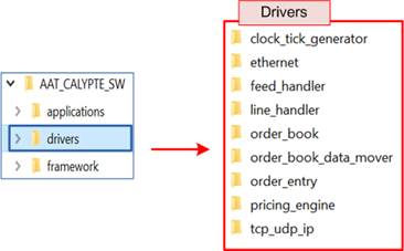
Figure 25 AAT-Calypte Driver
The AAT-Calypte Driver is a software layer designed to control and monitor hardware components of the AAT-Calypte DMA system. It performs write and read operations to the target hardware registers, enabling configuration, status retrieval, and operational control.
The driver is organized into sub-drivers, each dedicated to managing a specific hardware block, such as Clock Tick Generator, DataMover, or OrderEntry modules. Each sub-driver comprises a driver implementation and a set of shell command handlers that are registered with the common command shell framework. The driver implementation provides low-level functions to interact with hardware registers, while the shell command handlers expose a high-level user interface for configuration and debugging.
Detailed descriptions of each sub-driver and its associated command handlers are provided in the following sections.
3.3.1 ClockTick Generator
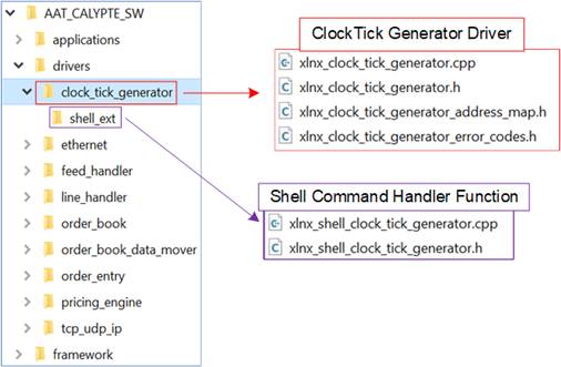
Figure 26 ClockTick Generator Driver
The ClockTick Generator driver provides control and monitoring of programmable tick events for the AAT-Calypte DMA system. It supports configuring tick intervals, enabling or disabling specific tick streams, resetting internal counters without triggering output, and retrieving block status.
The driver interacts with hardware registers implemented in “xlnx_clock_tick_generator.cpp”, while user interaction is provided via shell command handlers defined in “xlnx_shell_clock_tick_generator.cpp”.
The commands available in the shell command handlers for managing the ClockTick Generator are listed in Table 5.
Table 5 ClockTick Generator Shell Command Handlers
|
Command |
Argument |
Description |
|
setenable |
<index> <bool> |
Enable or disable a specific tick stream |
|
setinterval |
<index> <usecs> |
Set the tick event interval in microseconds |
|
getstatus |
None |
Retrieve the block status |
3.3.2 Ethernet
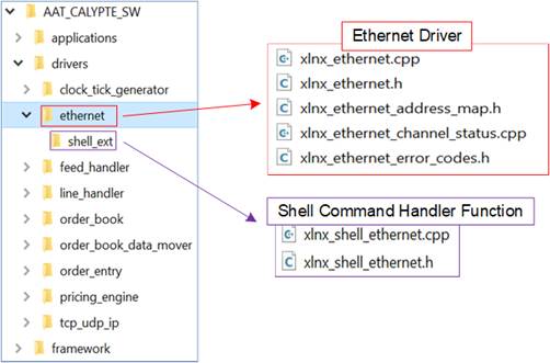
Figure 27 Ethernet Driver
The Ethernet driver manages the Ethernet hardware by performing register read and write operations. It enables monitoring, configuration, and control of Ethernet functionality, such as retrieving status, printing diagnostics, and resetting latches for each channel. The driver interacts with the hardware via registers defined in “xlnx_ethernet_address_map.h”, while error codes are specified in “xlnx_ethernet_error_codes.h”.
The core driver is implemented in “xlnx_ethernet.cpp” and “xlnx_ethernet_channel_status.cpp”, and user interaction is facilitated through shell command handlers defined in “xlnx_shell_ethernet.cpp”.
The commands available in the shell command handlers for managing the Ethernet are listed in Table 6.
Table 6 Ethernet Shell Command Handlers
|
Command |
Argument |
Description |
|
getstatus |
None |
Retrieve the status of Ethernet channels |
|
clearlatches |
<channel> |
Clear/reset status latches for the specified channel |
|
gethwdebuginfo |
<channel> |
Retrieve detailed debugging information for a specific channel |
3.3.3 Feed Handler
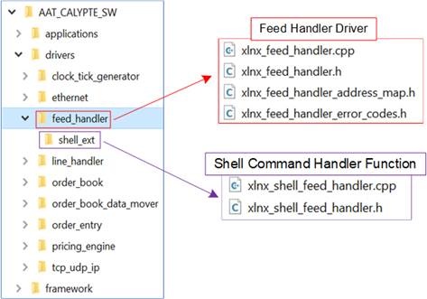
Figure 28 Feed Handler Driver
The Feed Handler driver manages securities and trading updates for CME trading using register write and read operations. It supports adding, deleting, and refreshing securities; controls start, stop, or reset operations of the corresponding hardware block; and provides monitoring of hardware status and statistics. The core functionality is implemented in “xlnx_feed_handler.cpp”, while user interaction is facilitated through shell command handlers defined in “xlnx_shell_feed_handler.cpp”.
The commands available in the shell command handlers for managing the Feed Handler are listed in Table 7.
Table 7 Feed handler Shell Command Handlers
|
Command |
Argument |
Description |
|
add |
<securityID> |
Add a security at the first available index |
|
addat |
<securityID> <index> |
Add a security at a specific index |
|
delete |
<securityID> |
Delete a security |
|
deleteall |
None |
Delete all securities |
|
start |
None |
Start block processing |
|
stop |
None |
Stop block processing |
|
getstatus |
None |
Get block status |
|
list |
None |
Print a list of securities |
|
refresh |
None |
Refresh the internal security ID cache |
|
resetstats |
None |
Reset statistics counters |
|
readdata |
None |
Read the last captured data |
3.3.4 Line Handler
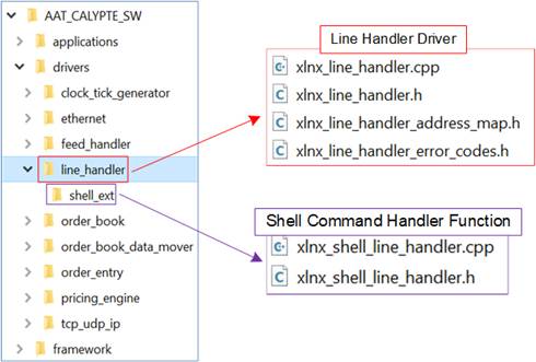
Figure 29 Line Handler Driver
The Line Handler driver manages UDP multicast feeds by interacting with hardware control registers. It supports advanced configuration and monitoring capabilities, including multicast filter management, reliability mode selection, sequence timing control, and debug features such as traffic echoing.
The core driver implementation is provided in “xlinx_line_handler.cpp”, while the shell command handlers for user interaction are defined in “xlnx_shell_line_handler.cpp”.
The commands available in the shell command handlers for managing the Line Handler are listed in Table 8.
Table 8 Line Handler Shell Command Handlers
|
Command |
Argument |
Description |
|
getstatus |
None |
Retrieve the Line Handler block status |
|
add |
<inputport> <ipaddr> <port> <splitID> |
Add a multicast filter for a port |
|
delete |
<inputport> <ipaddr> <port> <splitID> |
Delete a multicast filter from a port |
|
deleteall |
<inputport> |
Clear all multicast filters for a port |
|
setechoenabled |
<inputport> <bool> |
Enable or disable debug traffic echo |
|
setechodest |
<inputport> <ipaddr> <port> |
Set UDP destination for debug echo |
|
setsequencetimer |
<microseconds> |
Set the sequence reset timer |
|
resetsequence |
None |
Reset the sequence number |
|
sethighreliability |
<bool> |
Enable or disable high reliability mode |
|
setspooltimerlimit |
<microseconds> |
Set spool timeout limit before aborting |
|
setspoolpacketlimit |
<numpackets> |
Set spool packet limit before aborting |
|
setdequeuethrottle |
<throttlerate> |
Set the dequeue throttle rate (in clock cycles) |
3.3.5 OrderBook
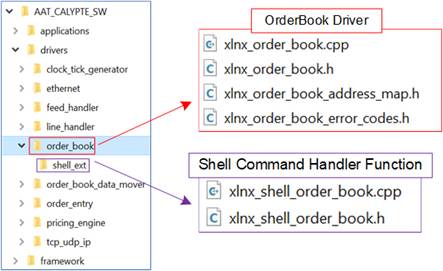
Figure 30 OrderBook Driver
The OrderBook driver manages control and monitoring of the OrderBook hardware functionality. It enables starting and stopping the processing block, configuring the capture index for ticker symbols, and enabling or disabling output to the DataMover submodule. The driver also facilitates status monitoring, reading aggregated order data, and resetting statistical counters.
The driver implementation is provided in “xlnx_order_book.cpp”, while the shell command handlers for user interaction are defined in “xlnx_shell_order_book.cpp”.
The commands available in the shell command handlers for managing the OrderBook are listed in Table 9.
Table 9 OrderBook Shell Command Handlers
|
Command |
Argument |
Description |
|
getstatus |
None |
Get the status of the OrderBook block |
|
readdata |
None |
Read aggregated order book data |
|
resetstats |
None |
Reset statistical counters |
|
setcaptureindex |
<symbolindex> |
Set the symbol index for data filtering |
|
setdmoutput |
<bool> |
Enable or disable output to the DataMover submodule |
|
start |
None |
Start the OrderBook processing block |
|
stop |
None |
Stop the OrderBook processing block |
3.3.6 DataMover
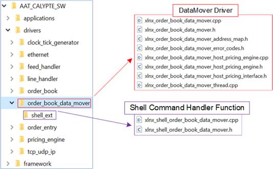
Figure 31 DataMover Driver
The DataMover driver facilitates data transfer between the OrderBook hardware and the Pricing Engine software, using NFB APIs to communicate with the Calypte DMA. It provides comprehensive control over DMA operations, including configuration of DMA chunk sizes, management of processing threads, and resetting of DMA statistics. It also supports debugging with verbose output and performs round-trip latency measurements to evaluate communication efficiency.
The core driver implementation in “xlnx_order_book_data_mover.cpp”, while the shell command handlers are defined in “xlnx_shell_order_book_data_mover.cpp”.
The DataMover operates exclusively in “Pricing Engine Software” mode, where the Pricing Engine software processes OrderBook data received from hardware and sends corresponding trade operations back to the DataMover submodule for execution. The DMA operations are handled by the “Threadfunc” function, implemented as “OrderBookDataMover::ThreadFunc” declared in “xlnx_order_book_data_mover_thread.cpp”.
The sequence of operations performed by “ThreadFunc” is outlined below.
Initialization
1) Define NFB Framework parameters, including the receive and transmit queues (ndp_queue *rxq and *txq), receive packet buffers (rxPkt), and transmit packet buffer (txPkt).
2) Open the receive and transmit queues using “ndp_open_rx_queue” and “ndp_open_tx_queue”.
3) Start the opened queues using “ndp_queue_start”.
Active Processing
1) Enter the main processing loop and continuously poll for received packets using “ndp_rx_burst_get”.
2) For each received packet, unpack the data using “UnpackResponse” and pass the extracted response data to “ProcessPricingData”, which evaluates whether a valid trade operation should be generated.
3) If the Pricing Engine software determines that the operation is valid (bOperationValid = 1), pack the operation using “PackOperation” and transmit it to the hardware via “ndp_tx_burst_get”. The transmitted packet count is updated in “m_threadStats.numTxPackets”.
If the operation is not valid, the unexecuted operation counter (“m_threadStats.numNoExecutions”) is incremented.
4) Release processed receive packets back to the RX queue using “ndp_rx_burst_put”.
5) If “m_bYield” is enabled, yield the thread using “std::this_thread::yield” to allow other processes to execute. Otherwise, the thread continues running until it is stopped by the system or completes its task.
Clean up
1) Close the transmit queue using “ndp_close_tx_queue”.
2) Close the receive queue using “ndp_close_rx_queue”.
The Host Pricing Engine driver can be customized in the “HostPricingEngine::PricingProcess” function, implemented in “xlnx_order_book_data_mover_host_pricing_engine.cpp” file, allowing the pricing strategy to be adapted to specific application requirements. The file structure is illustrated in Figure 31.
The shell command handlers associate with the Data Mover are listed in Table 10.
Table 10 DataMover Shell Command Handlers
|
Command |
Argument |
Description |
|
getstatus |
None |
Retrieve the DataMover block status |
|
start |
None |
Start DataMover operations |
|
timing |
None |
Perform round-trip latency measurement |
|
verboseon |
None |
Enable detailed debug logging |
|
verboseoff |
None |
Disable detailed debug logging |
|
threadstart |
None |
Start the Pricing Engine thread |
|
threadstop |
None |
Stop the Pricing Engine thread |
|
threadyield |
<bool> |
Enable or disable thread yielding |
|
resetdmastats |
None |
Reset DMA statistics counters |
|
sethwemupolldelay |
<seconds> |
Set polling delay for hardware emulation mode |
3.3.7 OrderEntry
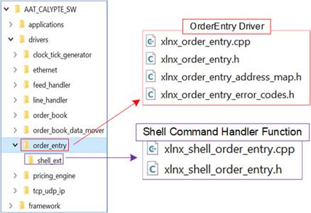
Figure 32 OrderEntry Driver
The OrderEntry driver manages the creation and transmission of trading orders by interacting with hardware control registers. It facilitates configuring connections to remote systems, generating partial checksums, monitoring hardware status, and resetting statistical counters. The driver also provides the ability to read the most recently transmitted message and to establish or re-establish TCP connections.
The driver implementation is provided in “xlnx_order_entry.cpp”, while the shell command handlers for user interaction are defined in “xlnx_shell_order_entry.cpp”.
The commands available in the shell command handlers for managing the OrderEntry are listed in Table 11.
Table 11 OrderEntry Shell Command Handlers
|
Command |
Argument |
Description |
|
getstatus |
None |
Retrieve block status |
|
readmsg |
None |
Read the last emitted message |
|
resetstats |
None |
Reset statistics counters |
|
connect |
<ipaddr> <port> |
Establish connection to a remote system |
|
disconnect |
None |
Close the connection to the remote system |
|
reconnect |
None |
Close and re-open an existing connection |
|
setcsumgen |
<bool> |
Enable or disable partial checksum generation |
3.3.8 Pricing Engine
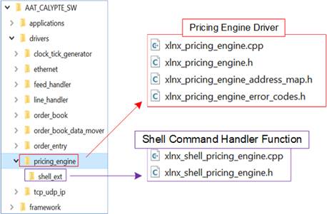
Figure 33 Pricing Engine Driver
The Pricing Engine driver manages and monitors trading strategies and rules for specified symbols by interacting with hardware control registers. It supports configuring global trading modes and strategies, monitoring block status, reading trading data, and resetting statistical counters. These capabilities enable dynamic control of trading logic and parameters based on OrderBook updates.
The driver implementation is provided in “xlnx_pricing_engine.cpp”, while the shell command handlers for user interaction are defined in “xlnx_shell_pricing_engine.cpp”.
The commands available in the shell command handlers for managing the Pricing Engine are listed in Table 12.
Table 12 Pricing Engine Shell Command Handlers
|
Command |
Argument |
Description |
|
setglobalmode |
<bool> |
Enable or disable global pricing strategy |
|
setglobalstrategy |
<none|peg|limit> |
Set the global trading strategy applied to all symbols |
|
getstatus |
None |
Retrieve the block status |
|
readdata |
None |
Read trading data for the last operation |
|
resetstats |
None |
Reset statistical counters |
3.3.9 TCP/UDP IP
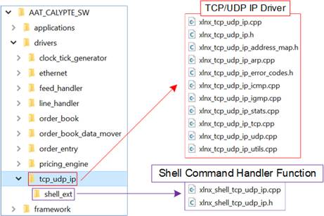
Figure 34 TCP/UDP IP Driver
The TCP/UDP IP driver provides comprehensive control and monitoring of TCP and UDP networking functionalities by interacting with hardware registers. In addition to basic network configuration, it supports advanced features such as IGMP (Internet Group Management Protocol), ARP (Address Resolution Protocol), ICMP (Internet Control Message Protocol), and multicast operations. The driver also enables data path configuration, and statistics monitoring.
The driver implementation is divided into multiple protocol-specific modules, including ARP, ICMP, IGMP, and UDP, with core functionality implemented in “xlnx_tcp_udp_ip.cpp”. User interaction is provided through shell command handlers defined in “xlnx_shell_tcp_udp_ip.cpp”., where commands are grouped into four categories: Network Parameter Configuration, UDP Configuration, ARP Configuration and Block Management.
Network Parameter Configuration
This category provides commands to configure basic network parameters such as the MAC address, IPv4 address, subnet mask, and gateway address. The available commands are summarized in Table 13.
Table 13 Network Configuration Shell Command Handlers
|
Command |
Argument |
Description |
|
setmacaddr |
<macaddr> |
Set the MAC address |
|
setipaddr |
<ipaddr> |
Set the IPv4 address |
|
setsubnetmask |
<ipmask> |
Set the subnet mask |
|
setgateway |
<ipaddr> |
Set the gateway IPv4 address |
UDP Configuration
The UDP configuration commands allow management of IGMP settings, multicast address, ICMP behavior, and UDP listening ports. The available commands are listed in Table 14.
Table 14 UDP Configuration Shell Command Handlers
|
Command |
Argument |
Description |
|
setigmp |
<bool> |
Enable or disable IGMP |
|
setigmpver |
<ver> |
Set the IGMP version (2 or 3) |
|
igmpprint |
<ipaddr> |
Print the contents of the IGMP table |
|
addmcast |
<ipaddr> |
Add a multicast IP address |
|
deletemcast |
<ipaddr> |
Delete a multicast IP address |
|
seticmp |
<bool> |
Enable or disable ICMP |
|
addport |
<portnum> |
Add a UDP listening port |
|
deleteport |
<portnum> |
Delete a UDP listening port |
|
deleteallports |
None |
Delete all UDP listening ports |
ARP Configuration
This category manages the ARP table, allowing users to print, add, delete, or clear ARP entries. The available commands are summarized in Table 15.
Table 15 ARP Configuration Shell Command Handlers
|
Command |
Argument |
Description |
|
arpprint |
None |
Print the contents of the ARP table |
|
arpadd |
<ipaddr> <macaddr> |
Add an ARP entry |
|
arpdelete |
<index> |
Delete an ARP entry at the specified index |
|
arpdeleteall |
None |
Delete all ARP entries |
Block Management
Block management commands provide control over statistics monitoring and configuration access. These commands are summarized in Table 16.
Table 16 Block Management Shell Command Handlers
|
Command |
Argument |
Description |
|
printstats |
None |
Print protocol-specific statistics counters |
|
getstatus |
None |
Retrieve the block status information |
|
setconfigallowed |
<bool> |
Enable or disable configuration writes |
3.4 AAT-Calypte Application
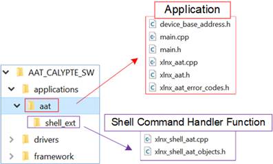
Figure 35 AAT-Calypte Application
The AAT-Calypte Application provides a unified software platform for controlling and monitoring FPGA-based hardware components through a command-driven interface. It integrates multiple hardware drivers to offer seamless interaction between the Host software and the AAT-Calypte DMA system for trading applications.
The application is divided into two key components. The first is the “Shell Command Handler”, which provides a command-line interface for executing user-defined operations. The second is the “Application”, which manages system initialization, hardware communication, and coordination between software and hardware components.
3.4.1 Shell Command Handler
The Shell Command Handler enables user interaction with the AAT-Calypte DMA system through predefined commands. These commands allow users to retrieve the status of the hardware objects, reinitialize system components, and start the DataMover for transferring OrderBook output to the Host Pricing Engine.
The shell command handlers are implemented in “xlnx_shell_aat.cpp”, and the available commands are listed in Table 17.
Table 17 AAT-Calypte Application Shell Command Handler
|
Command |
Argument |
Description |
|
getstatus |
None |
Retrieve the status of individual hardware objects |
|
reinit |
None |
Reinitialize all AAT-Calypte objects |
|
startdatamover |
None |
Start the DataMover submodule and enable OrderBook output |
3.4.2 Application
The AAT-Calypte Application is responsible for initializing and managing hardware components and for binding command tables to the shell command handler for user interaction. Its operation is divided into two phases: Initialization and Idle.
Initialization
During the initialization phase, the application configures both hardware and software resources and prepares the system to accept user commands.
1) The application initializes the NFB Framework and opens the User Module and Ethernet Subsystem components to enable register access register for hardware control and monitoring.
2) Input and output streams are configured for console interaction, with settings adapted for compatibility with Linux or Windows environments.
3) The main application object (“g_aat”) is initialized and associated with the hardware device interface to establish communication between the application and the hardware. During this step, the base address of each hardware block is assigned to its corresponding software driver.
4) Command tables for the various hardware components are registered with the shell command handler using “AddObjectCommandTable”, ensuring that all hardware objects and their associated commands are accessible through the shell command handlers.
Idle
After initialization, the application enters the Idle state, where the shell command handler is ready to accept user commands. The shell command handler supports two modes of operation: One-Shot Mode and Interactive Mode.
· One-Shot Mode: In this mode, a single command is executed directly from the command line. This mode is suitable for automated scripts or scenarios where a specific operation needs to be performed without entering an interactive session. For example:
>> ./AAT_CALYPTE aat getstatus
· Interactive Mode: This mode opens an interactive console session, allowing users to enter multiple commands continuously. It is particularly useful for debugging, testing, or real-time system management. The session remains active until the user exits explicitly. For example:
>> ./AAT_CALYPTE
In the interactive mode, commands are entered using the following format: <object> <command> [arguments].
For example: Retrieve the status of the OrderBook:
>> orderbook getstatus
Users can view the list of available commands for a specific object by typing:
>> <object> help
3.5 AAT-Calypte Script
The AAT-Calypte script consists of a sequence of commands used to configure and initialize all required hardware and software components for system operation. These scripts ensure that each component is properly set up before the demo is executed. The configuration is provided through two separate files:
· “demo_setup.cfg”: Configures the system for “Pricing Engine on Card” mode.
· “demo_setup_with_datamover.cfg”: Configures the system for “Pricing Engine on Software” mode. This configuration includes setup of the DataMover and excludes hardware Pricing Engine configuration.
3.5.1 demo_setup.cfg
The “demo_setup.cfg” file contains a sequence of commands used to initialize and configure all required system components for “Pricing Engine on Card” mode. These components include the Ethernet Subsystem, TCP/UDP IP, Line Handler, Feed Handler, Pricing Engine, OrderEntry, and ClockTick Generator.
The following sections summarize the configurations applied by this script, along with example commands and explanations.
UDP IP Configuration
The UDP IP configuration sets up network parameters and communication settings required for processing incoming UDP multicast data.
1) Assign a unique IP address to the UDP interface for network identification.
>> udpip0 setipaddr 192.168.10.200
2) Set the default gateway for packets destined for external networks.
>> udpip0 setgateway 192.168.10.100
3) Add UDP listening ports. These ports enable the device to receive incoming UDP traffic on specified port numbers, such as 14318 and 15318.
>> udpip0 addport 14318
>> udpip0 addport 15318
4) Activate the IGMP for managing multicast group memberships. This is required for multicast communication.
>> udpip0 setigmp true
5) Configure the IGMP version to 3, which supports advanced multicast features.
>> udpip0 setigmpver 3
6) Add multicast IP addresses to the IGMP table, enabling the device to join specific multicast groups for receiving group-specific data. In this example, the multicast addresses 224.0.31.9 and 224.0.32.9 are added.
>> udpip0 addmcast 224.0.31.9
>> udpip0 addmcast 224.0.32.9
TCP IP Configuration
The TCP IP configuration sets the network parameters necessary for establishing and managing TCP connections.
1) Configure the IP address for the TCP interface. This address uniquely identifies the device on the network for TCP communication.
>> tcpip setipaddr 192.168.20.200
2) Assign the gateway address, which acts as the default route for packets destined for external networks.
>> tcpip setgateway 192.168.20.100
Line Handler Configuration
The Line Handler configuration manages UDP multicast feed filtering and sequence timing for A/B market data lines.
1) Filters are configured based on input IP address, UDP port, and split ID to select the multicast feeds to be processed.
· The first command adds a filter for Line A, processing data from IP address 205.209.221.75 on port 14318 with splitID = 0.
· The second command adds a filter for Line B, processing data from IP address 205.209.212.75 on port 15318, also with splitID = 0.
>> linehandler add 0 205.209.221.75 14318 0
>> linehandler add 0 205.209.212.75 15318 0
2) Configure the sequence timer to 1000 microseconds.
>> linehandler setsequencetimer 1000
Feed Handler Configuration
The Feed Handler configuration manages the registration of Security IDs, enabling the processing of market data updates for selected securities. This setup ensures that the Feed Handler processes only the relevant data streams.
The following commands register multiple Security IDs, including standard IDs (1024, 2048, 3072, and others) and a large ID (305419896). Each registered Security ID corresponds to a specific ticker symbol or financial instrument in the market.
>> feedhandler add 1024
>> feedhandler add 2048
>> feedhandler add 3072
>> feedhandler add 4096
>> feedhandler add 5120
>> feedhandler add 6144
>> feedhandler add 7168
>> feedhandler add 8192
>> feedhandler add 9216
>> feedhandler add 10240
>> feedhandler add 305419896
Pricing Engine Configuration
The Pricing Engine configuration defines the global trading strategies and enables global pricing mode for all registered securities. These settings ensure that trading logic is applied across all securities in the system. Below are the commands and their explanations:
1) Configure the global trading strategy to “peg” using the “setglobalstrategy” command. The “peg strategy” dynamically adjusts bid and ask prices based on changes in the top-of-book (ToB) price.
>> pricingengine setglobalstrategy peg
2) Activate the global pricing mode using the “setglobalmode” command with the argument “true”. When enabled, global pricing mode applies the configured strategy to all securities.
>> pricingengine setglobalmode true
OrderEntry Configuration
The OrderEntry configuration establishes the connection to a remote system and optimizes data transmission by enabling hardware-based checksum generation. Below are the commands and their explanations:
1) Configure the OrderEntry to enable partial checksum generation using the “setcsumgen” command with the argument “true”. When enabled, the hardware offloads checksum calculations for TCP packets, reducing CPU overhead and improving transmission efficiency.
>> orderentry setcsumgen true
2) Establish a TCP connection to a remote system using the “connect” command with the specified IP address and port. In this example, the system connects to 192.168.20.100 on port 12345.
>> orderentry connect 192.168.20.100 12345
ClockTick Generator Configuration
The ClockTick Generator configuration sets precise timing intervals for each event stream and enables the streams to synchronize hardware modules in the system. Below are the commands and their explanations:
1) Configure the interval for each clock tick event stream using the “setinterval” command. In this example, stream 0 is configured with an interval of 1,000,000 microseconds (1 second).
>> clocktickgen setinterval 0 1000000
2) Activate a specific tick stream using the “setenable” command with the argument “true”. In this example, stream 0 is enabled to start generating tick events.
>> clocktickgen setenable 0 true
The ClockTick Generator supports up to 5 event streams, which can be assigned to specific hardware modules as follows: Stream 0-Feed Handler, Stream 1-OrderBook, Stream 2-Pricing Engine, Stream 3-OrderEntry, and Stream 4-Line Handler.
3.5.2 demo_setup_with_datamover.cfg
The “demo_setup_with_datamover.cfg” file is largely similar to “demo_setup.cfg”, with the following key differences:
· Enables the transmission of OrderBook data to the Pricing Engine software.
· The Pricing Engine hardware is not utilized when operating in “Pricing Engine on Software” mode.
DataMover Configuration
The DataMover configuration enables the system to transfer OrderBook data from hardware to the Pricing Engine software. Below are the commands and their explanations:
1) The “startdatamover” command initializes the DataMover submodule, allowing the OrderBook to transmit data to the Host software for pricing processing.
>> aat startdatamover
2) The “threadstart” command activates the thread responsible for running the Pricing Engine software, which processes OrderBook data received via the DataMover.
>> datamover threadstart
4 Target Software
The software running on the target system uses “tcpreplay” as a market data generator. “tcpreplay” is an open-source network traffic replay tool that allows previously captured network traffic stored in PCAP (packet capture) files to be replayed onto a live network. It is commonly used for testing and debugging network devices, applications, and security systems by simulating real-world traffic conditions.
In this design, “tcpreplay” replays the “cme_input_arb.pcap” file to simulate CME market data traffic. This enables the AAT-Calypte DMA system to receive, process, and respond to realistic market data streams under controlled test conditions.
For more information about “tcpreplay”, visit the official website:
https://tcpreplay.appneta.com/
5 Revision History
|
Revision |
Date (D-M-Y) |
Description |
|
1.00 |
3-Feb-26 |
Initial version release |